4 mm
◊ 4 mm Multianode, High Speed Response, Low Cross-talk
30 mm Square, Bialkali Photocathode, 12-stage, Head-on Type
Information furnished by HAMAMATSU is believed to be reliable. However, no responsibility is assumed for possible inaccuracies or omissions. Specifications are
subject to change without notice. No patent rights are granted to any of the circuits described herein. ©2003 Hamamatsu Photonics K.K.
Subject to local technical requirements and regulations, availability of products included in this promotional material may vary. Please consult with our sales office.
MULTIANODE
PHOTOMULTIPLIER TUBE ASSEMBLY
H8711, H8711-10
GENERAL
Parameter
Description/Value
Unit
Spectral Response
Peak Wavelength
Photocathode
Window Material
Dynode
Anode Size
Weight
Operating Ambient Temperature
Storage Temperature
nm
nm
--
mm
--
--
--
mm
g
∞C
∞C
300 to 650
420
Bialkali
18.1
◊ 18.1
Borosilicate glass
Metal channel dynode
12
4.2
◊ 4.2 (center)
Approx. 50
-30 to +50
-30 to +50
Material
Minimum Effective Area
Structure
Number of Stages
CHARACTERISTICS (at 25
∞C)
Parameter
Min.
Unit
Cathode Sensitivity
Anode Sensitivity
Gain
Anode Dark Current per Channel (after 30 min storage in darkness)
Anode Dark Current in Total (after 30 min storage in darkness)
Time Response
per Channel
Pulse Linearity per Channel (
±5 % deviation)
Cross-talk (4 mm
◊ 4 mm Aperture)
Uniformity Between Each Anode
Luminous (2856 K)
Blue Sensitivity Index (CS 5-58)
Luminous (2856 K)
Anode Pulse Rise Time
Electron Transit Time
Transit Time Spread (FWHM)
60
6.5
80 (20)
--
--
--
--
--
--
--
--
--
80
8.5
280 (70)
3.5
◊ 10
6
(0.9
◊ 10
6
)
0.8 (0.4)
12 (6)
0.83
10.9
0.3
1 (3)
1
1: 3
µA/lm
--
A/lm
--
nA
nA
ns
ns
ns
mA
%
--
--
--
--
--
--
60 (30)
--
--
--
--
--
1: 5
Typ.
Max.
NOTE: Anode characteristics are measured with the voltage distribution ratio shown below.
( ): Measured with the special voltage distribution ratio (Tapered Divider) shown below.
* The maximum average anode current is defined as 5 % of divider current when standard high voltage is applied.
MAXIMUM RATINGS (Absolute Maximum Values)
Parameter
Value
Unit
Supply Voltage
Average Anode Output Current in Total
Between Anode and Cathode
V
mA
1000
0.014*
2
1
2
2
1
1 . . . 1
1
K
Dy2
Dy5
Dy4
Dy1
Dy3
. . .
Dy9
Dy10
Dy11
Dy12
P
Supply Voltage: 800 V, K: Cathode, Dy: Dynode, P: Anode
VOLTAGE DISTRIBUTION RATIO AND SUPPLY VOLTAGE
Electrodes
H8711
H8711-10 (Tapered Divider)
1
1
1
2.4
1
2.4
2.4
1
1 . . . 1
1
1
1.2
2.4
PATENT

MULTIANODE
PHOTOMULTIPLIER TUBE ASSEMBLIES H8711, H8711-10
Figure 1: Typical Spectral Response
TPMHB0266EA
Figure 2: Typical Gain and Anode Dark Current
per Channel
TPMHB0690EA
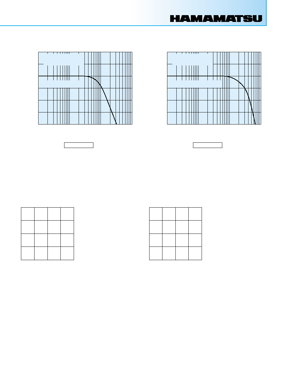
Figure 3: Typical Time Response
TPMHB0331EA
Figure 4: Typical T.T.S. Characteristic
TPMHB0314EB
10
0
10
1
10
2
10
3
10
4
TIME (0.5 ns/div.)
RELATIVE COUNTS
SUPPLY VOLTAGE= - 800 V
FWHM= 310 ps
FWTM= 631 ps
WAVELENGTH (nm)
100
200
300
400
500
600
700
800
900
0.01
0.1
1
10
100
CATHODE RADIANT SENSITIVITY (mA/W)
QUANTUM EFFICIENCY (%)
QUANTUM
EFFICIENCY
CATHODE
RADIANT
SENSITIVITY
10
1
10
2
10
3
10
4
10
5
10
6
400
600
1000
800
SUPPLY VOLTAGE (V)
GAIN
ANODE DARK CURRENT (nA)
10
7
10
8
10-
3
10-
2
10-
1
10
0
10
1
10
2
10
3
10
4
GAIN
ANODE DARK CURRENT
PER CHANNEL
H8
711
H8711
H8711
-10
H8
711
-10
TIME (2 ns/div.)
(2 mV/div.)
SUPPLY VOLTAGE
RISE TIME
FALL TIME
WIDTH
R
L
= -800 V
= 835 ps
= 2047 ps
= 1658 ps
= 50

HAMAMATSU PHOTONICS K.K., Electron Tube Center
314-5, Shimokanzo, Toyooka-village, Iwata-gun, Shizuoka-ken, 438-0193, Japan, Telephone: (81)539/62-5248, Fax: (81)539/62-2205
U.S.A.: Hamamatsu Corporation: 360 Foothill Road, P. O. Box 6910, Bridgewater. N.J. 08807-0910, U.S.A., Telephone: (1)908-231-0960, Fax: (1)908-231-1218 E-mail: usa@hamamatsu.com
Germany: Hamamatsu Photonics Deutschland GmbH: Arzbergerstr. 10, D-82211 Herrsching am Ammersee, Germany, Telephone: (49)8152-375-0, Fax: (49)8152-2658 E-mail: info@hamamatsu.de
France: Hamamatsu Photonics France S.A.R.L.: 8, Rue du Saule Trapu, Parc du Moulin de Massy, 91882 Massy Cedex, France, Telephone: (33)1 69 53 71 00, Fax: (33)1 69 53 71 10 E-mail: infos@hamamatsu.fr
United Kingdom: Hamamatsu Photonics UK Limited: 2 Howard Court, 10 Tewin Road Welwyn Garden City Hertfordshire AL7 1BW, United Kingdom, Telephone: 44-(0)1707-294888, Fax: 44(0)1707-325777 E-mail: info@hamamatsu.co.uk
North Europe: Hamamatsu Photonics Norden AB: Smidesv‰gen 12, SE-171-41 SOLNA, Sweden, Telephone: (46)8-509-031-00, Fax: (46)8-509-031-01 E-mail: info@hamamatsu.se
Italy: Hamamatsu Photonics Italia: S.R.L.: Strada della Moia, 1/E, 20020 Arese, (Milano), Italy, Telephone: (39)02-935 81 733, Fax: (39)02-935 81 741 E-mail: info@hamamatsu.it
WEB SITE http://www.hamamatsu.com
MULTIANODE
PHOTOMULTIPLIER TUBE ASSEMBLIES H8711, H8711-10
TPMH1278E02
APR. 2003 IP
Figure 8: Dimensional Outline and Circuit Diagram (Unit: mm)
TPMHA0496EA
TPMHA0497EA
* PATENT: USA Pat. No. 5410211 PATENTE PENDING: JAPAN 11, USA 1, EUROPE 2
WARNING ~ High Voltage ~
H8711
H8711-10
The product is operated at high voltage potential. Further, the metal housing of the product is connected to the photocathode
(potential) so that it becomes a high voltage potential when the product is operated at a negative high voltage (anode grounded).
Accordingly, extreme safety care must be taken for the electrical shock hazard to the operator or the damage to the other instruments.
C1
C2
C3
R1 to R3
R4 to R13
R14
R15 to R17
R18
C1 to C4
: 360 k
: 180 k
: 1 M
: 51
: 10 k
: 0.01
µF
*NOTE: DIVIDER RATIO=2:2:2:1:1...1:1:1
DY1
F
K
DY2
R1
R2
DY3
R3
DY4
R4
DY5
R5
DY6
R6
DY7
R7
DY8
R8
DY9
R9
DY10
R10
DY11
R11
DY12
P16
ANODE16 OUTPUT
GND
DY12 OUTPUT
-HV INPUT
TERMINAL PINS (BBL-102, SAMTEC)
TERMINAL PINS (BBL-TYPE, SAMTEC)
TERMINAL PINS (BDL-108, SAMTEC)
TERMINAL PINS (BDL-108, SAMTEC)
GND
GND
P15
ANODE15 OUTPUT
GND
P9
ANODE9 OUTPUT
GND
P8
ANODE8 OUTPUT
GND
P2
ANODE2 OUTPUT
GND
P1
ANODE1 OUTPUT
GND
R12
R14
R15
R16
R17
R13
C4
R18
C1
C2
C3
R1 to R3, R13
R4 to R11
R12
R14
R15 to R17
R18
C1 to C4
: 360 k
: 150 k
: 180 k
: 1 M
: 51
: 10 k
: 0.01
µF
*NOTE: DIVIDER RATIO=2.4:2.4:2.4:1:1...1:1.2:2.4
DY1
F
K
DY2
R1
R2
DY3
R3
DY4
R4
DY5
R5
DY6
R6
DY7
R7
DY8
R8
DY9
R9
DY10
R10
DY11
R11
DY12
P16
ANODE16 OUTPUT
GND
DY12 OUTPUT
-HV INPUT
TERMINAL PINS (BBL-102, SAMTEC)
TERMINAL PINS (BBL-TYPE, SAMTEC)
TERMINAL PINS (BDL-108, SAMTEC)
TERMINAL PINS (BDL-108, SAMTEC)
GND
GND
P15
ANODE15 OUTPUT
GND
P9
ANODE9 OUTPUT
GND
P8
ANODE8 OUTPUT
GND
P2
ANODE2 OUTPUT
GND
P1
ANODE1 OUTPUT
GND
R12
R14
R15
R16
R17
R13
C4
R18
NOTE 1 The suitable socket for anode output
terminal pins is "SD-108-T-22 (SAMTEC U.S.A)"
which is commercially available.
NOTE 2 The suitable socket for hight voltage
terminal pins is "SS-102-T-22 (SAMTEC U.S.A)"
which is commercially available.
NOTE 3 The suitable socket for DY12 output
terminal pins is "ASP-24307-02 (SAMTEC U.S.A)"
which is commercially available.
* Suitable sockets for all terminal pins are attached.
4
3
2
1
16
15
14
13
DIVIDER
ASSEMBLY
4-SCREWS
(M2)
POM CASE
0.3
8.7
9.3
0.3
8.7
9.3
18.1
4.5
4.5
18.1
25.7
25.7
3
2
0.65
X
Y
4- 0.3
GUIDE MARKS
GUIDE
MARK
30
±
0.5
45
± 1
3.7
1 MAX.
3.2
INSULATING
TAPE
DY
P1
P8
P9
P16
GND
GND
-HV
12.7
5.08
2.54
2.54
7.62
2.54
2.54
◊ 7=17.78
-HV INPUT
-HV TERMINAL PINS ( 0.46)
; BBL-TYPE, SAMTEC
DY12 OUTPUT
GND
THROUGH HOLE
(NO CONNECTION)
DY12 OUTPUT
TERMINAL PINS ( 0.46)
; BBL-102, SAMTEC
PIN CONNECTION
ANODE OUTPUTS (P1 to P8)
TERMINAL PINS ( 0.46)
; BDL-108, SAMTEC
NOTE 1
ANODE OUTPUTS (P9 to P16)
TERMINAL PINS ( 0.46)
; BDL-108, SAMTEC
NOTE 2
NOTE 3
P1 P2 P3 P4 P5 P6 P7 P8
GND GND GND GND GND GND GND GND
P9 P10 P11 P12 P13 P14 P15 P16
GND GND GND GND GND GND GND GND