 | –≠–ª–µ–∫—Ç—Ä–æ–Ω–Ω—ã–π –∫–æ–º–ø–æ–Ω–µ–Ω—Ç: R3896 | –°–∫–∞—á–∞—Ç—å:  PDF PDF  ZIP ZIP |
High Q.E Multialkali Photocathode
New Electro≠Optical Design
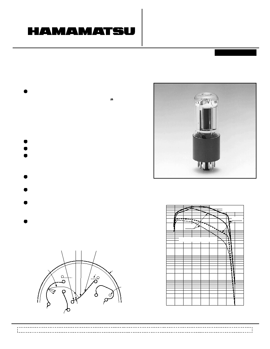
28mm (1-1/8 Inch) Diameter, 9-Stage, Side-On Type
FEATURES
lnformation furnished by HA MAM ATS U is believed to be reliabIe. However, no responsibility is assumed for possibIe inaccuracies or ommissions. Specifications are
subject to change without notice. No patent right are granted to any of the circuits described herein.
©
1994 Hamamatsu Photonics K.K.
Subject to local technical requirements and regulations, availability of products included in this promotional material may var y. Please consult with our sales office.
PHOTOMULTlPLlER TUBE
R3896
APPLICATIONS
Biomedical Analysis
Environmental Monitoring
Spectroscopy
Semiconductor Industry
High Sensitivity
Luminous ..........................................
Radiant
at 450nm (peak) .............................
at 633nm .........................................
Quantum Efficiency
at 260nm (peak) ....................................
at 633nm (peak) ....................................
Blood Analyzer, Flow Cytometer, DNA Sequencer
NOx Analyzer
Fluorescence Spectrometer, Raman Spectrometer,
UV≠VIS Spectrometer
Wafer Inspection, Particle Counter
Wide Spectral Response ............................
High Signal to Noise Ratio
Newly Designed Electro Optical Structure
525 A/lm (Typ.)
90mA/W (Typ.)
73mA/W (Typ.)
30% (Typ.)
14% (Typ.)
185 to 900nm
Figure 2: Typical Spectral Response
Figure 1: Electro Optical Structure
LIGHT
PHOTOELECTRON
TRAJECTORIES
GRILL
GLASS BULB
ANODE
9th DYNODE
PHOTOCATHODE
2nd DYNODE
1st DYNODE
TPMSC0024EA
TPMSB0049EB
100
10
1
0.1
0.01
100 200
300
400
500
600
700 800 900 1000
WAVELENGTH (nm)
CATHODE RADIANT SENSITIVITY (mA/W)
QUANTUM EFFICIENCY (%)
QUANTUM EFFICIENCY
R3896
R928
CATHODE RADIANT
SENSITIVITY
PATENT PENDING

GENERAL
Parameter
Description/Value
Unit
Spectral Response
Wavelength of Maximum Response
185 to 900
nm
nm
Photocathode
MateriaI
450
Structure
4
pF
Anode to Last Dynode
6
pF
Anode to All Other Electrodes
Minimum Effective Area
Multialkali
mm
Window Material
Weight
8 24
g
Approx. 45
Dynode
Direct Interelectrode Capacitances
Base
Supply Voltage
Between Anode and Cathode
Between Anode and Last Dynode
1250
250
0.1
Vdc
Vdc
mA
Average Anode Current
A
Ambient Temperature
UV glass
Circular-cage
Number of Stages
JEDEC No. B11-88
CHARACTERISTlCS (at 25 )
NOTES
Cathode Sensitivity
Anode Dark Current
F
(after 30min. storage in the darkness)
Anode Current Stability
J
A:
B:
C:
D:
E:
Averaged over any interval of 30 seconds
maximum.
The light source is a tungsten filament lamp
operated at a distribution temperature of 2856K.
Supply voltage is 100 volts between the cathode
and all other electrodes connected together as
anode.
The value is cathode output current when a blue
filter(Coming CS-5-58 polished to 1/2 stock
thickness) is interposed between the light source
and the tube under the same condition as Note B.
Red/White ratio is the quotient of the cathode
current measured using a red filter(Toshiba R-68)
interposed between the light source and the tube
by the cathode current measured with the filter
removed under the same conditions as Note B.
Measured with the same light source as Note B
and with the voltage distribution ratio shown in
Table 1 below.
Current Hysteresis
Voltage Hysteresis
Radiant at 254nm
Red/White Ratio
D
Blue
C
0.4
15
450nm
633nm
852nm
90
73
5.0
450nm
633nm
852nm
24.8
14.3
0.73
Anode Pulse Rise Time
G
Electron Transit Time
H
Transit Time Spread (TTS)
I
Time Response
Electrodes
K
Dy1 Dy2 Dy3 Dy4 Dy5 Dy6 Dy7 Dy8 Dy9
P
Ratio
1
1
1
1
1
1
1
1
1
1
SuppIy Voltage : 1000Vdc, K : Cathode, Dy : Dynode, P : Anode
Quantum Efficiency at 254nm
29.3
Gain
E
9.5 10
6
SuitabIe Socket
E678≠11A (option)
MAXIMUM RATINGS (Absolute Maximum Values)
Parameter
Value
Unit
PHOTOMULTlPLlER TUBE R3896
Luminous
B
475
60
525
Table 1:Voltage Distribution Ratio
≠80 to +50
Parameter
Typ.
Min.
Max.
Unit
Anode Sensitivity
Luminous
E
2.2
1.2
0.1
1.0
22
%
%
mA/W
A/lm-b
mA/W
mA/W
mA/W
ns
ns
ns
A/lm
%
%
%
%
nA
3000
5000
50
10
A/lm
F:
G:
H:
I:
J:
Measured with the same supply voltage and
voltage distribution ratio as Note E after removal of
light.
The rise time is the time for the output pulse to
rise from 10% to 90% of the peak amplitude when
the entire photocathode is illuminated by a delta
function light pulse.
The electron transit time is the interval between
the arrival of delta function light pulse at the
entrance window of the tube and the time when
the anode output reaches the peak amplitube. In
measurement, the whole photocathode is
illuminated.
Also called transit time jitter. This is the fluctuation
in electron transit time between individual pulses in
the signal photoelectron mode, and may be defined
as the FWHM of the frequency distribution of
electron transit times
Hysteresis is temporary instability in anode current
after light and voltage are applied.
(1)Current Hysteresis
The tube is operated at 750 volts with an anode
current of 1 microampere for 5 minutes. The light is
then removed from the tube for a minute. The tube is
then re-illuminated by the previous light level for a
minute to measure the variation.
(2)Voltage Hysteresis
The tube is operated at 300 volts with an anode
current of 0.1 micro-ampere for 5 minutes. The light
is then removed from the tube and the supply voltage
is quickly increased to 800 volts. After a minute, the
supply voltage is then reduced to the previous value
and the tube is re-illuminated for a minute to
measure the variation.
Hysteresis =
100(%)
lmax.
li
lmin.
TPMSB0002EA
TIME
max.
l
min.
l
i
l
ANODE
CURRENT
0
5
6
7 (minutes)
9

Figure 3: Typical Temperature Characteristics
of Dark Current
(at 1000V, after 30minutes storage)
Figure 4: Anode Luminous Sensitivity and
Gain Characteristics
Figure 5: Typical Time Response
Figure 6: Typical Temperature Coefficient
of Anode Sensitivity
TPMSB0050EA
100
10
1
0.1
≠40
≠20
0
+20
+40
TEMPERATURE (
∞
C)
ANODE DARK CURRENT (nA)
0.01
TPMSB0051EA
500
700
1000
2000
1500
GAIN
ANODE LUMINOUS SENSITIVITY (A/lm)
10
2
10
3
10
4
10
5
10
6
10
1
SUPPLY VOLTAGE (V)
GAIN (TYP.)
10
4
10
5
10
6
10
7
10
8
10
3
ANODE LUMINOUS
SENSITIVITY (MIN.)
ANODE LUMINOUS
SENSITIVITY (TYP.)
500
1000
1500
2000
TIME (ns)
SUPPLY VOLTAGE (V)
TRANSIT TIME
RISE TIME
1
100
10
TPMSB0052EA
TPMSB0053EA
WAVELENGTH (nm)
TEMPERATURE COEFFICIENT (%/ )
200
400
600
800
1000
+4.0
+1.0
-2.0
+3.0
+2.0
0
-1.0
-0.13%/
-0.25%/
PHOTOMULTlPLlER TUBE R3896
TPMS1013E03
OCT. 1994
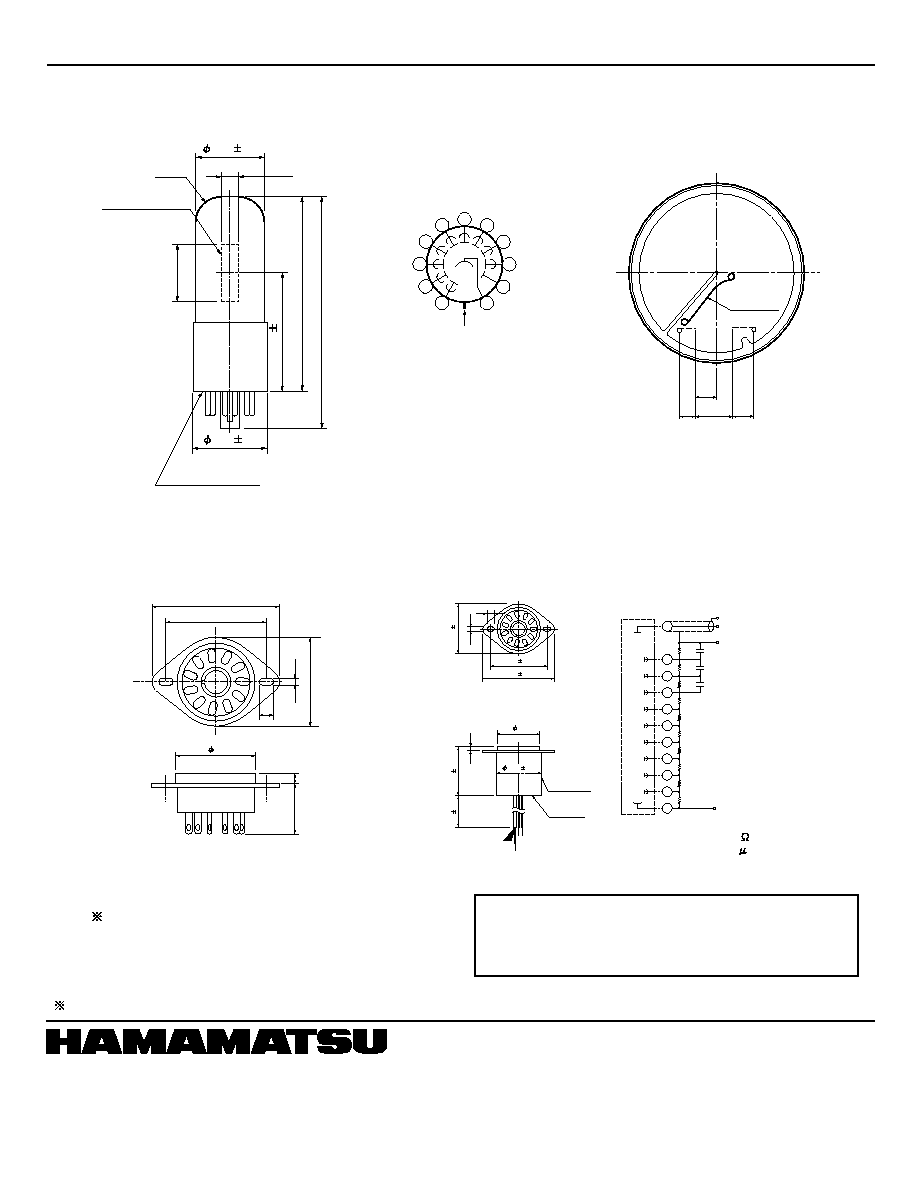
Figure 7: Dimensional Outline and Basing Diagram (Unit:mm)
Figure 8: Optional Accessories (Unit:mm)
D Type Socket Assembly E717-21
Socket E678-11A
BOTTOM VIEW
(BASING DIAGRAM)
Warning≠Personal Safety Hazards
Electrical Shock≠Operating voltages applied to this
device present a shock hazard.
Hamamatsu also provides C4900 series compact high voltage
power supplies and C6270 series DP type socket assemblies
which incorporate a DC to DC converter type high voltage
power supply.
PATENT PENDING : JAPAN 4, USA 4, EUROPE 4
POTTING
COMPOUND
TACCA0002ED
R to R10
C1 to C3
: 330k
: 0.01 F
3.5
33.0 0.3
49.0 0.3
29
38.0 0.3
4.8
41.0
0.5
450 10
5
31.0 0.5
HOUSING
(INSULATOR)
R10
R9
R8
R7
R6
R5
R4
R3
R2
R1
DY9
DY8
DY7
DY6
DY5
DY4
DY3
DY2
DY1
C3
C2
C1
SIGNAL GND
SIGNAL OUTPUT RG-174/U
(BLACK)
≠
HV
AWG22 (VIOLET)
P
K
10
POWER SUPPLY GND
AWG22 (BLACK)
SOCKET
PIN No.
PMT
9
8
7
6
5
4
3
2
1
11
TPMSA0008EA
1
2
4
3
5
7
6
8
9
10
K
DY1
DY2
DY3
DY4
DY5
DY6
DY7
DY8
DY9
P
DIRECTION OF LIGHT
28.5 1.5
8MIN.
T9
BULB
PHOTOCATHODE
24MIN.
49.0 2.5
80MAX.
94MAX.
32.2 0.5
11 PIN BASE
JEDEC No. B11-88
11
PHOTO -
CATHODE
3.25
2.5
6.0
3.5
TPMSA0009EA
Cross Section
TACCA0064EA
33
5
49
3.5
38
29
4
18
HAMAMATSU PHOTONICS K.K., Electoron Tube Center
314-5, Shimokanzo, Toyooka-village, Iwata-gun, Shizuoka-ken, 438-0193, Japan, Telephone: (81)539/62-5248, Fax: (81)539/62-2205
U.S.A.: Hamamatsu Corporation: 360 Foothill Road, Bridgewater. N.J. 08807-0910, U.S.A., Telephone: (1)908-231-0960, Fax: (1)908-231-1218
Germany: Hamamatsu Photonics Deutschland GmbH: Arzbergerstr. 10, D-82211 Herrsching am Ammersee, Germany, Telephone: (49)8152-375-0, Fax: (49)8152-2658
France: Hamamatsu Photonics France S.A.R.L.: 8, Rue du Saule Trapu, Parc du Moulin de Massy, 91882 Massy Cedex, France, Telephone: (33)1 69 53 71 00, Fax: (33)1 69 53 71 10
United Kingdom: Hamamatsu Photonics UK Limted: Lough Point, 2 Gladbeck Way, Windmill Hill, Enfield, Middlesex EN2 7JA, United Kingdom, Telephone: (44)181-367-3560, Fax: (44)181-367-6384
North Europe: Hamamatsu Photonics Norden AB: F‰rˆgatan 7, S-164-40 Kista Sweden, Telephone: (46)8-703-29-50, Fax: (46)8-750-58-95
Italy: Hamamatsu Photonics Italia: S.R.L.: Via Della Moia, 1/E, 20020 Arese, (Milano), Italy, Telephone: (39)2-935 81 733, Fax: (39)2-935 81 741