 | –≠–ª–µ–∫—Ç—Ä–æ–Ω–Ω—ã–π –∫–æ–º–ø–æ–Ω–µ–Ω—Ç: V2697U | –°–∫–∞—á–∞—Ç—å:  PDF PDF  ZIP ZIP |

18mm DIA. PHOTOCATHODE
PROXIMITY FOCUSED
IMAGE INTENSIFIER
V2697U
Figure 1: Typical Spectral Response
........................
Subject to local technical requirements and regulations, availability of products included in this promotional material may vary. Please consult with our sales office.
Information furnished by HAMAMATSU is believed to be reliable. However, no responsibility is assumed for possible inaccuracies or omissions.
Specifications are subject to change without notice. No patent rights are granted to any of the circuits described herein. © 1998 Hamamatsu Photonics K. K.
Proximity Focused,
High Image Quality, Wide Spectral Response, No Image Distortion
For Scientific Applications
FEATURES
q
Compact size and lightweight
q
No image distortion
q
High sensitivity
60 mA/W at 430 nm
q
Wide spectral response
q
High gain
APPLICATIONS
q
Low-light-level multichannel spectrophotometer
(with a linear photodiode array, etc.)
Raman spectroscopy, Emission spectroscopy, etc.
q
Low-light-level imaging
(with image sensors such as vidicon, CCD, etc.)
Microscope, Low-light-level TV, Streak camera, etc.
GENERAL
Parameter
Description
Unit
Spectral Response (See Fig. 1)
160 to 900
nm
Wavelength of Maximum Response
430
nm
Photocathode
A
Material
Multialkali
≠
Minimum Effective Diameter
18
mm
Input Window Material
Synthetic silica
≠
MCP
Single stage
≠
Output Window Material
Fiber optic plate
≠
Phosphor Screen Material (See Fig. 8)
B
P-43
≠
Case Material
Poly Oxy Methylene (POM)
≠
Lead Wire Cover
Teflon
≠
Weight
Approx. 80
g
A
Other photocathode materials may be available upon your request.
Please contact with our sales office.
B
The P-20 model is also available for the above applications. The
characteristics are the same except for Fig.8, the phosphor spectral
emission.
10
2
10
1
10
0
10
≠1
100 200 300 400 500 600 700 800 900 1000
WAVELENGTH (nm)
CATHODE RADIANT SENSITIVITY (mA/W)
QUANTUM EFFICIENCY (%)
RADIANT SENSITIVITY
QUANTUM EFFICIENCY
TII B0013EB

MAXIMUM RATINGS
Parameter
Value
Unit
q
Supply Voltage
Photocathode and MCP-In
230
Vdc
MCP-In and MCP-Out
C
700 to 1000
Vdc
MCP-Out and Phosphor Screen
6100
Vdc
q
Maximum Light Level
Luminous
0.01
lx
Radiant at 430 nm
3
◊
10
-9
W/cm
2
q
Temperature
Storage
≠ 55 to +65
∞C
Operating
≠ 20 to +40
∞C
Shock
12
∞C/min
CHARACTERISTICS
Parameter
Min.
Typ.
Max.
Unit
q
Photocathode Sensitivity
Luminous
D
100
170
≠
µ
A/lm
Radiant at 200 nm (See Fig. 1)
≠
30
≠
at 430 nm
≠
60
≠
at 550 nm
≠
41
≠
mA/W
at 700 nm
≠
22
≠
at 800 nm
≠
10
≠
Quantum Efficiency at 430 nm
≠
17
≠
%
q
Light Gain (See Fig. 5, Fig. 6)
Luminous Gain
E
7000
12000
≠
lm/m
2
lx
I
Radiant Emittance Gain at 430 nm
F
≠
8700
≠
W/m
2
W/m
2
q
EBI (Equivalent Background Input) (See Fig. 5)
G
Luminous
≠
1
◊
10
≠11
4
◊
10
≠11
lm/cm
2
Radiant at 430 nm
≠
3
◊
10
≠14
≠
W/cm
2
Limitting Resolution (See Fig. 4)
H
25
30
≠
lp/mm
Magnification
≠
1
≠
≠
Distortion
≠
0
≠
≠
RECOMMENDED OPERATION
Parameter
Value
Unit
q
Supply Voltage
Photocathode and MCP-In (Vk)
150 to 200
Vdc
MCP-In and MCP-Out (V
MCP
)
C
500 to 1000
Vdc
MCP-Out and Phosphor Screen (Vs)
5000 to 6000
Vdc
Figure 2: Operating Diagram (example)
NOTE: ∑ A separate power supply can be supplied on request.
∑ GND potential can be assigned to any electrode.
Figure 3: Example of Coupling to Imaging Device
PROXIMITY FOCUSED IMAGE INTENSIFIER V2697U
NOTE: The transparent conductive film (NESA cooting) is required on
the output FOP of the tube or the coupling FOP to prevent the
induction of noise if the tube will be operated by other than
ground potential at the screen.
V2697U
PHOTODIODE ARRAY or
SOLID STATE IMAGE SENSOR
(MOS, PCD, CCD, etc.)
TRANSPARENT
CONDUCTIVE FILM
FIBER OPTIC PLATE
TII C0017EC
TII C0014EB
NOTES
C
: The maximum supply voltage and recommended
supply voltage for the MCP-In and MCP-Out are
noted on the test data sheet when the product is
delivered. Please refer to the test data sheet for
these values.
D
: The light source is a tungsten filament lamp
operated at a distribution temperature of
2856 K.
Supply voltage is 200 volts between the pho-
tocathode and all other electrodes (MCP-In,
MCP-Out, Phosphor Screen) connected to-
gether as anode.
E
: The luminous gain has relation to the screen
luminance Lo (cd/m
2
) and the illuminance Ei
(lx) incident on the photocathode, and ex-
pressed by:
Luminous Gain =
∑
The supply voltages are as follows.
Photocathode and MCP-In ............ 200 Vdc
MCP-In and MCP-Out ..... 500 to 1000 Vdc
MCP-Out and Phosphor Screen . 6000 Vdc
F
: The ratio of the phosphor screen radiant
emittance in watts per square meter (W/m
2
) to
the irradiance (W/m
2
) on the photocathode.
The supply voltages are the same as
E
.
G
: The inherent background noise of an image
intensifier is normally specified as the input
illuminance (or irradiance) required to produce
a luminous emittance from the phosphor
screen, equal to that obtained when the input
illuminance is zero.
This indicates the lower limit of detectable
illuminance of an image intensifier.
H
: The measure of the ability to detect white and
black stripes in an image formed at the photo-
cathode, in terms of line pairs (lp) (one black
and one white stripe) per millimeter. This is
the value at an MTF (Modulation Transfer
Function) of 5%.
I
: 1 lm/m
2
= 0.0929 ft-L
1 lx = 0.0929 ft-c
1 lm/m
2
lx = 1 ft-L/ft-c
Lo
Ei
PHOTOCATHODE
MCP
PHOSPHOR
SCREEN
(GREEN)
(VIOLET)
(BLACK)
(RED)
V
V
V
K
MCP
S
150 to 200V
500 to 1000V
5000 to
6000V
0
10
20
30
40
SPATIAL RESOLUTION (Lp/mm)
100
80
60
40
20
0
MTF (%)
10
1
500
600
700
800
900
MCP VOLTAGE(V)
LUMINOUS GAIN (lm/m
2
/lx)
10
-12
EBI (lm/cm
2
)
10
-11
10
-10
10
-9
10
-8
10
2
10
3
10
4
10
5
EBI
LUMINOUS GAIN
10
2
10
1
10
0
10
≠1
10
≠2
10
≠3
10
≠4
10
≠5
10
≠9
10
≠8
10
≠7
10
≠6
10
≠5
10
≠4
10
≠3
10
≠2
10
≠1
INPUT ILLUMINANCE (lx)
LUMINOUS EMITTANCE (lm/m
2
)
10
3
G=7
◊
10
3
G=2
◊
10
4
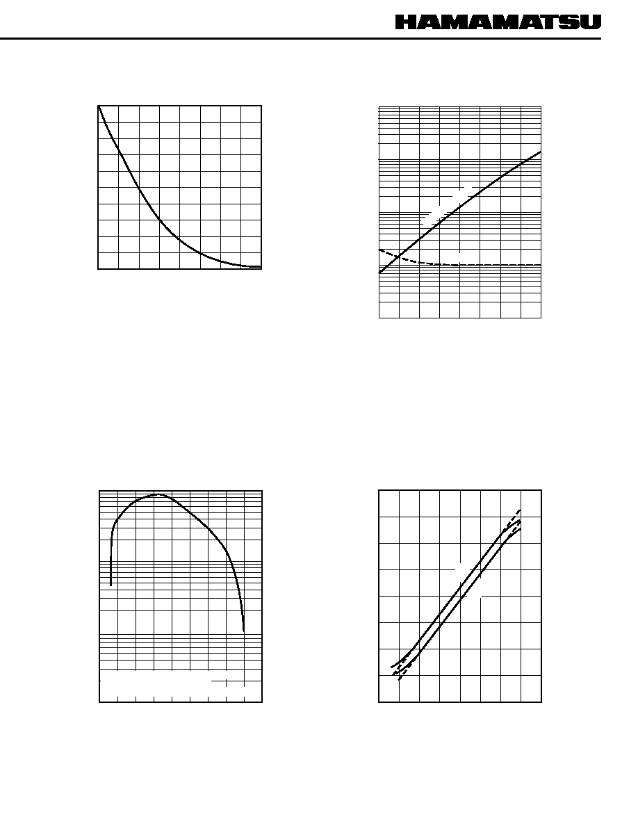
Figure 4: Typical MTF
Figure 5: Typical Luminous Gain and EBI
vs. MCP Voltage
TII B0014EC
TII B0015EF
Figure 6: Radiant Emittance Gain vs. Wavelength
Figure 7: Typical Photocathode Illuminance
vs. Phosphor Screen Luminous Emittance
TII B0016EA
TII B0017ED
10
3
10
2
10
1
10
4
RADIANT EMITTANCE GAIN (W/m
2
/W/m
2
)
PHOTOCATHODE AND MCP-IN=200 Vdc
MCP-IN AND MCP-OUT=900 Vdc
MCP-OUT AND PHOSPHOR SCREEN=6000 Vdc
100 200 300 400
500 600 700 800
900 1000
WAVELENGTH (nm)
NOTE: Radiant Emittance Gain based on the emittance
energy of phosphor screen P-43: 1cd/m
2
=6.4
◊
10
-3
W/m
2
.

Figure 8: Typical Phosphor Spectral Emission
Figure 9: Dimensional Outline (Unit: mm)
PROXIMITY FOCUSED IMAGE INTENSIFIER V2697U
Warning ≠ Personal Safety Hazards
Electrical Shock ≠ Operating voltages
applied to this device present a shock hazard.
TII B0062EB
TII A0010EC
5
A high-speed gated image intensifier (V3063U) is
also available in the same configuration.
5
Case is insulated from other electrodes.
Withstand voltage of package and leads is more
than 10kV. When fixing the V2697U, use a material
which withstands a voltage sufficiently higher
than is applied to the tube.
100
80
60
40
20
0
450
400
550
650
500
700
RELATIVE INTENSITY (%)
WAVELENGTH (nm)
600
P-43
HAMAMATSU PHOTONICS K.K., Electron Tube Center
314-5, Shimokanzo, Toyooka-village, Iwata-gun, Shizuoka-ken, 438-0193, Japan, Telephone: (81)539/62-5248, Fax: (81)539/62-2205
U.S.A.: Hamamatsu Corporation: 360 Foothill Road, Bridgewater, N.J. 08807-0910, U.S.A., Telephone: (1)908-231-0960, Fax: (1)908-231-1218
Germany: Hamamatsu Photonics Deutschland GmbH: Arzbergerstr. 10, D-82211 Herrsching am Ammersee, Germany, Telephone: (49)8152-375-0, Fax: (49)8152-2658
France: Hamamatsu Photonics France S.A.R.L.: 8, Rue du Saule Trapu, Parc du Moulin de Massy, 91882 Massy Cedex, France, Telephone: (33)1 69 53 71 00, Fax: (33)1 69 53 71 10
United Kingdom: Hamamatsu Photonics UK Limited: Lough Point, 2 Gladbeck Way, Windmill Hill, Enfield, Middlesex EN2 7JA, United Kingdom, Telephone: (44)181-367-3560, Fax: (44)181-367-6384
North Europe: Hamamatsu Photonics Norden AB: F‰rˆgatan 7, S-164-40 Kista, Sweden, Telephone: (46)8-703-29-50, Fax: (46)8-750-58-95
Italy: Hamamatsu Photonics Italia S.R.L.: Via Della Moia, 1/E 20020 Arese, (Milano), Italy, Telephone: (39)2-935 81 733, Fax: (39)2-935 81 741
TII 1007E04
MAR. 1998 SI
Printed in Japan (500)
EFFECTIVE PHOTOCATHODE DIAMETER
18 ∞
18 ∞
+0
≠0.3
BLACK
VIOLET
GREEN
RED
2.0
±
0.2
5.5
±
0.1
0.5
±
0.2
23.0
±
0.3
INPUT WINDOW
PHOTOCATHODE
OUTPUT WINDOW
(FIBER OPTIC PLATE)
LEAD LENGTH
200 MIN.
LEAD
GREEN
VIOLET
BLACK
RED
(TEFLON COVER)
(PHOTOCATHODE)
(MCP-INPUT)
(MCP-OUTPUT)
(PHOSPHOR SCREEN)
EFFECTIVE
PHOSPHOR SCREEN DIAMETER
INPUT VIEW
OUTPUT VIEW
18 MIN.
45.0
19
21.8
18 MIN.