 | –≠–ª–µ–∫—Ç—Ä–æ–Ω–Ω—ã–π –∫–æ–º–ø–æ–Ω–µ–Ω—Ç: HTC150CDC | –°–∫–∞—á–∞—Ç—å:  PDF PDF  ZIP ZIP |

HI HIGH TECH
CHIPS, INC.
12/03/99
1
PDIP, SOIC
1
8
2
7
3
6
4
5
HTC150A, HTC150B,
HTC150C, HTC150D
LED FLASHERS
1.0 General description.
This circuit is designed to work as led flasher. LED's
sequentially turn on and off according to part used. D0 and D1
inputs are used to control flashing frequency. There are four
different frequencies selectable. See D[0:1] versus frequency
table. HTC150 Can control up to 32 LED's (eight LED's per
output @ 3mA each).
Features
∑
Minimal external components.
∑
Easy selection of alternating frequency.
∑
Predictability and design ease.
Pin out description.
Abbreviations used: O - output, I - input, P - power.
Pin number Name
I / O
Description
Notes
1
VDD
P
Power
+2.5V to +5.5V
2
LED 1
O
Output for LED1
Can source up to 25mA
3
LED 2
O
Output for LED2
Can source up to 25mA
4
D0
I
Frequency selector D0
Tie it to VDD or GND(see table below)
5
D1
I
Frequency selector D1
Tie it to VDD or GND(see table below)
6
LED 3
O
Output for LED3
Can source up to 25mA
7
LED 4
O
Output for LED4
Can source up to 25mA
8
GND
P
Ground
Connects to digital ground.
Frequency selection per D[0:1]
Abbreviations used: 0 ≠ connection to GND, 1 ≠ connection to VDD.
D1
D0
Switching frequency
0
0
2Hz
0
1
4Hz
1
0
8Hz
1
1
16Hz
Please note that those values are for reference only. Actual frequency can vary up to 10 percent
depending upon VDD voltage and operational temperature.
VDD GND
LED1 LED4
LED2 LED3
D0 D1

HI HIGH TECH
CHIPS, INC.
12/03/99
2
2.0 Functional description.
HTC150 has several variations determined by part number. Common to all models of HTC150 is
alternating frequency selection and pin-out. Please refer to "Typical connection diagram" used as
reference. Frequency is changed when state of D[0:1] input pins change. Refer to "Frequency
selection per D[0:1]" table for frequency selection. Note that Dip Switch could be omitted by hard
wiring D[0:1] inputs to GND or VDD. This section describes operation of each HTC150 model
separately. Each part uses different alternating algorithm.
HTC150A
States:
1. LED1 is turned on and all others are off.
2. LED2 is turned on and all others are off.
3. LED3 is turned on and all others are off.
4. LED4 is turned on and all others are off.
State is changed at frequency selected by D[0:1].
HTC150B (Ping-Pong)
States:
1. LED1 is turned on and all others are off.
2. LED2 is turned on and all others are off.
3. LED3 is turned on and all others are off.
4. LED4 is turned on and all others are off.
5. LED3 is turned on and all others are off.
6. LED2 is turned on and all others are off.
State is changed at frequency selected by D[0:1].
HTC150C (Accumulate)
States:
1. LED1 is turned on and all others are off.
2. LED2 is turned on and all others are off.
3. LED3 is turned on and all others are off.
4. LED4 is turned on and all others are off.
5. LED1 and LED4 are turned on and all others are off.
6. LED2 and LED4 are turned on and all others are off.
7. LED3 and LED4 are turned on and all others are off.
8. LED1 and LED4 and LED3 are turned on and all others are off.
9. LED2 and LED4 and LED3 are turned on and all others are off.
10. All LED's are turned on.
11. All LED's are turned off.
State is changed at frequency selected by D[0:1].
HTC150D (Binary count)
States of LED's is similar to four bit binary counter.
State is changed at frequency selected by D[0:1].

HI HIGH TECH
CHIPS, INC.
12/03/99
3
The circuit will change the flashing frequency as soon as the DO or D1 input pin state is changed.
From that time next LED's start flashing at new frequency. The first LED starts over with the new
frequency and it continues until the D0 or D1 state is changed again.
3.0 Typical connection diagram.
5V
5V
5V
HTC150
LED 1
2
LED 2
3
D0
4
VDD
1
D1
5
LED 4
7
LED 3
6
GND
8
SW
1
2
4
3
R1
10K
R2
10K
R3
333
R6
333
R4
333
R5
333
D4
LED
D3
LED
D2
LED
D1
LED

HI HIGH TECH
CHIPS, INC.
12/03/99
4
4.0 Electrical characteristics.
Operational Voltage.
+2.5 to +5.5V
Current consumption with no load attached
3 mA
1
LEDx
output low voltage (5mA load)
0.4V
1
LEDx
output low voltage (25mA load)
0.75V
1
LEDx
output high voltage (5mA source)
VDD-0.7V
1
LEDx
output source current max
25mA
1
LEDx
output sink current max
25mA
1
NOTES:
1. Those values are characterized but not tested.
5.0 Ordering information.
H
T
C
1
5
0
X
X
X
OPTIONAL: Temperature range:
C = 0
o
C to +70
o
C , I = - 40
o
C to + 85
o
C.
PACKAGE:
S ≠ 200 mil SOIC
D ≠ 300 mil PDIP.
Model
A (sequential), B (Ping-Pong),
C (Accumulate), D (Binary count)
PART NUMBER.
HI HIGH TECH
CHIPS, INC.
12/03/99
5
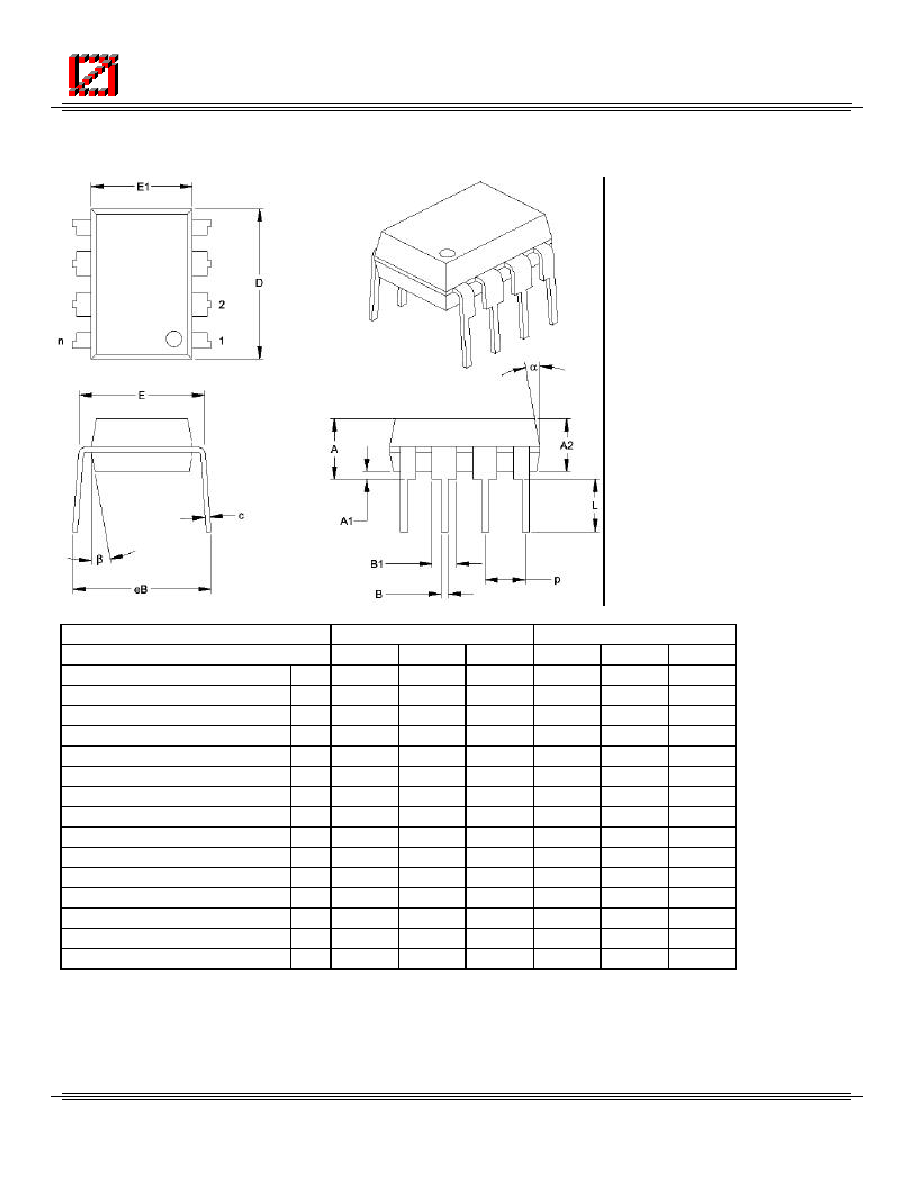
6.0
Mechanical information
.
8-Lead Plastic Dual In-line (P) ≠ 300 mil (PDIP)
Units
INCHES*
MILLIMETERS
Dimension Limits
MIN
NOM
MAX
MIN
NOM
MAX
Number of Pins
n
8
8
Pitch
P
.100
2.54
Top of Seating Plane
A
.140
.155
.170
3.56
3.94
4.32
Molded Package Thickness
A2
.115
.130
.145
2.92
3.30
3.68
Base of Seating Plane
A1
.015
0.38
Shoulder to Shoulder Width
E
.300
.313
.325
7.62
7.94
8.26
Molded Package Width
E1
.240
.250
260
6.10
6.35
6.60
Overall Length
D
.360
.373
.385
9.14
9.46
9.78
Tip to Seating Plane
L
.125
.130
.135
3.18
3.30
3.43
Lead Thickness
c
.008
.012
.015
0.20
0.29
0.38
Upper Lead Width
B1
.045
.058
.070
1.14
1.46
1.78
Lower Lead Width
B
.014
.018
.022
0.36
0.46
0.56
Overall Row Spacing
eB
.310
.370
.430
7.87
9.40
10.92
Mold Draft Angle Top
5
10
15
5
10
15
Mold Draft Angle Bottom
5
10
15
5
10
15
*Controlling Parameter
Notes:
Dimensions D and E1 do not include mold flash protrusions. Mold flash or
protrusions shell not exceed .010" (0.254mm)per side.
JEDEC Equivalent:MS-001