
2SB1103
Silicon PNP Triple Diffused
Application
Low frequency power amplifier
Outline
TO-220AB
4.0 k
(Typ)
200
(Typ)
1
2
3
1. Base
2. Collector
(Flange)
3. Emitter
1
2
3
I
D
2SB1103
2
Absolute Maximum Ratings (Ta = 25∞C)
Item
Symbol
Ratings
Unit
Collector to emitter voltage
V
CBO
≠60
V
Collector to emitter voltage
V
CEO
≠60
V
Emitter to base voltage
V
EBO
≠7
V
Collector current
I
C
≠8
A
Collector peak current
I
C(peak)
≠12
A
Collector power dissipation
P
C
*
1
40
W
Junction temperature
Tj
150
∞
C
Storage temperature
Tstg
≠55 to +150
∞
C
C to E diode forward current
I
D
*
1
8
A
Note:
1. Value at T
C
= 25
∞
C.
Electrical Characteristics (Ta = 25∞C)
Item
Symbol
Min
Typ
Max
Unit
Test conditions
Collector to emitter breakdown
voltage
V
(BR)CEO
≠60
--
--
V
I
C
= ≠25 mA, R
BE
=
Emitter to base breakdown
voltage
V
(BR)EBO
≠7
--
--
V
I
E
= ≠50 mA, I
C
= 0
Collector cutoff current
I
CBO
--
--
≠100
µ
A
V
CB
= ≠60 V, I
E
= 0
I
CEO
--
--
≠10
µ
A
V
CE
= ≠50 V, R
BE
=
DC current tarnsfer ratio
h
FE
1000
--
20000
V
CE
= ≠3 V, I
C
= ≠4 A*
1
Collector to emitter saturation
voltage
V
CE(sat)1
--
--
≠1.5
V
I
C
= ≠4 A, I
B
= ≠8 mA*
1
V
CE(sat)2
--
--
≠3.0
I
C
= ≠8 A, I
B
= ≠80 mA*
1
Base to emitter saturation
voltage
V
BE(sat)1
--
--
≠2.0
V
I
C
= ≠4 A, I
B
= ≠8 mA*
1
V
BE(sat)2
--
--
≠3.5
I
C
= ≠8 A, I
B
= ≠80 mA*
1
C to E diode forward voltage
V
D
--
--
3.0
V
I
D
= 8 A*
1
Turn on time
t
on
--
0.5
--
µ
s
I
C
= ≠4 A,
Storage time
t
stg
--
3.0
--
I
B1
= ≠I
B2
= ≠8 mA
Fall time
t
f
--
1.0
--
Note:
1. Pulse Test.
2SB1103
3
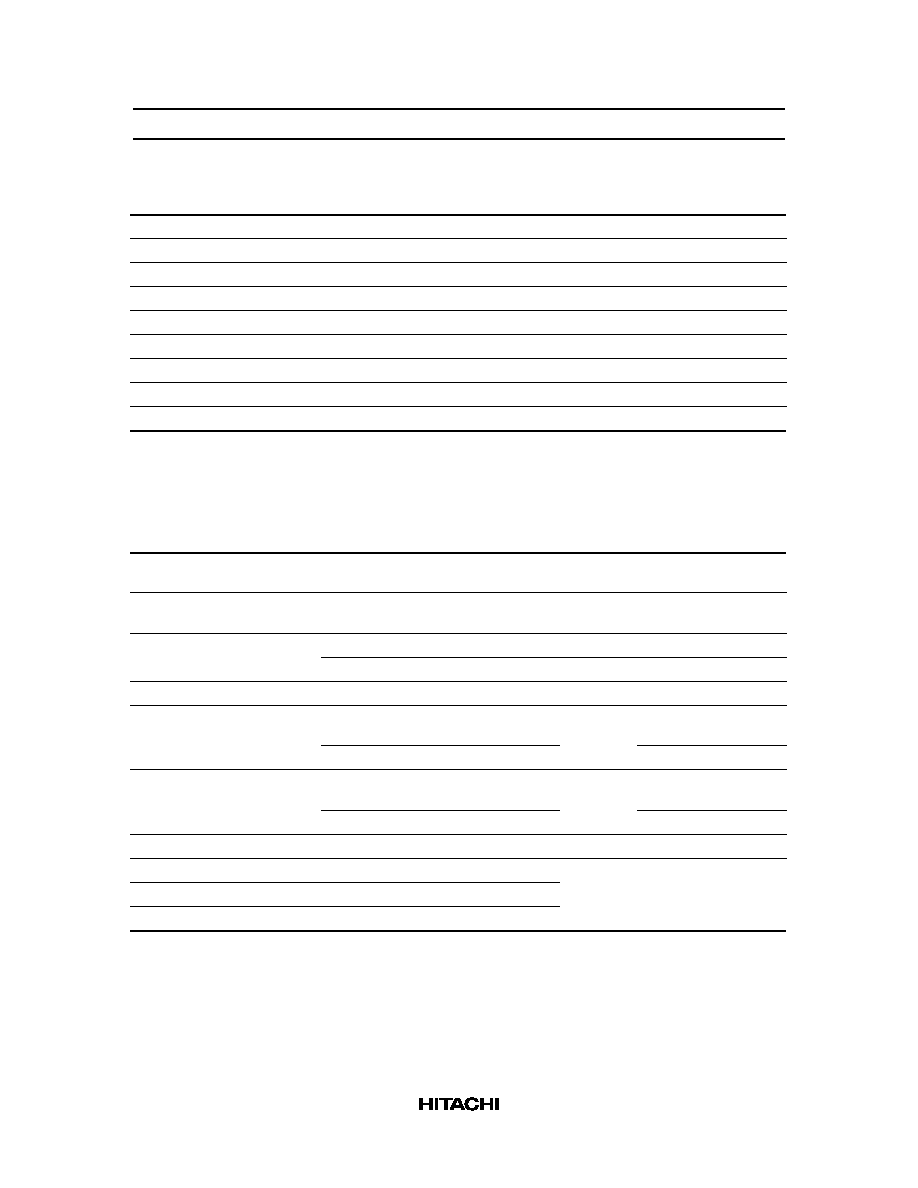
Maximum Collector Dissipation
Curve
60
40
20
0
50
100
150
Case temperature T
C
(
∞
C)
Collector power dissipation P
C
(W)
Area of Safe Operation
≠10
≠3
≠1.0
≠0.3
Collector current I
C
(A)
≠0.1
≠0.03
≠3
≠10
≠100
≠30
≠300
Collector to emitter voltage V
CE
(V)
Ta = 25
∞
C
1 Shot Pulse
i
C(peak)
1
µ
s
I
C(max)
DC Operation(T
C
= 25
∞
C)
PW = 10 ms
1 ms
100
µ
s
2S B1103
2S B1104
2SB1103
4
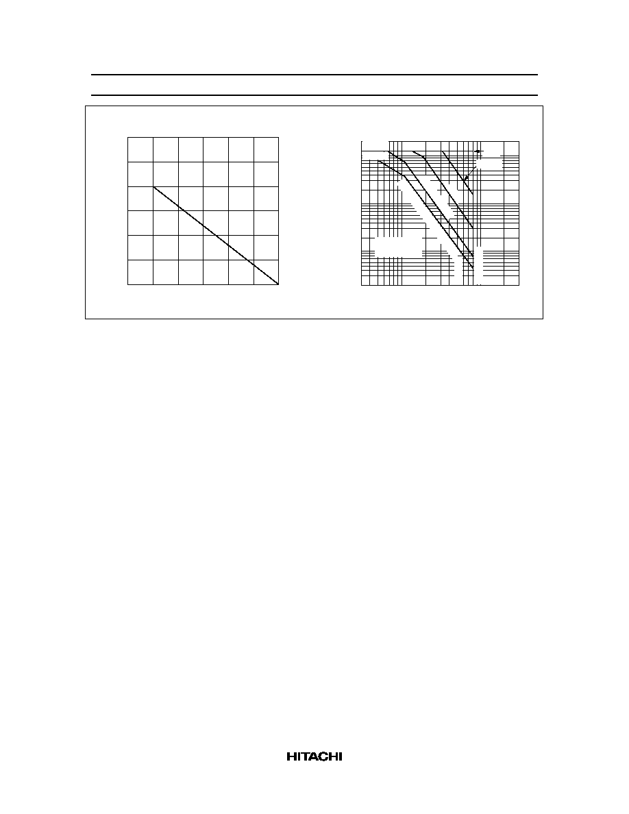
Typical Output Characteristics
I
B
= 0
≠0.5 mA
≠1.0
≠1.5
≠10
≠8
≠6
≠4
≠2
0
≠1
Collector current I
C
(A)
≠2
Collector to emitter voltage V
CE
(V)
≠3
≠5
≠4
P
C
= 40 W
≠2.5
≠3.0
≠2.0
T
C
= 25
∞
C
DC Current Transfer Ratio vs.
Collector Current
30,000
10,000
3,000
1,000
300
100
30
≠0.1
≠0.3
DC current transfer ratio h
FE
≠1.0
Collector current I
C
(A)
≠3
≠10
V
CE
= ≠3 V
Pulse
Ta = 75
∞
C
≠25
∞
C
25
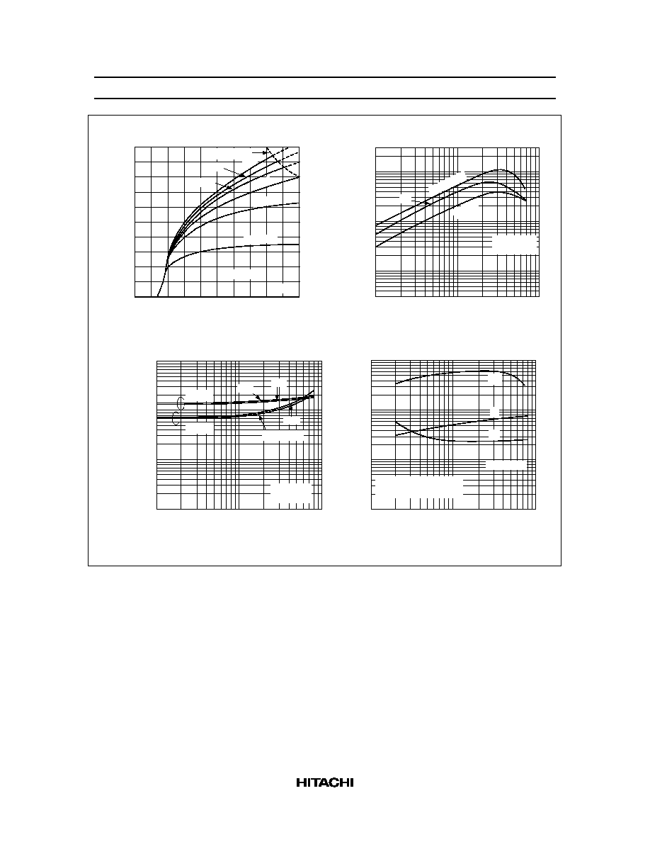
Saturation Voltage vs.
Collector Current
T
a
= 25
∞
C
Pulse
≠10
≠3
≠1.0
≠0.3
Collector to emitter saturation voltage V
CE(sat)
(V)
Base to emitter saturation voltage V
BE(sat)
(V)
≠0.03
≠0.1
≠0.01
≠0.1
Collector current I
C
(A)
≠0.3
≠1.0
≠3
≠10
V
BE(sat)
V
CE(sat)
500
500
200
I
C
/
I
B
= 200
Switching Time vs. Collector Current
Switching time t (
µ
s)
10
3
1.0
0.3
0.1
0.03
0.01
≠0.1
≠0.3
≠1.0
Collector current I
C
(A)
≠3
≠10
t
f
t
on
t
stg
V
CC
= ≠30V
I
C
= 100 I
B1
= ≠100 I
B2
Ta = 25
∞
C
