 | –≠–ª–µ–∫—Ç—Ä–æ–Ω–Ω—ã–π –∫–æ–º–ø–æ–Ω–µ–Ω—Ç: 2SC4046 | –°–∫–∞—á–∞—Ç—å:  PDF PDF  ZIP ZIP |
2SC4046
Silicon NPN Epitaxial
Application
High voltage amplifier
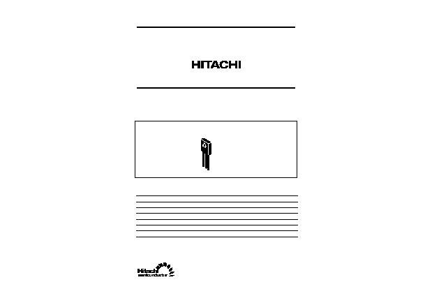
Outline
1. Emitter
2. Collector
3. Base
TO-126 MOD
1
2
3
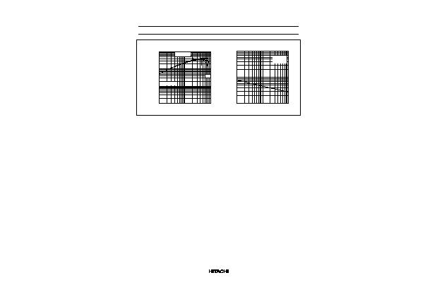
Absolute Maximum Ratings (Ta = 25∞C)
Item
Symbol
Ratings
Unit
Collector to base voltage
V
CBO
120
V
Collector to emitter voltage
V
CEO
120
V
Emitter to base voltage
V
EBO
5
V
Collector current
I
C
0.2
A
Collector power dissipation
P
C
*
1
8
W
Junction temperature
Tj
150
∞
C
Storage temperature
Tstg
≠55 to +150
∞
C
Note:
1. Value at T
C
= 25
∞
C

2SC4046
2
Electrical Characteristics (Ta = 25∞C)
Item
Symbol
Min
Typ
Max
Unit
Test conditions
Collector to base breakdown
voltage
V
(BR)CBO
120
--
--
V
I
C
= 10
µ
A, I
E
= 0
Collector to emitter breakdown
voltage
V
(BR)CEO
120
--
--
V
I
C
= 1 mA, R
BE
=
Emitter to base breakdown
voltage
V
(BR)EBO
5
--
--
V
I
E
= 10
µ
A, I
C
= 0
Collector cutoff current
I
CBO
--
--
10
µ
A
V
CB
= 80 V, I
E
= 0
DC current transfer ratio
h
FE
*
1
250
--
800
V
CE
= 5 V, I
C
= 10 mA
Base to emitter voltage
V
BE
--
--
1.0
V
Collector to emitter saturation
voltage
V
CE(sat)
--
--
1.0
V
I
C
= 200 mA, I
B
= 20 mA
Gain bandwidth product
f
T
--
350
--
MHz
V
CE
= 10 V, I
C
= 50 mA
Collector output capacitance
Cob
--
3.5
--
pF
V
CB
= 30 V, f = 1 MHz, I
E
= 0
Note:
1. The 2SC4046 is grouped by h
FE
as follows.
Grade
D
E
h
FE
250 to 500
400 to 800
0
50
150
100
Case Temperature T
C
(
∞
C)
Collector power dissipation Pc (W)
Maximum Collector Dissipation Curve
4
6
10
2
8
12
0.01
0.1
1.0
Collector to emitter Voltage V
CE
(V)
Collector Current I
C
(A)
1
10
100
1,000
Area of Safe Operation
PW = 1 ms
DC Operation
T
C
= 25
∞
C
Single Pulse
Ta = 25
∞
C
(25 V, 0.4 A)
(80 V, 0.125 A)
(120 V, 0.055 A)
(120 V, 0.05 A)
(80 V, 0.1 A)

2SC4046
3
Collector to emitter Voltage V
CE
(V)
Collector Current I
C
(mA)
0
Typical Output Characteristics
4
8
12
18
40
60
80
100
120
20
20
40
60
80
100
I
B
= 0
20
µ
A
10
100
1,000
Collector current I
C
(mA)
DC current transfer ratio h
FE
1
10
100
1,000
DC Current Transfer Ratio vs.
Collector Current
Ta = 75
∞
C
25
≠25
V
CE
= 10 V
Pulse Test
0.1
1.0
10
Collector current I
C
(mA)
Base to emitter voltage
V
BE
(V)
1
10
100
1,000
Base to Emitter Voltage
vs. Collector Current
Ta = ≠25
∞
C
75
25
V
CE
= 10 V
Pulse Test
0.01
0.1
1.0
10
Collector current I
C
(mA)
Collector to emitter saturation voltage
V
CE (sat)
(V)
1
10
100
1,000
Collector to Emitter Saturation
Voltage vs. Collector Current
≠25
25
Ta = 75
∞
C
I
C
/I
B
= 10
Pulse Test
2SC4046
4
1
10
100
1,000
Collector current I
C
(mA)
Gain bandwidth product f
T
(MHz)
1
2
5
10
20
50
100
Gain Bandwidth Product vs.
Collector Current
V
CE
= 20 V
Pulse Test
10
5
1
2
5
10
20
50
100
Collector to base voltage V
CB
(V)
Collector output capacitance C
ob
(pF)
1
2
5
10
20
50
100
Collector Output Capacitance vs.
Collector to Base Voltage
f
= 1 MHz
I
E
= 0

3.1
+0.15
≠0.1
8.0
±
0.5
2.3
±
0.3
1.1
3.7
±
0.7
11.0
±
0.5
15.6
±
0.5
0.8
2.29
±
0.5
2.29
±
0.5
0.55
1.2
2.7
±
0.4
120
∞
120
∞
120
∞
Hitachi Code
JEDEC
EIAJ
Weight (reference value)
TO-126 Mod
--
--
0.67 g
Unit: mm