HD74AC153
Dual 4-Input Multiplexer
Description
The HD74AC153 is a high-speed dual 4-input multiplexer with common select inputs and individual
enable inputs for each section. It can select two lines of data from four sources. The two buffered outputs
present data in the true (noninverted) form. In addition to multiplexer operation, the HD74AC153 can act
as a function generator and generate any two functions of three variables.
Feature
·
Outputs Source/Sink 24 mA
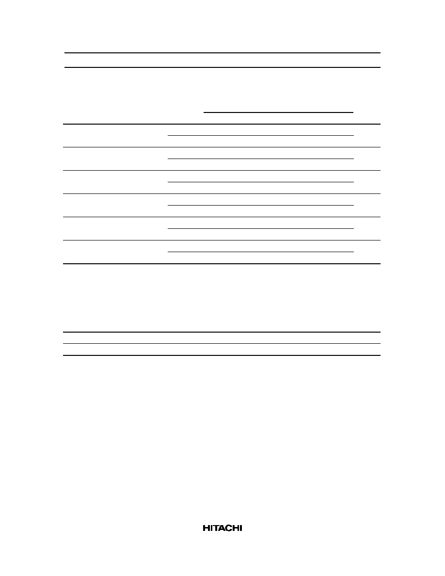
Pin Arrangement
1
2
3
4
5
6
7
8
16
15
14
13
12
11
10
9
E
a
S
1
I
3a
I
2a
I
1a
Z
a
I
0a
GND
V
CC
E
b
S
0
I
3b
I
2b
I
1b
I
0b
Z
b
(Top view)
HD74AC153
2
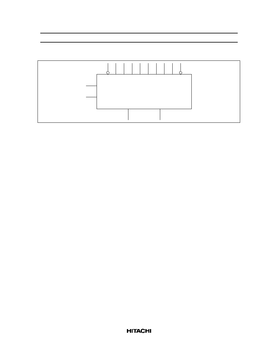
Logic Symbol
E
a
Z
a
S
0
S
1
Z
b
I
0a
I
1a
I
2a
I
3a
I
0b
I
1b
I
2b
I
3b
E
b
Pin Names
I
0a
to I
3a
Side A Data Inputs
I
0b
to I
3b
Side B Data Inputs
S
0
, S
1
Common Select Inputs
E
a
Side A Enable Input
E
b
Side B Enable Input
Z
a
Side A Output
Z
b
Side B Output
Functional Description
The HD74AC153 is a dual 4-input multiplexer. It can select two bits of data from up to four sources under
the control of the common Select inputs (S
0
, S
1
). The two 4-input multiplexer circuits have individual
active-Low Enables (
E
a
,
E
b
) which can be used to strobe the outputs independently. When the Enables (
E
a
,
E
b
) are High, the corresponding outputs (Z
a
, Z
b
) are forced Low. The HD74AC153 is the logic
implementation of a 2-pole, 4-position switch, where the position of the switch is determined by the logic
levels supplied to the two Select inputs. The logic equations for the outputs are shown below.
Z
a
=
E
a
·(I
0a
·
S
1
·
S
0
+ I
1a
·
S
1
·S
0
+ I
2a
·S
1
·
S
0
+ I
3a
·S
1
·S
0
)
Z
b
=
E
b
·(I
0b
·
S
1
·
S
0
+ I
1b
·
S
1
·S
0
+ I
2b
·S
1
·
S
0
+ I
3b
·S
1
·S
0
)
HD74AC153
4
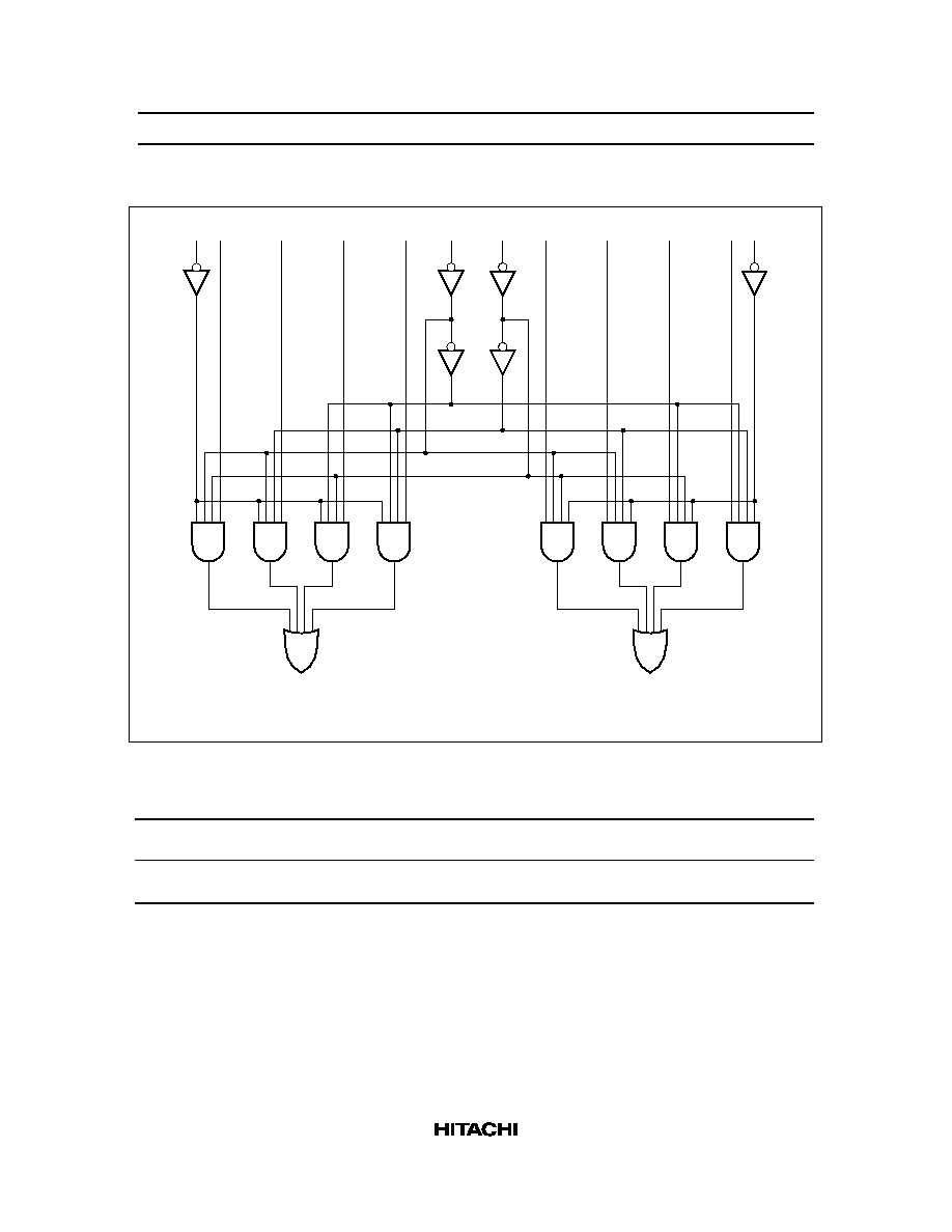
Logic Diagram
I
0a
I
1a
I
2a
I
0b
I
1b
I
2b
I
3b
E
b
E
a
I
3a
S
1
Z
a
Z
b
S
0
Please note that this diagram is provided only for the understanding of logic operations and should not be
used to estimate propagation delays.
DC Characteristics (unless otherwise specified)
Item
Symbol
Max
Unit
Condition
Maximum quiescent supply current
I
CC
80
µ
A
V
IN
= V
CC
or ground, V
CC
= 5.5 V,
Ta = Worst case
Maximum quiescent supply current
I
CC
8.0
µ
A
V
IN
= V
CC
or ground, V
CC
= 5.5 V,
Ta = 25
°
C
HD74AC153
5
AC Characteristics: HD74AC153
Ta = +25
°
C
C
L
= 50 pF
Ta = 40
°
C to +85
°
C
C
L
= 50 pF
Item
Symbol
V
CC
(V)*
1
Min
Typ
Max
Min
Max
Unit
Propagation delay
t
PLH
3.3
1.0
9.5
15.0
1.0
17.5
ns
S
n
to Z
n
5.0
1.0
6.5
11.0
1.0
12.5
Propagation delay
t
PHL
3.3
1.0
8.5
14.5
1.0
16.5
ns
S
n
to Z
n
5.0
1.0
6.5
11.0
1.0
12.0
Propagation delay
t
PLH
3.3
1.0
8.0
13.5
1.0
16.0
ns
E
n
to Z
n
5.0
1.0
5.5
9.5
1.0
11.0
Propagation delay
t
PHL
3.3
1.0
7.0
11.0
1.0
12.5
ns
E
n
to Z
n
5.0
1.0
5.0
8.0
1.0
9.0
Propagation delay
t
PLH
3.3
1.0
7.5
12.5
1.0
14.5
ns
I
n
to Z
n
5.0
1.0
5.5
9.0
1.0
10.5
Propagation delay
t
PHL
3.3
1.0
7.0
11.5
1.0
13.0
ns
I
n
to Z
n
5.0
1.0
5.0
8.5
1.0
10.0
Note:
1. Voltage Range 3.3 is 3.3 V
±
0.3 V
Voltage Range 5.0 is 5.0 V
±
0.5 V
Capacitance
Item
Symbol
Typ
Unit
Condition
Input capacitance
C
IN
4.5
pF
V
CC
= 5.5 V
Power dissipation capacitance
C
PD
65.0
pF
V
CC
= 5.0 V