 | –≠–ª–µ–∫—Ç—Ä–æ–Ω–Ω—ã–π –∫–æ–º–ø–æ–Ω–µ–Ω—Ç: HA12187FP | –°–∫–∞—á–∞—Ç—å:  PDF PDF  ZIP ZIP |

HA12187FP
Bus Interface Driver/Receiver IC
ADE-207-174A (Z)
2nd Edition
Jun. 1999
Description
The HA12187FP was developed to be used as a bus interface driver/receiver IC in automotive audio
equipment controllers. It implements a two-wire serial bus.
Functions
∑
Two-input OR circuit
∑
Input comparator circuit
∑
Current output driver circuit
∑
Receiver input comparator circuit
∑
Receiver output circuit
∑
Standby circuit
Features
∑
Supports two data inputs (Pins 1 and 3 are the input pins)
∑
Comparators with hysteresis characteristics were adopted for the inputs
∑
Current drive output drivers adopted (Output current: 3.8 mA typical)
∑
Comparators with hysteresis characteristics were adopted for the receivers
∑
Wide receiver common-mode input operating range (Common-mode input operating range: 0 to 5 V
typical)
∑
The driver output and the receiver input can withstand high voltages (Maximum rating: 18 V)
∑
Standby function (The IC enters standby mode when pin 8 goes low)
∑
Operating power-supply voltage range: 5 V ±0.5 V
HA12187FP
Rev.2, Jun. 1999, page 2 of 23
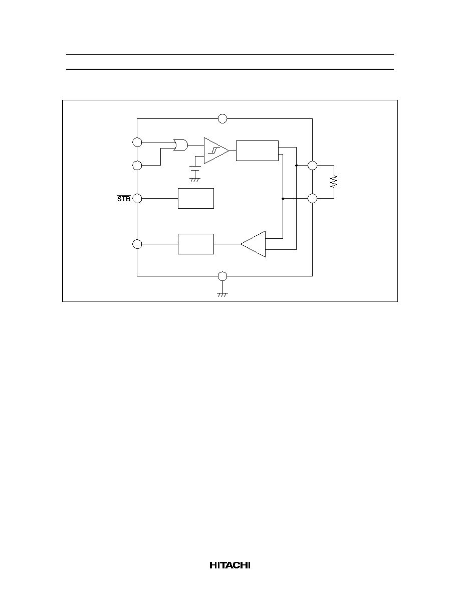
Block Diagram
+
≠
≠
+
7
1
3
S2
S1
COM
8
BIAS
Driver output
(current)
2
R
Receiver
output
4
6
5
V
CC
BUS (+)
BUS (≠)

HA12187FP
Rev.2, Jun. 1999, page 3 of 23
Pin Functions
Pin No.
Symbol
Function
Equivalent Circuit
1
S1
Data input
1
20 k
2
R out
Receiver output
2
SW
SW
100
3
S2
Data input
3
20k
4
GND
GND
5
BUS (≠)
Bus output (≠) Receiver input (≠)
6
BUS (+)
Bus output (+) Receiver input (+)
6
SW
Receiver input (+)
I
5
I
V
REF
Receiver input (≠)
7
V
CC
Power supply
8
STB
Standby control input
8
20 k
100 k

HA12187FP
Rev.2, Jun. 1999, page 4 of 23
Absolute Maximum Ratings (Ta = 25∞C)
Item
Symbol
Ratings
Unit
Notes
Power-supply voltage
V
CC
7
V
Allowable power dissipation
Pd
400
mW
Ta
85∞C
Operating temperature
Topr
≠40 to 85
∞C
Storage temperature
Tstg
≠55 to 125
∞C
Input voltage
Vin
≠1.0 to 6.7
V
Bus input voltage
Bus
18
V
Note:
Recommended operating power supply voltage range: 5 V ±0.5 V

HA12187FP
Rev.2, Jun. 1999, page 5 of 23
Electrical Characteristics (V
CC
= 5.0 V, Ta = 25∞C)
Item
Symbol
Min
Typ
Max
Unit
Test Conditions
Test
Pin
Test
Circuit
S1
High-level input
voltage
V
IHS1
3.5
--
--
V
V1 = 0 V
5 V, V3 = 0 V
With the potential
difference between pin 5
and pin 6 120 mV or more
1
Figure 1
Low-level input
voltage
V
ILS1
--
--
1.5
V
V1 = 5 V
0 V, V3 = 0 V
With the potential
difference between pin5
and pin 6 20 mV or less
1
High-level input
current
I
IHS1
--
--
1
µA
V1 = 5 V, V3 = 0 V
1
Low-level input
current
I
ILS1
--
--
1
µA
V1 = 0 V, V3 = 0 V
1
S2
High-level input
voltage
V
IHS2
3.5
--
--
V
V3 = 0 V
5 V, V1 = 0 V
With the potential
difference between pin 5
and pin 6 120 mV or more
3
Figure 1
Low-level input
voltage
V
ILS2
--
--
1.5
V
V3 = 5 V
0 V, V1 = 0 V
With the potential
difference between 5 and
pin 6 20 mV or less
3
High-level input
current
I
IHS2
--
--
1
µA
V1 = 0 V, V3 = 5 V
3
Low-level input
current
I
ILS2
--
--
1
µA
V1 = 0 V, V3 = 0 V
3
Driver High-level
output current
I
OH
3.0
3.8
4.8
mA
I
OH
= | V
OHD+
≠ V
OHD≠
| / 62
5, 6
Figure 1
Low-level output
leakage current
I
OL
--
--
1
µA
Pin 5 voltage = V
OP≠
I
OL
= | V
OP+
≠ V
OP≠
| / RI
5, 6
Reference
operating
voltage (+)
V
OP+
2.3
2.5
2.7
V
V1 = 0 V, V3 = 0 V
6
Reference
operating
voltage (≠)
V
OP≠
2.3
2.5
2.7
V
V1 = 0 V, V3 = 0 V
5
Current drain 1
I
CC
H
5.5
7.3
9.5
mA
V1 = 5 V, V3 = 0 V
7
Figure 1
Current drain 2
I
CC
L
1.7
2.2
2.7
mA
V1 = 0 V, V3 = 0 V
7
Figure 1