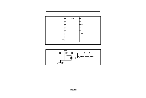
ChipFind - документация

Электронный компонент: HD74HC75

Скачать:  PDF   ZIP
www.docs.chipfind.ru
background image
HD74HC75
Quad. Bistable Latches
Description
This latch is ideally suited for use as temporary storage for binary information processing, input/output, and
indicator units. Information present at the data (D) input is transferred to the Q output when the latch
enable (LE) is high. The Q output will follow the data input as long as the enable remains high. when the
enable goes low, the information that was present at the data input at the time the transition occurred is
retained at thte Q output unit the enable is permitted to go high again.
Features
High Speed Operation: t
pd
(D to Q) = 12.5 ns typ (C
L
= 50 pF)
High Output Current: Fanout of 10 LSTTL Loads
Wide Operating Voltage: V
CC
= 2 to 6 V
Low Input Current: 1 A max
Low Quiescent Supply Current: I
CC
(static) = 2 A max (Ta = 25C)
Function Table
Inputs
Outputs
D
Latch Enable
Q
Q
L
H
L
H
H
H
H
L
X
L
Q
0
Q
0
background image
HD74HC75
2
Pin Arrangement
1
2
3
4
5
6
7
8
Q
0a
D
0a
D
1a
LE
b
V
CC
D
0b
D
1b
Q
1b
Q
0a
Q
1a
Q
1a
LE
a
GND
Q
0b
Q
0b
Q
1b
16
15
14
13
12
11
10
9
(Top view)
Block Diagram
Data
Q
Q
Latch
Enable
background image
HD74HC75
3
DC Characteristics
Ta = 25
C
Ta = 40 to
+85
C
Item
Symbol
V
CC
(V) Min Typ Max Min
Max
Unit
Test Conditions
Input voltage
V
IH
2.0
1.5
--
--
1.5
--
V
4.5
3.15 --
--
3.15
--
6.0
4.2
--
--
4.2
--
V
IL
2.0
--
--
0.5
--
0.5
V
4.5
--
--
1.35 --
1.35
6.0
--
--
1.8
--
1.8
Output voltage
V
OH
2.0
1.9
2.0
--
1.9
--
V
Vin = V
IH
or V
IL
I
OH
= 20
A
4.5
4.4
4.5
--
4.4
--
6.0
5.9
6.0
--
5.9
--
4.5
4.18 --
--
4.13
--
I
OH
= 4 mA
6.0
5.68 --
--
5.63
--
I
OH
= 5.2 mA
V
OL
2.0
--
0.0
0.1
--
0.1
V
Vin = V
IH
or V
IL
I
OL
= 20
A
4.5
--
0.0
0.1
--
0.1
6.0
--
0.0
0.1
--
0.1
4.5
--
--
0.26 --
0.33
I
OL
= 4 mA
6.0
--
--
0.26 --
0.33
I
OL
= 5.2 mA
Input current
Iin
6.0
--
--
0.1 --
1.0
A
Vin = V
CC
or GND
Quiescent supply
current
I
CC
6.0
--
--
2.0
--
20
A
Vin = V
CC
or GND, Iout = 0
A
background image
HD74HC75
4
AC Characteristics (C
L
= 50 pF, Input t
r
= t
f
= 6 ns)
Ta = 25
C
Ta = 40 to
+85
C
Item
Symbol
V
CC
(V) Min Typ Max Min
Max
Unit
Test Conditions
Propagation delay t
PLH
2.0
--
--
125 --
155
ns
D to Q
time
t
PHL
4.5
--
12
25
--
31
6.0
--
--
21
--
26
2.0
--
--
110 --
140
D to
Q
4.5
--
13
22
--
28
6.0
--
--
19
--
24
2.0
--
--
145 --
180
Latch Enable to Q
4.5
--
12
29
--
36
6.0
--
--
25
--
31
2.0
--
--
125 --
155
Latch Enable to
Q
4.5
--
13
25
--
31
6.0
--
--
21
--
26
Output rise/fall
t
TLH
2.0
--
--
75
--
95
ns
time
t
THL
4.5
--
5
15
--
19
6.0
--
--
13
--
16
Setup time
t
su
2.0
100 --
--
125
--
ns
Data to Latch Enable
4.5
20
4
--
25
--
6.0
17
--
--
21
--
Hold time
t
h
2.0
5
--
--
5
--
ns
Latch Enable to Data
4.5
5
0
--
5
--
6.0
5
--
--
5
--
Pulse width
t
w
2.0
80
--
--
100
--
ns
Latch Enable
4.5
16
5
--
20
--
6.0
14
--
--
17
--
Input capacitance
Cin
--
--
5
10
--
10
pF
background image
Hitachi Code
JEDEC
EIAJ
Weight (reference value)
DP-16
Conforms
Conforms
1.07 g
Unit: mm
6.30
19.20
16
9
8
1
1.3
20.00 Max
7.40 Max
7.62
0.25
+ 0.13
0.05
2.54
0.25
0.48
0.10
0.51 Min
2.54 Min
5.06 Max
0
15
1.11 Max