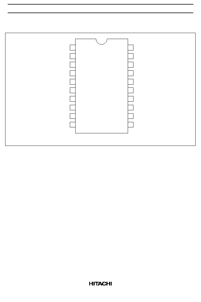
HD74LV245A
Octal Bus Transceivers with 3-state Outputs
ADE-205-247 (Z)
1st Edition
March 1999
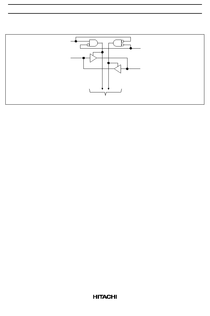
Description
The HD74LV245A has eight buffers with three-state outputs in a 20-pin package. When DIR is high, data
is transferred from the A inputs to the B outputs, and when DIR is low, data is transferred from the B inputs
to the A outputs. The A and B buses are separated by making the enable input (
OE) high level. Low-
voltage operation is suitable for battery-powered products (e.g., notebook computers), and the low power
consumption extends the battery life.
Features
∑
V
CC
= 2.0 V to 5.5 V operation
∑
All inputs V
IH
(Max.) = 5.5 V (@V
CC
= 0 V to 5.5 V)
∑
All outputs V
O
(Max.) = 5.5 V (@V
CC
= 0 V)
∑
Typical V
OL
ground bounce < 0.8 V (@V
CC
= 3.3 V, Ta = 25
∞
C)
∑
Typical V
OH
undershoot > 2.3 V (@V
CC
= 3.3 V, Ta = 25
∞
C)
∑
Output current
±
8 mA (@V
CC
= 3.0 V to 3.6 V),
±
16 mA (@V
CC
= 4.5 V to 5.5 V)
Function Table
Inputs
OE
DIR
Operation
L
L
B data to A bus
L
H
A data to B bus
H
X
Isolation
Note:
H: High level
L: Low level
X: Immaterial
HD74LV245A
3
Absolute Maximum Ratings
Item
Symbol
Ratings
Unit
Conditions
Supply voltage range
V
CC
≠0.5 to 7.0
V
Input voltage range*
1
V
I
≠0.5 to 7.0
V
Output voltage range*
1,
*
2
V
O
≠0.5 to V
CC
+ 0.5
V
Output: H or L
≠0.5 to 7.0
V
CC
: OFF or Output: Z
Input clamp current
I
IK
≠20
mA
V
I
< 0
Output clamp current
I
OK
±
50
mA
V
O
< 0 or V
O
> V
CC
Continuous output current
I
O
±
35
mA
V
O
= 0 to V
CC
Continuous current through
V
CC
or GND
I
CC
or I
GND
±
70
mA
Maximum power dissipation
at Ta = 25
∞
C (in still air)*
3
P
T
835
mW
SOP
757
TSSOP
Storage temperature
Tstg
≠65 to 150
∞
C
Notes: The absolute maximum ratings are values which must not individually be exceeded, and furthermore,
no two of which may be realized at the same time..
1. The input and output voltage ratings may be exceeded even if the input and output clamp-current
ratings are observed.
2. This value is limited to 5.5 V maximum.
3. The data above are measured by
V
BE
method mounting on glass epoxy board (40
◊
40
◊
1.6
mm) with 10% of wiring density.
HD74LV245A
4
Recommended Operating Conditions
Item
Symbol
Min
Max
Unit
Conditions
Supply voltage range
V
CC
2.0
5.5
V
Input voltage range
V
I
0
5.5
V
Output voltage range
V
O
0
V
CC
V
Output: H or L
0
5.5
High impedance state
Output current
I
OH
--
≠50
µ
A
V
CC
= 2.0 V
--
≠2
mA
V
CC
= 2.3 to 2.7 V
--
≠8
V
CC
= 3.0 to 3.6 V
--
≠16
V
CC
= 4.5 to 5.5 V
I
OL
--
50
µ
A
V
CC
= 2.0 V
--
2
mA
V
CC
= 2.3 to 2.7 V
--
8
V
CC
= 3.0 to 3.6 V
--
16
V
CC
= 4.5 to 5.5 V
Input transition rise or fall rate
t /
v
0
200
ns/V
V
CC
= 2.3 to 2.7 V
0
100
V
CC
= 3.0 to 3.6 V
0
20
V
CC
= 4.5 to 5.5 V
Operating free-air temperature
Ta
≠40
85
∞
C
Note:
Unused or floating inputs must be held high or low.