 | ÐлекÑÑоннÑй компоненÑ: HTR6545 | СкаÑаÑÑ:  PDF PDF  ZIP ZIP |
Äîêóìåíòàöèÿ è îïèñàíèÿ www.docs.chipfind.ru
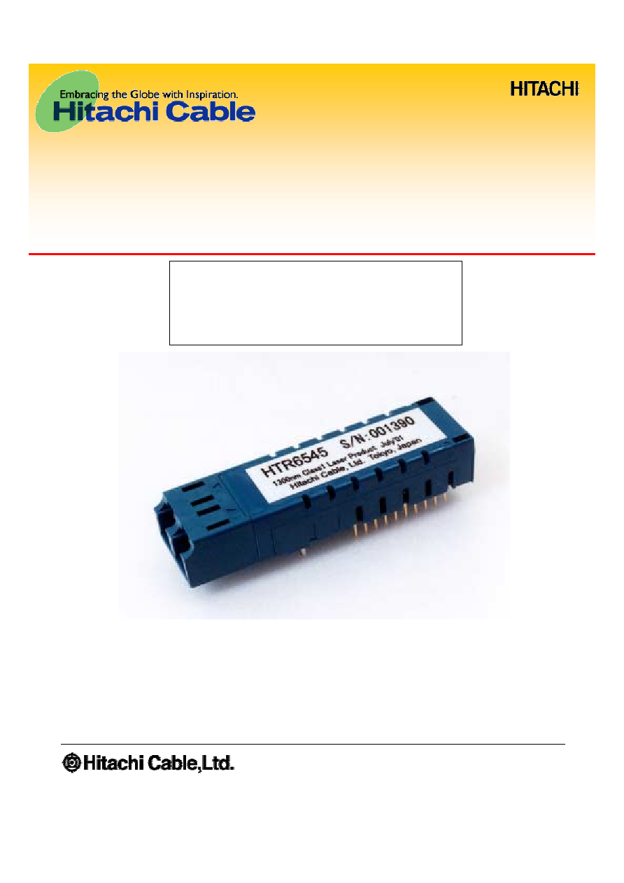
PRODUCT DATA SHEET
SFF TRANSCEIVER
for SONET/SDH
HTR6545
Series
for OC-48 SR (up to 2km)
http://www.hitachi-cable.co.jp/
Ref. No.:TE03-00-58-9039B
Mar. `03

Page 1 of 9
Features
l
SONET OC-48 SR (2.5Gbit/s, 2km) compliant.
l
Fully comply with industry standard 2x10pin Small Form Factor transceiver
with LD, PD monitor functions, without clock recovery.
l
LC duplex receptacle.
l
+3.3V single power supply.
l
Low power consumption (0.5W(typ.)).
1. General
This document specifies the characteristics of the Small Form Factor optical
transceiver (Type:HTR6545) with LC duplex receptacle for an OC-48 Short
Reach interface (SR, up to 2km).
2. Function
This transceiver is powered from a single +3.3V power supply and operated at
a data rate of 2488.32Mbps(NRZ). Optical output power is held constant by
automatic power control over the specified operating temperature and voltage
ranges. Electrical data inputs and outputs have CML logic level.
The optical output is disabled by a TTL logic level input for that purpose.
A signal Detect (SD) output is provided to indicate the presence of an incoming
optical signal. SD is a TTL compliant signal. Received optical power, laser
bias current and laser monitor current can be monitored using pins for that
purpose.
Dimensions and pin assignment fully comply with MSA (Multi Source
Agreement) for 2 by 10 type optical transceiver.
3. Absolute Maximum Ratings
Stresses in excess of the ratings listed in Table 1 can cause permanent
damage to the device and affect device reliability. Functional operation of the
device is not implied at any condition in excess of those given in the operating
specification.
Table 1. Absolute Maximum Ratings
Parameter
Symbol
Min.
Max.
Unit
Supply Voltage
V
CC
0
4.0
V
Data Input Voltage
V
IN
V
EE
V
CC
+0.3
V
Operating Ambient Temperature
T
A
0
70
deg-C
Storage Case Temperature
Tstg
-40
85
deg-C
Lead Soldering Temperature/Time
-
-
250/10
deg-C / s
Operating Relative Humidity (non-condensing
)
H
A
5
85
%

Page 2 of 9
4. Optical and Electrical Characteristics of Transmitter Portion
Optical and electrical characteristics of transmitter portion are shown in
Table 2. Unless otherwise stated, minimum and maximum values are
specified over the operating ambient temperature, and humidity ranges, DC
power supply voltage range, from beginning to end of life, using 2
23
-1 pseudo
random bit stream with a 50% duty factor.
The logic sense for the DATA input is such that a logic "1"(High) corresponds
to the maximum level of an amplitude modulated light source (Light on), while
a logic "0"(Low) corresponds to a minimum level of an amplitude modulated
light source (Light off).
Table 2. Transmitter Optical and Electrical Characteristics
Parameter
Symbol
Min
Typ
Max
Unit
Optical Output Power
Po
-10
-
-3
dBm
Center Wavelength
1266
-
1360
nm
Spectral Width(RMS)
-
-
4.0
nm
SONET Eye Mask
-
compliant with GR253 spec.
-
Extinction Ratio
-
8.2
-
-
dB
DC Power Supply Voltage
Vcc
3.135
3.3
3.465
V
DC Power Supply Current
Icc
-
-
100
mA
Data Input Voltage
Input V Range
Common Mode Input V
Diff'l Input Swing
Diff'l Input Impedance
V
IA
, V
IB
V
CI
V
ID SWING
Z
ID
V
CC
-1.2
-
300
85
-
V
CC
-0.2
-
100
V
CC
+0.2
-
1200
115
V
V
mV
p-p
ohm
Tx Disable Voltage
V
D
Vcc-1.3
-
Vcc
V
Tx Enable Voltage
V
EN
V
EE
-
V
EE
+0.8
V

Page 3 of 9
5. Optical and Electrical Characteristics of Receiver Portion
Optical and electrical characteristics of receiver portion are shown in Table 3.
Unless otherwise stated, minimum and maximum values are specified over the
operating ambient temperature, and humidity ranges, DC power supply voltage
range and wavelength range, from beginning to end of life, using a 2
23
-1 pseudo
random bit stream with a 50% duty factor.
Table 3. Receiver Optical and Electrical Characteristics
Parameter
Symbol
Min
Typ
Max
Unit
Optical input Power (Average)
a
P
IN
-18
-
-3
dBm
Signal Detect Threshold:
Decreasing Light Input
Increasing Light Input
Hysteresis
SDT
D
SDT
I
SDT
H
-28
-
0.5
-
-
-
-18
-18
6
dBm
dBm
dB
DC Power Supply Voltage
Vcc
3.135
-
3.465
V
DC Power Supply Current
Icc
-
-
80
mA
Data Output Voltage:
b
Output V
Diff'l Output Swing
Output Offset V
Diff'l Output Impedance
V
OA
, V
OB
V
OD SWING
V
CO
V
OD
V
CC
-0.5
640
-
85
-
800
V
CC
-0.2
100
V
CC
1000
-
115
V
mV
p-p
V
ohm
Output Transition Time
c
t
o
-
-
150
ps
Signal Detect Output Voltage:
d
Low
High
V
OL
V
OH
-
Vcc-0.9
-
-
0.4
-
V
V
Signal Detect Response Time:
Decreasing Light Input
Increasing Light Input
SDRT
D
SDRT
I
-
-
-
-
300
100
us
us
a. At a BER of 1x10
-10
and an extinction ratio of 8.2dB
b. CML compatible, R
L
is 50 ohm to V
CC
.
c. Between 20% and 80% (50% duty cycle)
d. TTL compatible.

Page 4 of 9
6. Physical Design
The outline for transceiver package is shown in Figure 1.
Figure 1. Package Outline
Top View
mounting studs
diameter: 1.0mm
(pin diameter)
Bottom View
1
10
11
20
0.512
13.00
0.533
13.54
0.018
0.457
0.400
10.16
0.190
4.826
0.070
1.778
0.350
8.89
0.299
7.59
max
inch
mm
unit:
Unless otherwise stated, typical values are shown
Side View
0.386
9.80
0.010
0.254
0.125
3.175
0.433
11.00
max
1.474
37.44
max
max
Page 5 of 9
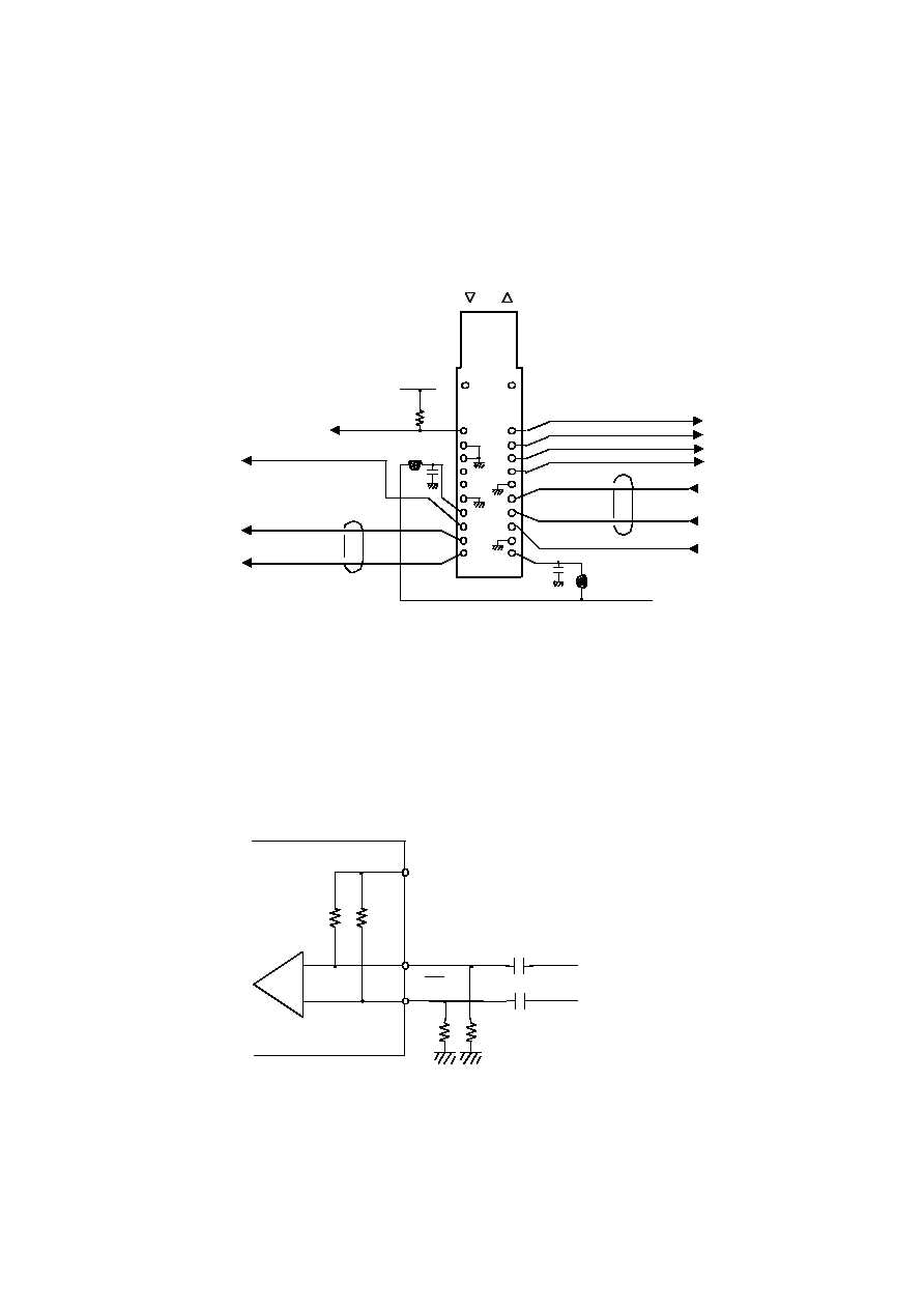
7. PINOUT
Pinout is shown in Table 4. The mounting studs are for mechanical
attachment to the circuit board and are not connected to internal circuit.
Table 4. Pin Designations
Name
Symbol
Pin
Pin
Symbol
Name
Received Power Monitor
(PD bias / APD monitor)
RMON
1
20
PMON+
LD Power Monitor(positive)
Receiver Ground
RGND
2
19
PMON-
LD Power Monitor(Negative)
Receiver Ground
RGND
3
18
BMON+
LD Bias Monitor(positive)
No Internal Connection
NC
4
17
BMON-
LD Bias Monitor(Negative)
No Internal Connection
NC
5
16
TGND
Transmitter Ground
Receiver Ground
RGND
6
15
DI
Transmit DATA(CML)
Receiver VCC(+3.3V)
RVCC
7
14
DI
Transmit DATA(CML)
Signal Detect(TTL)
SD
8
13
TD
Transmitter Disable(TTL)
Received DATA(CML)
DO
9
12
TGND
Transmitter Ground
Received DATA(CML)
DO
10
11
TVCC
Transmitter VCC(+3.3V)
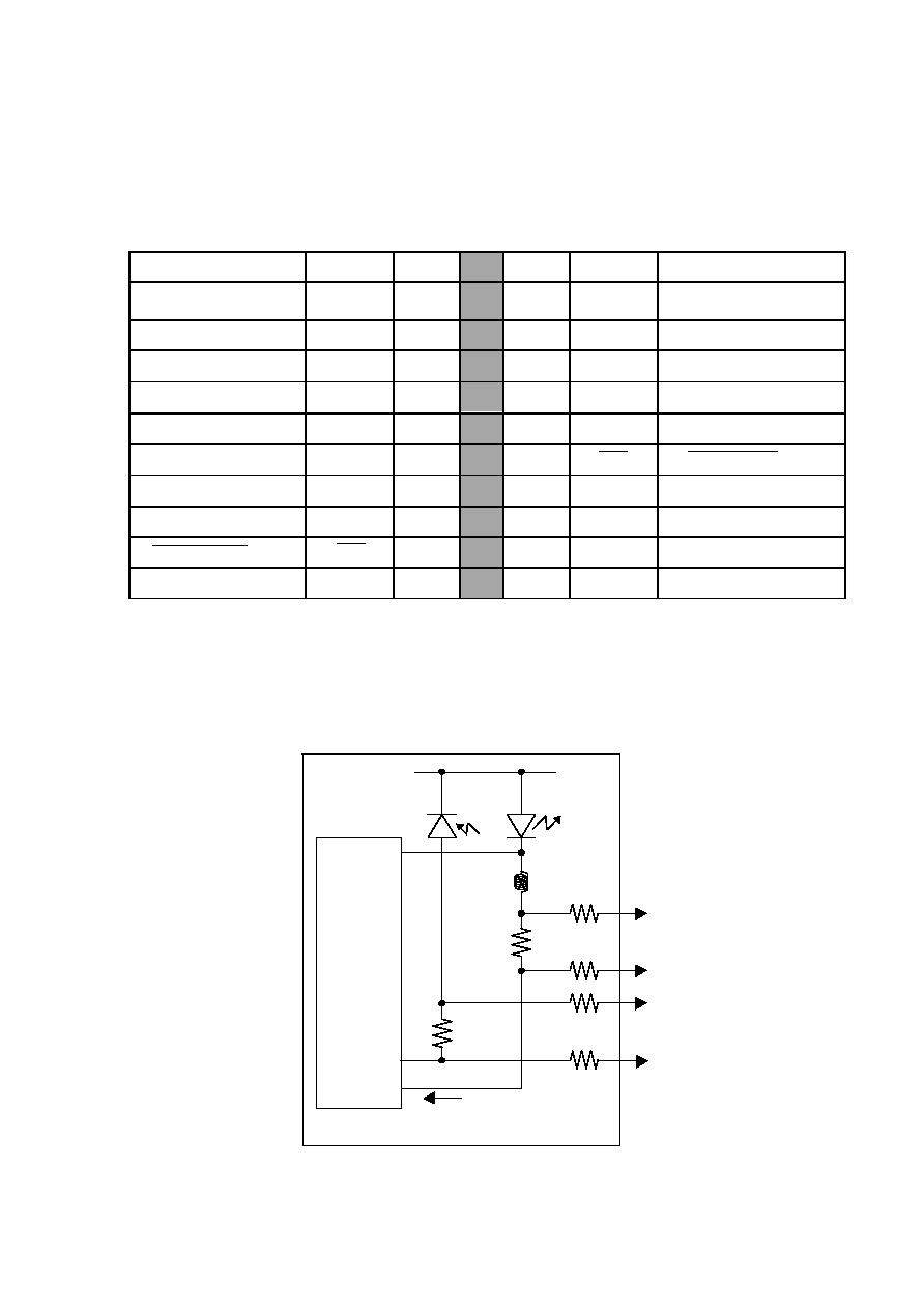
Pin 17 to Pin20 are outputs of laser monitoring function. These pins should
be connected to high impedance voltage sensing circuit. Internal circuit is
shown in Figure 2. If these function are not used, the pins should be open.
Figure 2. Equivalent internal circuit of PMON,BMON
Vcc
Monitor PD
laser
BMON+
BMON-
PMON+
PMON-
bias current
3k
3k
3k
3k
200
10
Laser
Driver
Page 6 of 9
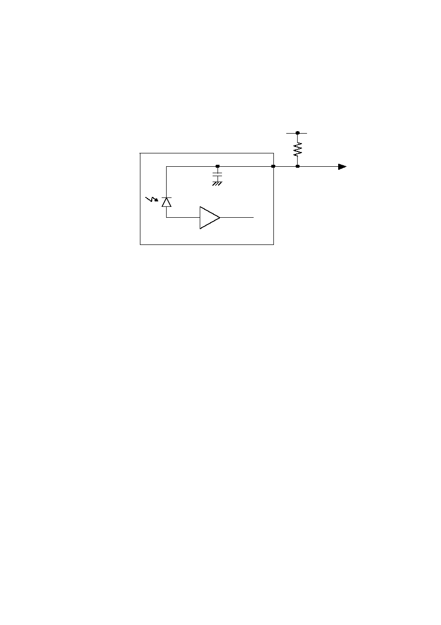
Pin 1 (RMON) could be used for received power monitoring. Equivalent
internal circuit of RMON is shown in Figure 3. RMON should be connected
to VCC Via sensing resistor: Rs (Rs is recommended less than 150ohm.).
Typical response coefficient of the PD is 0.85 A/W. If this function is not
used, connect this pin to VCC directly.
8. Inspection
Inspection items are as follows:
(1) Appearance
(2) Dimensions
(3) Optical output power
(4) Optical waveform
(5) Optical input power
a) Average Sensitivity
b) Signal Detect / Decreasing Light Input
c) Signal Detect / Increasing Light Input
(6) Power supply current
9. Packing
The optical transceiver shall be packed in sturdy carton box(es) when
shipping.
Vcc
Figure 3. Equivalent internal Circuit of RMON
Rs
RMON
PD
Preamplifier

Page 7 of 9
10. Caution
(1) Do not stare into optical output port although this product is designed to meet the
class 1 laser regulation.
(2) The housing of the transceiver is possible to crack or dissolve against the particular
chemicals. Although we recommend to use the aqueous fluid in the cleaning, the
below chemicals are checked not to affect to the housing. Pay attention in the
solder flux and cleaning process. We recommend checking the appropriateness of
the cleaning fluid in advance.
/ methyl alcohol, ethyl alcohol, butyl alcohol, isopropyl alcohol, hexane,
cyclohexane, naphtha, tetrachloroethylene, propylene glycol,
< Do not use : Chemicals which are checked to crack or dissolve>
/ trichloroethylene, trichloroethane, benzen, methyl ethyl ketone, chloroform,
toluene, acetone, phenol, ethyl acetate,
methylene di chloride, isophtalic acid dimethyl ester
(3) Optical connectors should be cleaned completely by proper cleaning process before
insertion to optical receptacles of the transceiver to avoid contamination inside the
optical receptacle.
The contamination may cause serious degradation of
transmission performance. Using forced nitrogen and some kind of cleaning stick
("CLETOP, stick type" for LC/MU connector supplied by NTT international is
recommended) should be used if the receptacle get contaminated by miss-treating
optical connectors.
Page 8 of 9
11. Recommended Circuit
Recommended decoupling and termination for HTR6545 is illustrated in
Figure 4 . This recommendation will provide a good performance of the
optical transceiver.
Figure 4. Recommended decoupling and termination
Remark : HTR6545 has input termination resistors (50 ohms to Vcc) inside
the package. If AC coupling is needed, place bias resistors outside
the package to prevent the input signal voltage from exceeding Vcc.
Vcc
DI
DI
50 ohm
500 - 750 ohm
400mV
p-p
(800mV(differential))
SD(TTL)
DOUT
(CML)
50 ohm microstrip line
10uH
1uF
1uF
DIN
(CML)
TD(TTL)
50 ohm microstrip line
10uH
VCC(+3.3V)
1
20
11
10
OPT
IN
OPT
OUT
Top View
(For received power
monitoring)
(For laser power monitoring)
VCC(filtered)

= Notice =
- All information contained in this document is subject to change without notice.
- No responsibility is assumed by Hitachi Cable, Ltd. For its use nor for any infringements
of third parties, which may result from its use.
- Products described in this document are not intended for use in implantation or other life
support applications where malfunction may result in injury or death to persons.
- Customer must contact Hitachi Cable, Ltd. to obtain the latest specification to verify,
before placing any order, that the information contained herein is current.
Ref. No.:TE03-00-58-9039B
Mar. `03
http://www.hitachi-cable.co.jp/
Hitachi Cable America, Inc.
http://www.hitachi-cable.com/
= MEMO =