 | –≠–ª–µ–∫—Ç—Ä–æ–Ω–Ω—ã–π –∫–æ–º–ø–æ–Ω–µ–Ω—Ç: MBN400C20 | –°–∫–∞—á–∞—Ç—å:  PDF PDF  ZIP ZIP |
PDE-N400C20-0
IGBT MODULE
MBN400C20
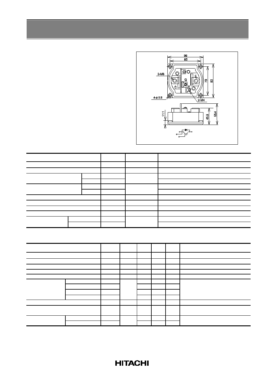
Silicon N-channel IGBT OUTLINE DRAWING
FEATURES
*
High thermal fatigue durability.
(delta Tc=70
∞
C,N
>
20,000cycles)
*
low noise due to built-in free-wheeling
diode - ultra soft fast recovery diode(USFD).
*
High speed,low loss IGBT module.
*
Low driving power due to low input
capacitance MOS gate.
*
High reliability,high durability module.
*
Isolated head sink (terminal to base).
ABSOLUTE MAXIMUM RATINGS (Tc=25
∞
C
)
Item
Symbol
Unit
MBN400C20
Collector Emitter Voltage
V
CES
V
2,000
Gate Emitter Voltage
V
GES
V
±
20
Collector Current
DC
I
C
400
1ms
I
Cp
A
800
Forward Current
DC
I
F
400
1ms
I
FM
A
800
Collector Power Dissipation
Pc
W
3,000
Junction Temperature
T
j
∞
C
-40 ~ +125
Storage Temperature
T
stg
∞
C
-40 ~ +125
Isolation Voltage
V
ISO
V
RMS
4,000(AC 1 minute)
Screw Torque
Terminals
(M4/M8)
-
2/10 (1)
Mounting
(M5)
-
N.m
2.8 (2)
Notes: (1)Recommended Value 1.8
±
0.2/9
±
1N.m (2)Recommended Value 2.6
±
0.2N.m
CHARACTERISTICS (Tc=25
∞
C
)
Item
Symbol
Unit
Min.
Typ.
Max.
Test Conditions
Collector Emitter Cut-Off Current
I
CES
mA
-
-
4.0
V
CE
=2,000V,V
GE
=0V
Gate Emitter Leakage Current
I
GES
nA
-
-
±
200 V
GE
=
±
20V,V
CE
=0V
Collector Emitter Saturation Voltage
V
CE(sat)
V
-
4.2
5.2
I
C
=400A,V
GE
=15V
Gate Emitter Threshold Voltage
V
GE(TO)
V
4.0
5.1
7.0
V
CE
=10V, I
C
=400mA
Input Capacitance
C
ies
nF
-
46
100
V
CE
=10V,V
GE
=0V,f=100KHz
Rise Time
t
r
-
1.4
2.3
V
CC
=1,000V,Ic=400A
Turn On Time
t
on
-
1.7
2.6
L=200nH
Fall Time
t
f
-
1.8
2.4
R
G
=12
W
(3)
Switching Times
Turn Off Time
t
off
m
s
-
4.0
5.9
V
GE
=
±
15V Tc=125
∞
C
Peak Forward Voltage Drop
V
FM
V
-
2.4
3.4
-
Ic=400A,V
GE
=0V
Reverse Recovery Time
t
rr
m
s
-
0.5
0.9
Vcc=1,000V,
-
Ic=400A,L=200nH,
Tc=125
∞
C (4)
IGBT
Rth(j-c)
-
-
0.033
Thermal Impedance
FWD
Rth(j-c)
∞
C/W
-
-
0.10
Junction to case
Notes:(3) R
G
value is the test condition's value for decision of the switching times, not recommended value.
Determine the suitable R
G
value after the measurement of switching waveforms
(overshoot voltage,etc.)with appliance mounted.
(4) Counter arm IGBT V
GE
=
-
15V
Weight: 350 (g)
TERMINALS
E
C
G
E
Unit in mm
1000
0
1
3
4
2
5
6
7
9
8
10
500
0
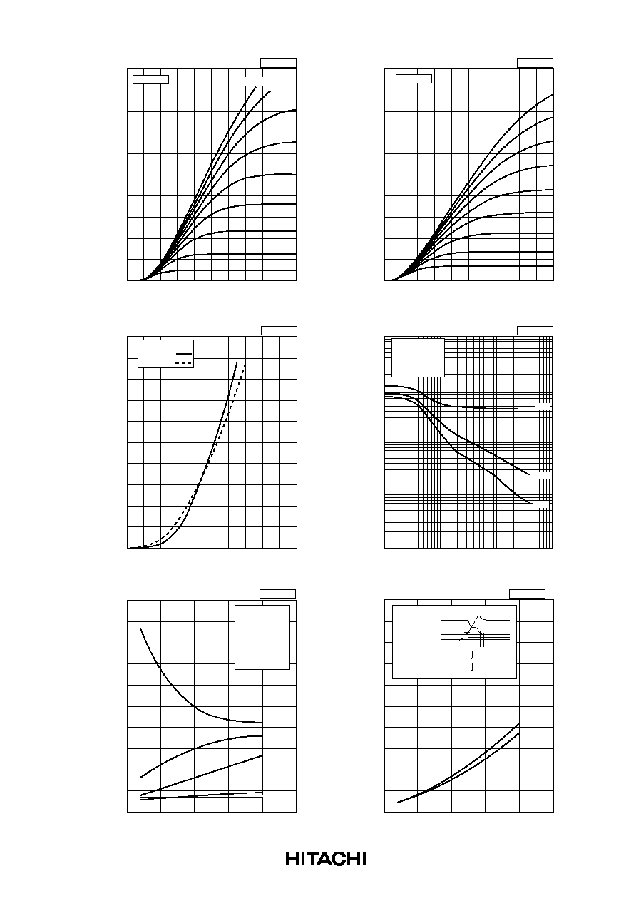
TYPICAL
Collector Current, Ic (A)
Collector Current, Ic (A)
Collector to Emitter Voltage, V
CE
(V)
Collector current vs. Collector to Emitter voltage
Switching
Time
, td(on), tr
, td(off), tf
,trr (
µ
s)
F
orw
ard Current, I
F
(A)
Collector Current, I
C
(A)
Switching time vs. Collector current
Forward Voltage, V
F
(V)
Forward voltage of free-wheeling diode
Cies
, Coes
, Cres(nF)
Collector to Emitter Voltage, V
CE
(V)
Capacitance vs. Collector to Emitter Voltage
Collector to Emitter Voltage, V
CE
(V)
Collector current vs. Collector to Emitter voltage
PDE-N400C20-0
14V
13V
tr
tf
td(off)
full
10%
trr
12V
11V
10V
9V
8V
7V
Tc
=
25
∞
C
V
GE
=
15V
1000
0
1
3
4
2
5
6
7
9
8
10
500
0
TYPICAL
7V
8V
9V
10V
11V
12V
13V
14V
V
GE
=
15V
Tc
=
125
∞
C
5
4
3
2
1
0
200
100
300
400
500
0
TYPICAL
T
u
r
n-on Loss Eon (J/pulse)
Collector Current I
C
(A)
Turn-on Loss vs. Collector Current
0.5
0.4
0.3
0.2
0.1
0
200
100
300
400
500
0
TYPICAL
1000
0
1
3
4
2
5
500
0
TYPICAL
V
GE
=
0
Tc
=
25
∞
C
Tc
=
125
∞
C
1000
100
1
10
100
10
1
0.1
0.1
TYPICAL
Cies
Coes
Cres
[Conditions]
V
GE
=
0
f
=
100KHz
Tc
=
25
∞
C
[Conditions]
Tc
=
125
∞
C
V
CC
=
1000V
Lp
200nH
RG(on)
=
12
RG(off)
=
12
V
GE
=±
15V
Inductive Load
[Conditions]
Tc
=
125
∞
C
V
CC
=
1000V
Lp
200nH
RG(on)
=
12
RG(off)
=
12
V
GE
=±
15V
Inductive Load
td(on)
t1
t1
t3
t3
t4
t4
0
10%
10%
V
GE
I
C
I
C
V
CE
dt
I
C
V
CE
dt
Eon(10%)
=
Eon(full)
=
V
CE
0
t2
t2
.
.
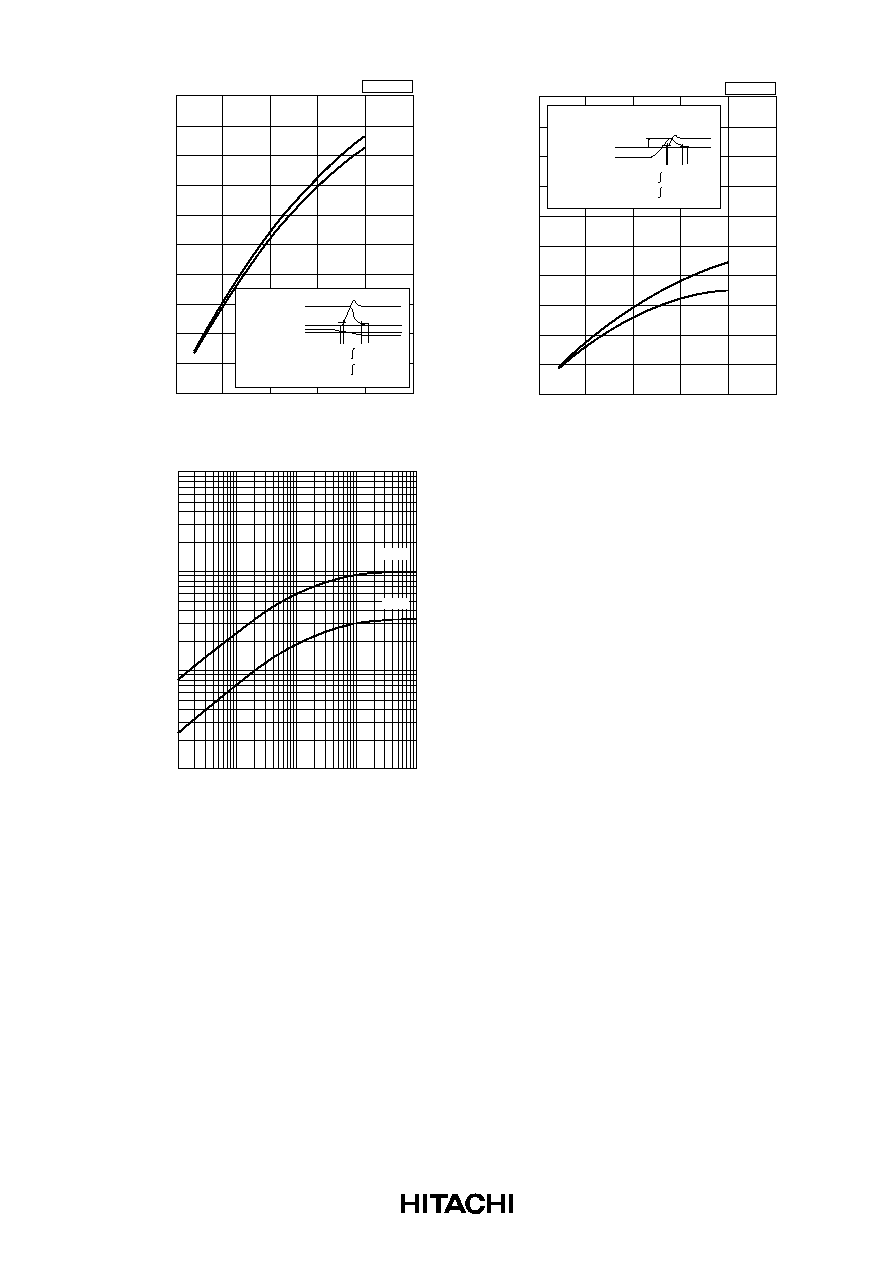
PDE-N400C20-0
full
10%
T
u
r
n-off Loss Eoff (J/pulse)
Collector Current I
C
(A)
Turn-off Loss vs. Collector Current
Reverse Recovery Loss vs. Collector Current
0.5
0.4
0.3
0.2
0.1
0
200
100
300
400
500
0
TYPICAL
0.001
0.01
1
10
0.1
0.001
0.01
0.1
1
[Conditions]
Tc
=
125
∞
C
V
CC
=
1000V
Lp
200nH
RG(on)
=
12
RG(off)
=
12
V
GE
=±
15V
Inductive Load
full
10%
Re
v
erse Reco
v
e
r
y
Loss Err (J/pulse)
Collector Current I
C
(A)
0.5
0.4
0.3
0.2
0.1
0
200
100
300
400
500
0
TYPICAL
[Conditions]
Tc
=
125
∞
C
V
CC
=
1000V
Lp
200nH
RG(on)
=
12
RG(off)
=
12
V
GE
=±
15V
Inductive Load
T
r
ansient
Ther
mal Impedance
, R
th(j-c)
(
∞
C/W
)
Time, t (s)
Transient thermal impedance
Diode
IGBT
t9
t9
t11
t11
t12
t12
10%
I
RM
0.1 I
RM
I
C
I
C
V
CE
dt
I
C
V
CE
dt
Err(10%)
=
Err(full)
=
V
CE
t
0
t10
t10
.
.
t5
t5
t7
t7
t8
t8
0
10%
10%
V
GE
I
C
I
C
V
CE
dt
I
C
V
CE
dt
Eoff(10%)
=
Eoff(full)
=
V
CE
0
t6
t
t6
.
.

1.
The information given herein, including the specifications and dimensions, is subject to
change without prior notice to improve product characteristics. Before ordering,
purchasers are adviced to contact Hitachi sales department for the latest version of this
data sheets.
2.
Please be sure to read "Precautions for Safe Use and Notices" in the individual brochure
before use.
3.
In cases where extremely high reliability is required(such as use in nuclear power control,
aerospace and aviation, traffic equipment, life-support-related medical equipment, fuel
control equipment and various kinds of safety equipment), safety should be ensured by
using semiconductor devices that feature assured safety or by means of users' fail-safe
precautions or other arrangement. Or consult Hitachi's sales department staff.
4.
In no event shall Hitachi be liable for any damages that may result from an accident or
any other cause during operation of the user's units according to this data sheets. Hitachi
assumes no responsibility for any intellectual property claims or any other problems that
may result from applications of information, products or circuits described in this data
sheets.
5.
In no event shall Hitachi be liable for any failure in a semiconductor device or any
secondary damage resulting from use at a value exceeding the absolute maximum rating.
6.
No license is granted by this data sheets under any patents or other rights of any third
party or Hitachi, Ltd.
7.
This data sheets may not be reproduced or duplicated, in any form, in whole or in part ,
without the expressed written permission of Hitachi, Ltd.
8.
The products (technologies) described in this data sheets are not to be provided to any
party whose purpose in their application will hinder maintenance of international peace
and safety not are they to be applied to that purpose by their direct purchasers or any
third party. When exporting these products (technologies), the necessary procedures are
to be taken in accordance with related laws and regulations.
HITACHI POWER SEMICONDUCTORS
For inquiries relating to the products, please contact nearest overseas representatives which is located
"Inquiry" portion on the top page of a home page.
Notices
Notices
Notices
Notices
Hitachi power semiconductor home page address http://www.hitachi.co.jp/pse