 | –≠–ª–µ–∫—Ç—Ä–æ–Ω–Ω—ã–π –∫–æ–º–ø–æ–Ω–µ–Ω—Ç: HMC322 | –°–∫–∞—á–∞—Ç—å:  PDF PDF  ZIP ZIP |

MICROWAVE CORPORATION
7 - 14
For price, delivery, and to place orders, please contact Hittite Microwave Corporation:
12 Elizabeth Drive, Chelmsford, MA 01824 Phone: 978-250-3343 Fax: 978-250-3373
Order Online at www.hittite.com
SWITCHES - CHIP
7
HMC322
GaAs MMIC SP8T NON-REFLECTIVE
SWITCH, DC - 10.0 GHz
v00.0303
General Description
Features
Functional Diagram
The HMC322 is a broadband non-refl ective
GaAs MESFET SP8T switch chip. Covering DC
to 10.0 GHz, this switch offers high isolation and
low insertion loss and extends the frequency
coverage of Hittite's SP8T switch product line.
This switch also includes an on board binary
decoder circuit which reduces the required logic
control lines to three. The switch operates using
a negative control voltage of 0/-5V, and requires
a fi xed bias of -5V. All data is tested with the chip
in a 50 Ohm test fi xture connected via 0.025 mm
(1 mil) diameter wire bonds of 0.5 mm (20 mils)
length.
Broadband Performance: DC - 10.0 GHz
High Isolation: >38 dB@ 4 GHz
Low Insertion Loss: 2.0 dB@ 4 GHz
Integrated 3:8 TTL Decoder
Small Size: 1.45 mm x 1.6 mm x 0.10 mm
Electrical Specifi cations,
T
A
= +25∞ C, With 0/-5V Control, Vee= -5V, 50 Ohm System
Typical Applications
The HMC322 is ideal for:
∑ Telecom Infrastructure
∑ Microwave Radio & VSAT
∑ Military & Space
∑ Test Instrumentation
Parameter
Frequency
Min.
Typ.
Max.
Units
Insertion Loss
DC - 2.0 GHz
DC - 4.0 GHz
DC - 6.0 GHz
DC - 8.0 GHz
DC - 10.0 GHz
1.9
2.0
2.1
2.2
2.4
2.3
2.4
2.5
2.6
2.8
dB
dB
dB
dB
dB
Isolation (RFC to RF1 - 8)
DC - 2.0 GHz
DC - 4.0 GHz
DC - 6.0 GHz
DC - 8.0 GHz
DC - 10.0 GHz
40
32
27
20
18
46
38
32
26
24
dB
dB
dB
dB
dB
Return Loss
"On State"
DC - 10.0 GHz
14
dB
Return Loss
"Off State"
DC - 10.0 GHz
11
dB
Input Power for 1 dB Compression
0.5 - 10.0 GHz
19
23
dBm
Input Third Order Intercept
(Two-Tone Input Power = +7 dBm Each Tone)
0.5 - 10.0 GHz
34
38
dBm
Switching Characteristics
tRISE, tFALL (10/90% RF)
tON, tOFF (50% CTL to 10/90% RF)
DC - 10.0 GHz
50
150
ns
ns

MICROWAVE CORPORATION
7 - 15
For price, delivery, and to place orders, please contact Hittite Microwave Corporation:
12 Elizabeth Drive, Chelmsford, MA 01824 Phone: 978-250-3343 Fax: 978-250-3373
Order Online at www.hittite.com
7
SWITCHES - CHIP
GaAs MMIC SUB-HARMONICALLY PUMPED MIXER 17 - 25 GHz
HMC322
Input Third Order Intercept Point
GaAs MMIC SP8T NON-REFLECTIVE
SWITCH, DC - 10.0 GHz
Return Loss
0.1 and 1 dB Input Compression Point
Insertion Loss vs. Temperature
Isolation Between RFC and Output Ports
v00.0303
-5
-4
-3
-2
-1
0
0
1
2
3
4
5
6
7
8
9
10
+25 C
+85 C
-55 C
INSERTION LOSS (dB)
FREQUENCY (GHz)
-70
-60
-50
-40
-30
-20
-10
0
0
1
2
3
4
5
6
7
8
9
10
RF1
RF2
RF3
RF4
RF5
RF6
RF7
RF8
ISOLATION (dB)
FREQUENCY (GHz)
-25
-20
-15
-10
-5
0
0
1
2
3
4
5
6
7
8
9
10
RFC
RF1-8 ON
RF1-8 OFF
RETURN LOSS (dB)
FREQUENCY (GHz)
25
30
35
40
45
50
1
2
3
4
5
6
7
8
9
10
+25 C
+85 C
-55 C
I
N
PUT THI
RD ORDER I
N
TERCEPT (dBm)
FREQUENCY (GHz)
18
20
22
24
26
28
1
2
3
4
5
6
7
8
9
10
1.0 Compression Point
0.1dB Compression Point
INPUT COMPRESSION POINT (dBm)
FREQUENCY (GHz)
-70
-60
-50
-40
-30
-20
-10
0
0
1
2
3
4
5
6
7
8
9
10
ISOLATION (dB)
FREQUENCY (GHz)
Isolation Between Output Ports
MICROWAVE CORPORATION
7 - 16
For price, delivery, and to place orders, please contact Hittite Microwave Corporation:
12 Elizabeth Drive, Chelmsford, MA 01824 Phone: 978-250-3343 Fax: 978-250-3373
Order Online at www.hittite.com
SWITCHES - CHIP
7
HMC322
GaAs MMIC SP8T NON-REFLECTIVE
SWITCH, DC - 10.0 GHz
v00.0303
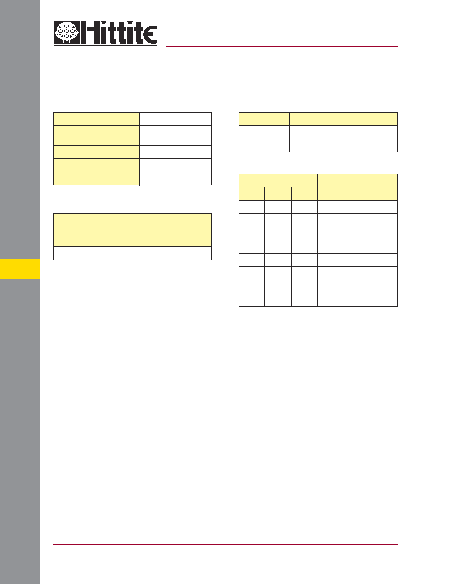
Truth Table
Bias Voltage & Current
Control Voltages
Control Input
Signal Path State
A
B
C
RFCOM to:
High
High
High
RF1
Low
High
High
RF2
High
Low
High
RF3
Low
Low
High
RF4
High
High
Low
RF5
Low
High
Low
RF6
High
Low
Low
RF7
Low
Low
Low
RF8
Vee Range = -5.0 Vdc ± 10%
Vee
(Vdc)
Iee (Typ.)
(mA)
Iee (Max.)
(mA)
-5.0
5.0
9.0
State
Bias Condition
Low
-3V to 0 Vdc @ 25 uA Typical
High
-5 to -4.2 Vdc @ 5 uA Typical
Absolute Maximum Ratings
Bias Voltage Range (Vee)
-7.0 Vdc
Control Voltage Range
(A, B, & C)
Vee -0.5V to +1.0 Vdc
Storage Temperature
-65 to +150 ∞C
Operating Temperature
-40 to +85 ∞C
RF Input Power, 0.5 - 10 GHz
+26 dBm

MICROWAVE CORPORATION
7 - 17
For price, delivery, and to place orders, please contact Hittite Microwave Corporation:
12 Elizabeth Drive, Chelmsford, MA 01824 Phone: 978-250-3343 Fax: 978-250-3373
Order Online at www.hittite.com
7
SWITCHES - CHIP
HMC322
GaAs MMIC SP8T NON-REFLECTIVE
SWITCH, DC - 10.0 GHz
v00.0303
Outline Drawing
NOTES:
1. DIMENSIONS IN INCHES [MILLIMETERS].
2. DIE
THICKNESS IS 0.004".
3. TYPICAL BOND PAD IS 0.004" SQUARE.
4. TYPICAL BOND PAD SPACING IS 0.006" CENTER TO CENTER.
5. BOND PAD METALLIZATION: GOLD.
6. BACKSIDE METALLIZATION: GOLD.
7. BACKSIDE METAL IS GROUND.
8. NO CONNECTION REQUIRED FOR UNLABELED GROUND BOND PADS.

MICROWAVE CORPORATION
7 - 18
For price, delivery, and to place orders, please contact Hittite Microwave Corporation:
12 Elizabeth Drive, Chelmsford, MA 01824 Phone: 978-250-3343 Fax: 978-250-3373
Order Online at www.hittite.com
SWITCHES - CHIP
7
Pad Number
Function
Description
Interface Schematic
1 - 7,
12 - 14
RF1, RFC,
RF8 - RF2
These pads are DC coupled and matched to 50 Ohms. Blocking
capacitors are required if RF line potential is not equal to 0V.
8
A
See truth table and control voltage table.
9
B
See truth table and control voltage table.
10
C
See truth table and control voltage table.
11
Vee
Supply Voltage = -5Vdc ± 10%
Die Bottom
GND
Die bottom must be connected to RF / DC ground.
HMC322
GaAs MMIC SP8T NON-REFLECTIVE
SWITCH, DC - 10.0 GHz
v00.0303
TTL Interface Circuit
(Required for Each Control Input A, B and C)
Note:
Control inputs A, B, and C can be driven directly with TTL logic with -5 Volts applied to the HCT logic gates Vee pin and
to the Vee pad of the RF Switch.
Pad Descriptions