Äîêóìåíòàöèÿ è îïèñàíèÿ www.docs.chipfind.ru
MICROWAVE CORPORATION
14 - 224
For price, delivery, and to place orders, please contact Hittite Microwave Corporation:
12 Elizabeth Drive, Chelmsford, MA 01824 Phone: 978-250-3343 Fax: 978-250-3373
Order Online at www.hittite.com
SWITCHES - SMT
14
HMC349LP4C
HIGH ISOLATION SPDT
NON-REFLECTIVE SWITCH, DC - 4.0 GHz
v00.0304
General Description
Features
Functional Diagram
High Isolation: 67 dB @ 1 GHz
62 dB @ 2 GHz
Single Positive Control: 0/+5V
+52 dBm Input IP3
Non-Refl ective Design
All Off State
16 mm
2
Leadless QFN SMT Package
Typical Applications
The HMC349LP4C is ideal for:
· Basestation Infrastructure
· MMDS & 3.5 GHz WLL
· CATV/CMTS
· Test Instrumentation
The HMC349LP4C is a high isolation non-
refl ective DC to 4 GHz GaAs MESFET SPDT
switch in a low cost leadless surface mount
package. The switch is ideal for cellular/PCS/3G
basestation applications yielding 60 to 65 dB
isolation, low 0.9 dB insertion loss and +52 dBm
input IP3. Power handling is excellent up through
the 3.5 GHz WLL band with the switch offering a
P1dB compression point of +31 dBm. On-chip
circuitry allows a single positive voltage control
of 0/+5 Volts at very low DC currents. An enable
input (EN) set to logic high will put the switch in
an "all off" state.
Electrical Specifi cations,
T
A
= +25° C, Vctl = 0/+5 Vdc, Vdd = +5 Vdc, 50 Ohm System
Parameter
Frequency
Min.
Typ.
Max.
Units
Insertion Loss
DC - 1.0 GHz
DC - 2.0 GHz
DC - 3.0 GHz
DC - 4.0 GHz
0.9
1.0
1.2
1.4
1.2
1.3
1.5
1.7
dB
dB
dB
dB
Isolation (RFC to RF1/RF2)
DC - 1.0 GHz
DC - 4.0 GHz
60
55
67
62
dB
dB
Return Loss (On State)
DC - 2.0 GHz
DC - 3.0 GHz
DC - 4.0 GHz
20
15
13
dB
dB
dB
Return Loss (Off State)
0.5 - 4.0 GHz
15
dB
Input Power for 1 dB Compression
0.25 - 4.0 GHz
27
31
dBm
Input Third Order Intercept
(Two-Tone Input Power = +7 dBm Each Tone)
0.25 - 1.0 GHz
1.0 - 2.0 GHz
2.0 - 3.0 GHz
3.0 - 4.0 GHz
52
50
49
46
dBm
dBm
dBm
dBm
Switching Speed
DC - 4.0 GHz
tRISE, tFALL (10/90% RF)
tON, tOFF (50% CTL to 10/90% RF)
50
120
ns
ns
MICROWAVE CORPORATION
14 - 225
For price, delivery, and to place orders, please contact Hittite Microwave Corporation:
12 Elizabeth Drive, Chelmsford, MA 01824 Phone: 978-250-3343 Fax: 978-250-3373
Order Online at www.hittite.com
14
SWITCHES - SMT
GaAs MMIC SUB-HARMONICALLY PUMPED MIXER 17 - 25 GHz
HMC349LP4C
HIGH ISOLATION SPDT
NON-REFLECTIVE SWITCH, DC - 4.0 GHz
v00.0304
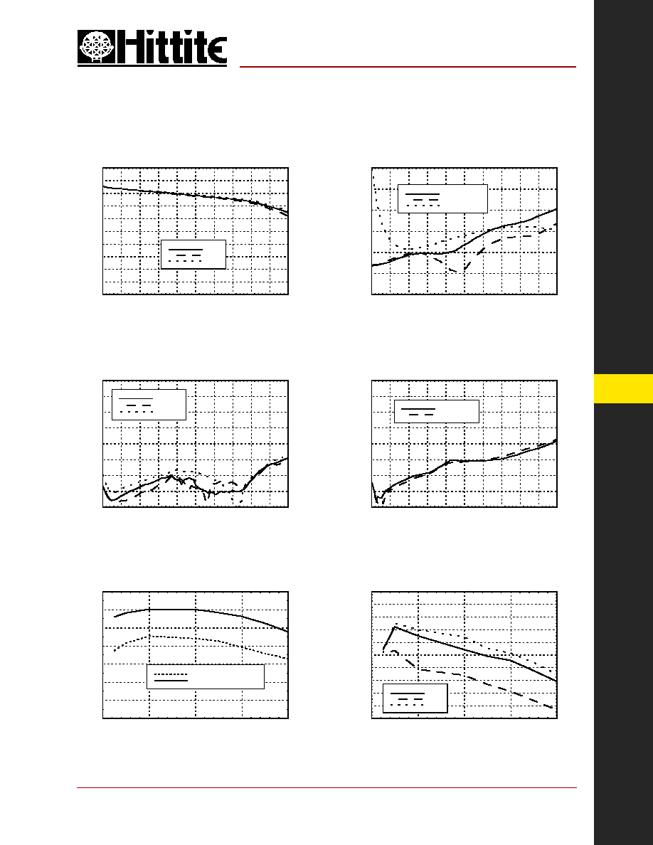
Return Loss
Insertion Loss
Isolation Between
Ports RFC and RF1 / RF2
0.1 and 1 dB Input Compression Point
Isolation Between Ports RF1 and RF2
-5
-4
-3
-2
-1
0
0
0.5
1
1.5
2
2.5
3
3.5
4
4.5
5
+25C
+85C
-40C
INSERTION LOSS (dB)
FREQUENCY (GHz)
-80
-70
-60
-50
-40
-30
-20
-10
0
0
0.5
1
1.5
2
2.5
3
3.5
4
4.5
5
RF1
RF2
ALL OFF
ISOLATION (dB)
FREQUENCY (GHz)
-80
-70
-60
-50
-40
-30
-20
-10
0
0
0.5
1
1.5
2
2.5
3
3.5
4
4.5
5
RFC-RF1 ON
RFC-RF2 ON
ISOLATION (dB)
FREQUENCY (GHz)
20
22
24
26
28
30
32
34
0
1
2
3
4
0.1 dB Compression Point
1 dB Compression Point
INPUT COMPRESSION (dBm)
FREQUENCY (GHz)
-30
-25
-20
-15
-10
-5
0
0
0.5
1
1.5
2
2.5
3
3.5
4
4.5
5
RFC
RF1, RF2 ON
RF1, RF2 OFF
RETURN LOSS (dB)
FREQUENCY (GHz)
Input Third Order Intercept Point
40
42
44
46
48
50
52
54
56
58
60
0
1
2
3
4
+25C
+85C
-40C
IIP3 (dBm)
FREQUENCY (GHz)
Note: RFC is refl ective in "all off" state.
MICROWAVE CORPORATION
14 - 226
For price, delivery, and to place orders, please contact Hittite Microwave Corporation:
12 Elizabeth Drive, Chelmsford, MA 01824 Phone: 978-250-3343 Fax: 978-250-3373
Order Online at www.hittite.com
SWITCHES - SMT
14
HMC349LP4C
HIGH ISOLATION SPDT
NON-REFLECTIVE SWITCH, DC - 4.0 GHz
v00.0304
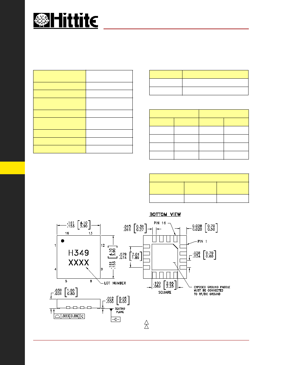
Truth Table
Absolute Maximum Ratings
NOTES:
1. PACKAGE BODY MATERIAL: LOW STRESS INJECTION MOLDED
PLASTIC SILICA AND SILICON IMPREGNATED.
2. LEADFRAME MATERIAL: COPPER ALLOY
3. LEADFRAME PLATING: Sn/Pb SOLDER
4. DIMENSIONS ARE IN INCHES [MILLIMETERS].
5. DIMENSION DOES NOT INCLUDE MOLDFLASH OF 0.15mm PER SIDE.
6. DIMENSION DOES NOT INCLUDE MOLDFLASH OF 0.25mm PER SIDE.
7. ALL GROUND LEADS AND GROUND PADDLE MUST BE SOLDERED
TO PCB RF GROUND.
Control Input
Signal Path State
Vctl
EN
RFC - RF1
RFC - RF2
Low
Low
OFF
ON
High
Low
ON
OFF
Low
High
OFF
OFF
High
High
OFF
OFF
Outline Drawing
TTL/CMOS Control Voltages
State
Bias Condition
Low
0 to +0.8 Vdc @ <1 µA Typical
High
+2.0 to +5.0 Vdc @ 30 µA Typical
RF Input Power (Vctl = 0V/+5V)
(0.25 - 4 GHz)
+30 dBm (T = +85 °C)
Supply Voltage Range (Vdd)
+7 Vdc
Control Voltage Range (Vctl)
-1V to Vdd +1V
Hot Switch Power Level
(Vdd = +5V)
+30 dBm
Channel Temperature
150 °C
Continuous Pdiss (T = 85 °C)
(derate 12 mW/°C above 85 °C)
0.75 W
Thermal Resistance
87 °C/W
Storage Temperature
-65 to +150 °C
Operating Temperature
-40 to +85 °C
Note: DC blocking capacitors are required at ports RFC,
RF1 and RF2. Their value will determine the lowest trans-
mission frequency.
Vdd Range = +5.0 Vdc ± 10%
Vdd
(Vdc)
Idd (Typ.)
(mA)
Idd (Max.)
(mA)
+5.0
2.3
5.0
Bias Voltage & Current
MICROWAVE CORPORATION
14 - 227
For price, delivery, and to place orders, please contact Hittite Microwave Corporation:
12 Elizabeth Drive, Chelmsford, MA 01824 Phone: 978-250-3343 Fax: 978-250-3373
Order Online at www.hittite.com
14
SWITCHES - SMT
HMC349LP4C
HIGH ISOLATION SPDT
NON-REFLECTIVE SWITCH, DC - 4.0 GHz
v00.0304
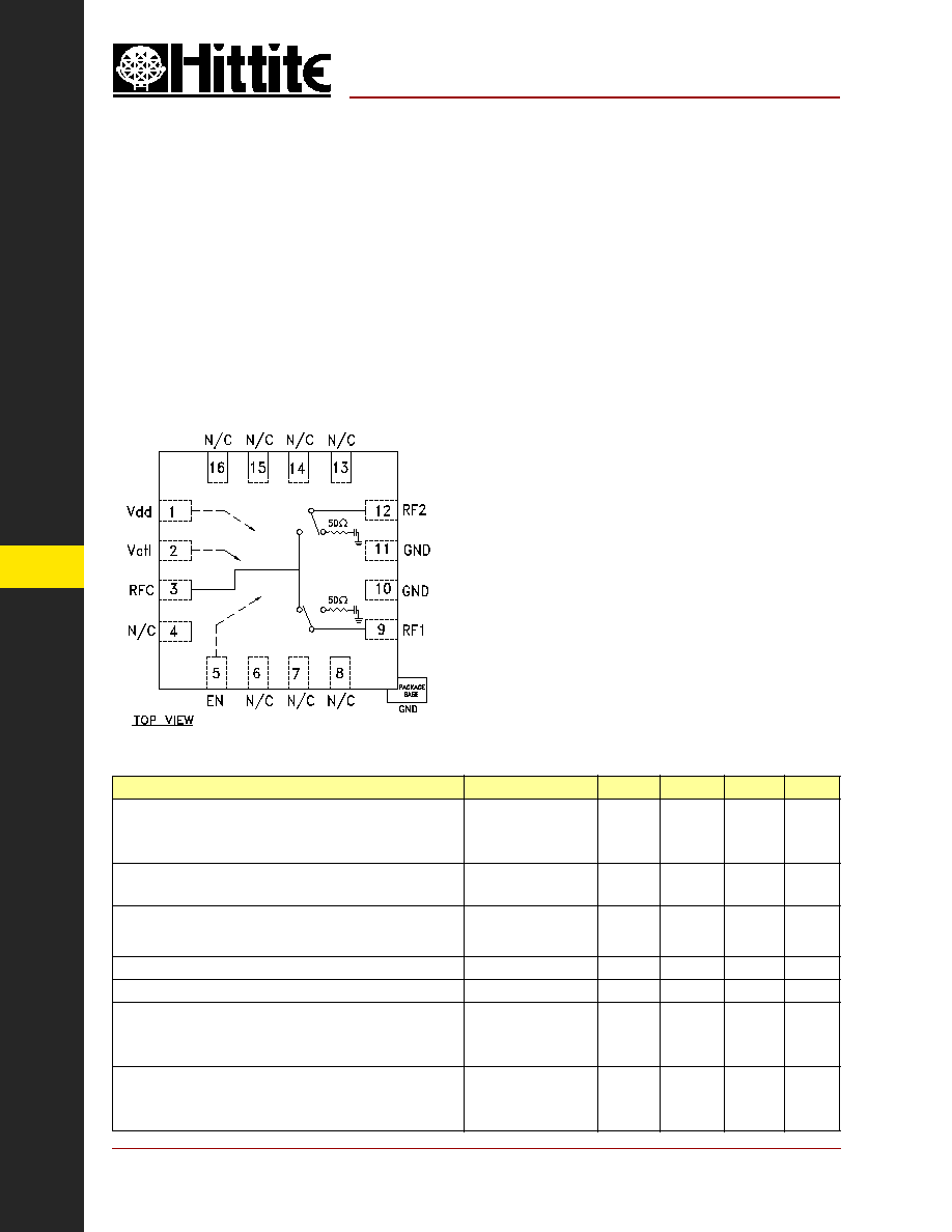
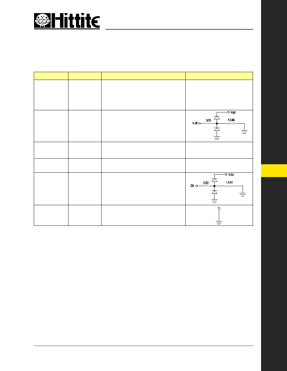
Pin Descriptions
Pin Number
Function
Description
Interface Schematic
1
Vdd
Supply Voltage.
2
Vctl
Control input. See truth and control voltage tables.
3, 9, 12
RFC, RF1, RF2
These pins are DC coupled and matched to 50 Ohms.
Blocking capacitors are required.
4, 6, 7, 8, 13, 14,
15, 16
N/C
No connection. These pins may be connected to RF
ground. Performance will not be affected.
5
EN
Enable. See truth and control voltage tables.
10, 11
GND
Package bottom must also be connected to
PCB RF ground.
MICROWAVE CORPORATION
14 - 228
For price, delivery, and to place orders, please contact Hittite Microwave Corporation:
12 Elizabeth Drive, Chelmsford, MA 01824 Phone: 978-250-3343 Fax: 978-250-3373
Order Online at www.hittite.com
SWITCHES - SMT
14
HMC349LP4C
HIGH ISOLATION SPDT
NON-REFLECTIVE SWITCH, DC - 4.0 GHz
v00.0304
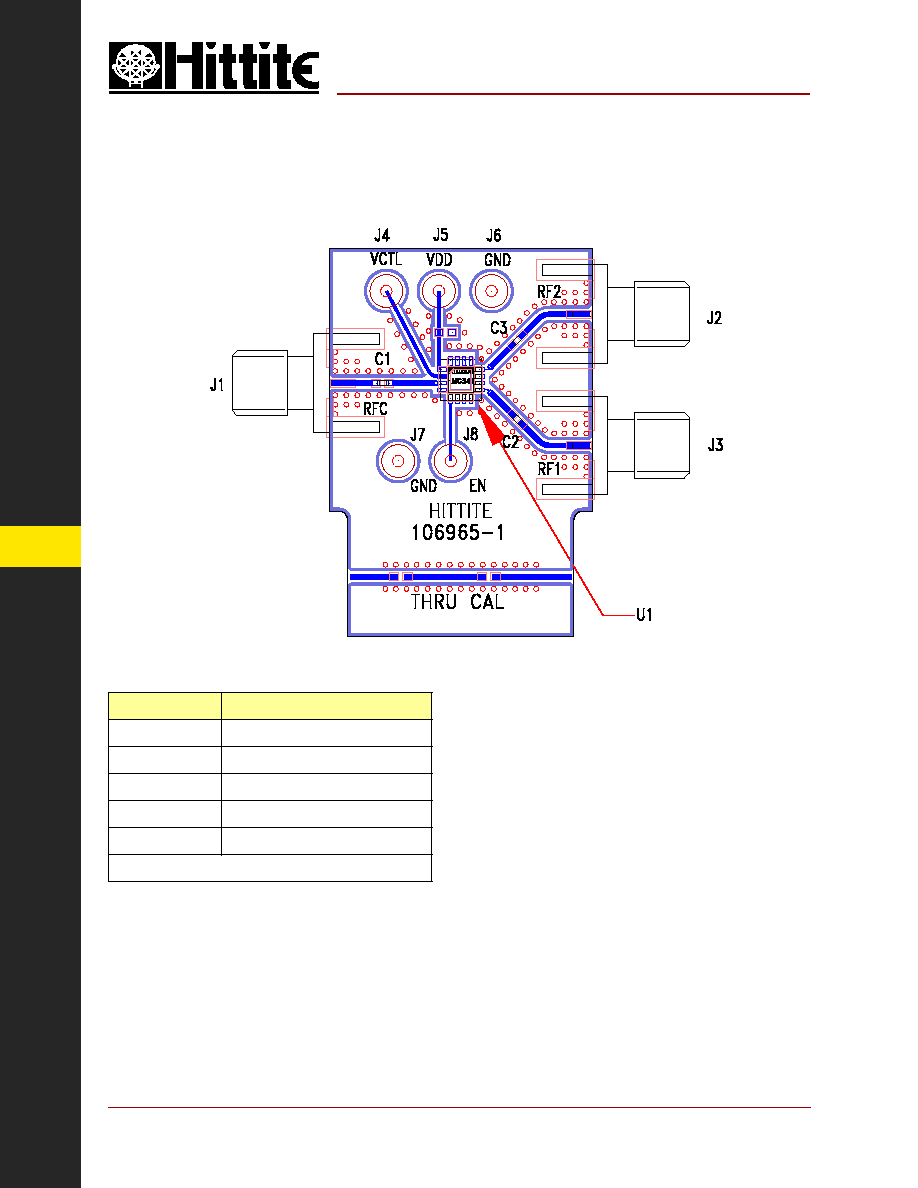
Evaluation PCB
The circuit board used in the fi nal application should
be generated with proper RF circuit design techniques.
Signal lines at the RF port should have 50 ohm imped-
ance and the package ground leads and backside
ground slug should be connected directly to the ground
plane similar to that shown above. The evaluation circuit
board shown above is available from Hittite Microwave
Corporation upon request.
List of Material for Evaluation PCB 106975*
Item
Description
J1 - J3
PC Mount SMA RF Connector
J4 - J8
DC Pin
C1 - C3
100 pF Capacitor, 0402 Pkg.
U1
HMC349LP4C SPDT Switch
PCB**
106965 Evaluation PCB
** Circuit Board Material: Rogers 4350
* Reference this number when ordering complete evaluation PCB.