8
A
M
P
L
IF
IE
RS
-
S
M
T
8 - 144
For price, delivery, and to place orders, please contact Hittite Microwave Corporation:
20 Alpha Road, Chelmsford, MA 01824 Phone: 978-250-3343 Fax: 978-250-3373
Order On-line at www.hittite.com
HMC382LP3
/
382LP3E
GaAs PHEMT MMIC
LOW NOISE AMPLIFIER, 1.7 - 2.2 GHz
v00.1005
General Description
Features
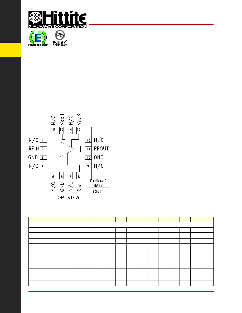
Functional Diagram
The HMC382LP3 & HMC382LP3E high dynamic
range GaAs PHEMT MMIC Low Noise Amplifi ers are
ideal for GSM & CDMA cellular basestation front-end
receivers operating between 1.7 and 2.2 GHz. This
LNA has been optimized to provide 1.0 dB noise fi gure,
17 dB gain and +30 dBm output IP3 from a single
supply of +5.0V. Input and output return losses are
13 dB typical and the LNA requires no external mat-
ching components. The HMC382LP3 & HMC382LP3E
share the same package and pinout with the
HMC376LP3 0.7 - 1.0 GHz LNA. The HMC382LP3 &
HMC382LP3E feature an externally adjustable supply
current which allows the designer to tailor the linearity
performance of the LNA for each application.
Noise Figure: 1.0 dB
Output IP3: +30 dBm
Gain: 17 dB
Externally Adjustable Supply Current
Single Positive Supply: +5.0V
50 Ohm Matched Input/Output
Electrical Specifications,
T
A
= +25� C, Vdd1, Vdd2 = +5V, Rbias = 16 Ohms*
Typical Applications
The HMC382LP3 / HMC382LP3E is ideal for:
� Cellular/3G Infrastructure
� Base Stations & Repeaters
� CDMA, W-CDMA, & TD-SCDMA
� GSM/GPRS & EDGE
Parameter
Min.
Typ.
Max.
Min.
Typ.
Max.
Min.
Typ.
Max.
Min.
Typ.
Max.
Units
Frequency Range
1.7 - 1.9
1.9 - 2.0
2.0 - 2.1
2.1 - 2.2
GHz
Gain
14
17
12
15
11
14
9
12
dB
Gain Variation Over Temperature
0.01
0.015
0.01
0.015
0.01
0.015
0.01
0.015
dB/�C
Noise Figure
1.0
1.3
1.05
1.35
1.15
1.45
1.2
1.5
dB
Input Return Loss
13
12
11
10
dB
Output Return Loss
10
13
12
9
dB
Reverse Isolation
37
36
35
35
dB
Output Power for
1dB Compression (P1dB)
16
16
15.5
14
dBm
Output Third Order Intercept (IP3)
(-20 dBm Input Power per tone,
1 MHz tone spacing)
29.5
30
30
29.5
dBm
Supply Current (Idd1 + Idd2)
67
67
67
67
mA
* Rbias resistor value sets current. See application circuit herein.
8
A
M
P
L
IF
IE
RS
-
S
M
T
8 - 145
For price, delivery, and to place orders, please contact Hittite Microwave Corporation:
20 Alpha Road, Chelmsford, MA 01824 Phone: 978-250-3343 Fax: 978-250-3373
Order On-line at www.hittite.com
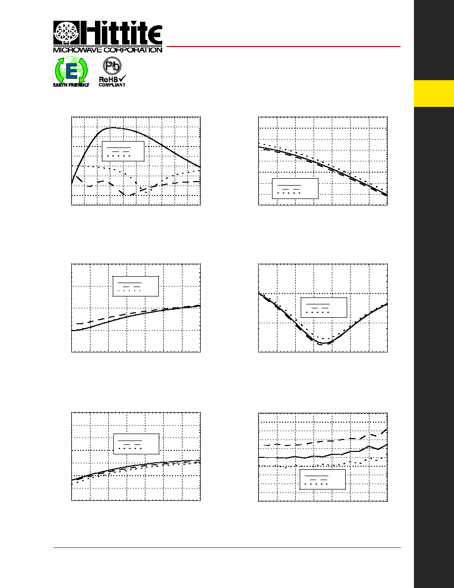
Broadband Gain & Return Loss
Input Return Loss vs. Temperature
Noise Figure vs. Temperature
Gain vs. Temperature
-20
-15
-10
-5
0
5
10
15
20
25
0.5
0.75
1
1.25
1.5
1.75
2
2.25
2.5
2.75
3
S21
S11
S22
RESPONSE (dB)
FREQUENCY (GHz)
HMC382LP3
/
382LP3E
v00.1005
Reverse Isolation vs. Temperature
Output Return Loss vs. Temperature
-15
-10
-5
0
1.6
1.7
1.8
1.9
2
2.1
2.2
2.3
+25 C
+85 C
-40 C
RETURN LOSS (dB)
FREQUENCY (GHz)
-50
-45
-40
-35
-30
-25
-20
-15
1.6
1.7
1.8
1.9
2
2.1
2.2
2.3
+25 C
+85 C
-40 C
ISOLATION (dB)
FREQUENCY (GHz)
0
0.2
0.4
0.6
0.8
1
1.2
1.4
1.6
1.8
2
1.6
1.7
1.8
1.9
2
2.1
2.2
2.3
+25 C
+85 C
-40 C
NOI
SE FI
GURE (dB)
FREQUENCY (GHz)
-20
-15
-10
-5
0
1.6
1.7
1.8
1.9
2
2.1
2.2
2.3
+25 C
+85 C
-40 C
RETURN LOSS (dB)
FREQUENCY (GHz)
8
10
12
14
16
18
20
22
24
1.6
1.7
1.8
1.9
2
2.1
2.2
2.3
+25 C
+85 C
-40 C
GAIN
(dB)
FREQUENCY (GHz)
GaAs PHEMT MMIC
LOW NOISE AMPLIFIER, 1.7 - 2.2 GHz
8
A
M
P
L
IF
IE
RS
-
S
M
T
8 - 146
For price, delivery, and to place orders, please contact Hittite Microwave Corporation:
20 Alpha Road, Chelmsford, MA 01824 Phone: 978-250-3343 Fax: 978-250-3373
Order On-line at www.hittite.com
Typical Supply Current vs. Vdd1 & Vdd2
Vdd (Vdc)
Idd (mA)
+4.5
67.2
+5.0
67.4
+5.5
67.6
Drain Bias Voltage (Vdd1, Vdd2)
+8.0 Vdc
RF Input Power (RFin)(Vs = +5.0 Vdc)
+10 dBm
Channel Temperature
150 �C
Continuous Pdiss (T = 85 �C)
(derate 6.94 mW/�C above 85 �C)
0.451 W
Thermal Resistance
(channel to ground paddle)
144 �C/W
Storage Temperature
-65 to +150 �C
Operating Temperature
-40 to +85 �C
Absolute Maximum Ratings
ELECTROSTATIC SENSITIVE DEVICE
OBSERVE HANDLING PRECAUTIONS
HMC382LP3
/
382LP3E
v00.1005
Recommended Bias Resistor Values
for Various Idd1 & Idd2
Idd1 + Idd2 (mA)
Rbias (Ohms)
60
27
70
16
80
13
100
8.2
120
3.9
GaAs PHEMT MMIC
LOW NOISE AMPLIFIER, 1.7 - 2.2 GHz
Gain, Noise Figure & P1dB vs.
Supply Current @ 1900 MHz
12
14
16
18
20
22
24
0.2
0.4
0.6
0.8
1
1.2
1.4
60
70
80
90
100
110
120
GAIN
P1dB
Noise figure
GAIN (dB) & P1dB (dBm)
NOISE FIGURE (dB)
SUPPLY CURRENT (mA)
P1dB vs. Temperature @ Idd = 67 mA
Output IP3 vs. Temperature Idd = @ 67 mA
Psat vs. Temperature @ Idd = 67 mA
10
11
12
13
14
15
16
17
18
19
20
1.7
1.8
1.9
2
2.1
2.2
+25 C
+85 C
-40 C
P1dB (dBm)
FREQUENCY (GHz)
20
21
22
23
24
25
26
27
28
29
30
31
32
33
34
1.7
1.8
1.9
2
2.1
2.2
+25 C
+85 C
-40 C
OUTPUT IP3 (dBm)
FREQUENCY (GHz)
10
11
12
13
14
15
16
17
18
19
20
1.7
1.8
1.9
2
2.1
2.2
+25 C
+85 C
-40 C
Psat (dBm)
FREQUENCY (GHz)
8
A
M
P
L
IF
IE
RS
-
S
M
T
8 - 147
For price, delivery, and to place orders, please contact Hittite Microwave Corporation:
20 Alpha Road, Chelmsford, MA 01824 Phone: 978-250-3343 Fax: 978-250-3373
Order On-line at www.hittite.com
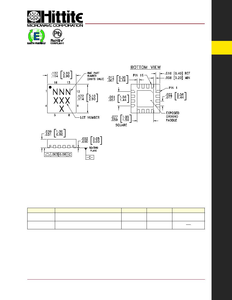
Outline Drawing
NOTES:
1. LEADFRAME MATERIAL: COPPER ALLOY
2. DIMENSIONS ARE IN INCHES [MILLIMETERS]
3. LEAD SPACING TOLERANCE IS NON-CUMULATIVE
4. PAD BURR LENGTH SHALL BE 0.15mm MAXIMUM.
PAD BURR HEIGHT SHALL BE 0.05mm MAXIMUM.
5. PACKAGE WARP SHALL NOT EXCEED 0.05mm.
6. ALL GROUND LEADS AND GROUND PADDLE MUST
BE SOLDERED TO PCB RF GROUND.
7. REFER TO HITTITE APPLICATION NOTE FOR SUGGESTED
LAND PATTERN.
Part Number
Package Body Material
Lead Finish
MSL Rating
Package Marking
[3]
HMC382LP3
Low Stress Injection Molded Plastic
Sn/Pb Solder
MSL1
[1]
382
XXXX
HMC382LP3E
RoHS-compliant Low Stress Injection Molded Plastic
100% matte Sn
MSL1
[2]
382
XXXX
[1] Max peak refl ow temperature of 235 �C
[2] Max peak refl ow temperature of 260 �C
[3] 4-Digit lot number XXXX
Package Information
HMC382LP3
/
382LP3E
v00.1005
GaAs PHEMT MMIC
LOW NOISE AMPLIFIER, 1.7 - 2.2 GHz
8
A
M
P
L
IF
IE
RS
-
S
M
T
8 - 148
For price, delivery, and to place orders, please contact Hittite Microwave Corporation:
20 Alpha Road, Chelmsford, MA 01824 Phone: 978-250-3343 Fax: 978-250-3373
Order On-line at www.hittite.com
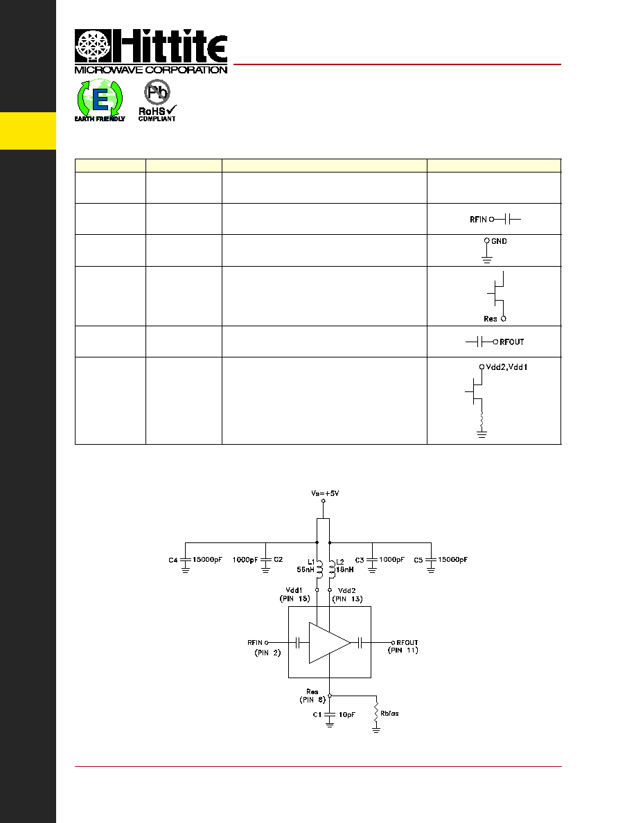
Pin Number
Function
Description
Interface Schematic
1, 4, 5, 7, 9,
12, 14, 16
N/C
No connection necessary. These pins may be connected to
RF/DC ground. Performance will not be affected.
2
RFIN
This pin is AC coupled and matched to 50 Ohms.
3, 6, 10
GND
These pins and package bottom must
be connected to RF/DC ground.
8
Res
This pin is used to set the DC current of the amplifi er
by selection of external bias resistor.
See application circuit.
11
RFOUT
This pin is AC coupled and matched to 50 Ohms.
13,15
Vdd2, Vdd1
Power supply voltage. Choke inductor and bypass
capacitors are required. See application circuit.
Pin Descriptions
Application Circuit
Note: L1, L2 and C1 should be located as close to pins as possible.
HMC382LP3
/
382LP3E
v00.1005
GaAs PHEMT MMIC
LOW NOISE AMPLIFIER, 1.7 - 2.2 GHz

8
A
M
P
L
IF
IE
RS
-
S
M
T
8 - 149
For price, delivery, and to place orders, please contact Hittite Microwave Corporation:
20 Alpha Road, Chelmsford, MA 01824 Phone: 978-250-3343 Fax: 978-250-3373
Order On-line at www.hittite.com
Item
Description
J1 - J2
PCB Mount SMA RF Connector
J3 - J5
DC Pin
C1
10 pF Capacitor, 0402 Pkg.
C2, C3
1000 pF Capacitor, 0603 Pkg.
C4, C5
15000 pF Capacitor, 0603 Pkg.
L1
56nH Inductor, 0603 Pkg.
L2
18nH Inductor, 0603 Pkg.
R1
Resistor, 0402 Pkg.
U1
HMC382LP3 / HMC382LP3E Amplifi er
PCB
[2]
112580 Eval Board
[1] Reference this number when ordering complete evaluation PCB
[2] Circuit Board Material: Rogers 4350
Evaluation PCB
The circuit board used in the fi nal application should
use RF circuit design techniques. Signal lines should
have 50 ohm impedance while the package ground
leads and exposed ground paddle should be con-
nected directly to the ground plane similar to that
shown. A suffi cient number of VIA holes should be
used to connect the top and bottom ground planes.
The evaluation circuit board shown is available from
Hittite upon request.
List of Materials for Evaluation PCB 112582
[1]
HMC382LP3
/
382LP3E
v00.1005
GaAs PHEMT MMIC
LOW NOISE AMPLIFIER, 1.7 - 2.2 GHz