11
F
R
E
Q
. MU
L
T
I
P
L
I
E
R
S - SM
T
11 - 76
For price, delivery, and to place orders, please contact Hittite Microwave Corporation:
20 Alpha Road, Chelmsford, MA 01824 Phone: 978-250-3343 Fax: 978-250-3373
Order On-line at www.hittite.com
HMC449LC3B
v00.0905
SMT GaAs MMIC x2 ACTIVE FREQUENCY
MULTIPLIER, 27 - 31 GHz OUTPUT
General Description
Features
Functional Diagram
Electrical Specifications,
T
A
= +25∞ C, Vdd= +5V, 0 dBm Drive Level
Typical Applications
The HMC449LC3B is suitable for:
∑ Point-to-Point & Multi-Point Radios
∑ VSAT Radios
∑ Military EW, ECM, C
3
I
∑ Test Instrumentation
∑ Military & Space
The HMC449LC3B is a x2 active broadband frequ-
ency multiplier utilizing GaAs PHEMT technology in
a leadless RoHS SMT package. When driven by a
0 dBm signal the multiplier provides +9 dBm typical
output power from 27 to 31 GHz. The Fo and 3Fo
isolations are >25 dBc and >30 dBc respectively at
30 GHz. The HMC449LC3B is ideal for use in LO
multiplier chains yielding a reduced parts count vs.
traditional approaches. The low additive SSB Phase
Noise of -132 dBc/Hz at 100 kHz offset helps maintain
good system noise performance. The HMC449LC3B
eliminates the need for wire bonding, allowing the use
of surface mount manufacturing techniques.
Output Power: +9 dBm
Wide Input Power Range: -4 to +6 dBm
Fo Isolation: 30 dBc @ Fout= 28 GHz
100 kHz SSB Phase Noise: -132 dBc/Hz
Single Supply: 5V@ 50 mA
RoHS Compliant 3x3 mm SMT Package
Parameter
Min.
Typ. Max.
Units
Frequency Range, Input
13.5 - 15.5
GHz
Frequency Range, Output
27 - 31
GHz
Output Power
5
9
dBm
Fo Isolation (with respect to output level)
30
dBc
3Fo Isolation (with respect to output level)
25
dBc
Input Return Loss
12
dB
Output Return Loss
8
dB
SSB Phase Noise (100 kHz Offset)
-132
dBc/Hz
Supply Current (Idd)
50
mA

11
F
R
E
Q
. MU
L
T
I
P
L
I
E
R
S - SM
T
11 - 77
For price, delivery, and to place orders, please contact Hittite Microwave Corporation:
20 Alpha Road, Chelmsford, MA 01824 Phone: 978-250-3343 Fax: 978-250-3373
Order On-line at www.hittite.com
HMC449LC3B
v00.0905
Output Power vs.
Temperature @ 0 dBm Drive Level
Output Power vs.
Supply Voltage @ 0 dBm Drive Level
Output Power vs. Drive Level
Pin vs. Pout @ 3 Frequencies
Isolation @ 0 dBm Drive Level
0
1
2
3
4
5
6
7
8
9
10
11
12
13
14
15
26
27
28
29
30
31
32
+25C
+85C
-40C
OUTPUT POWER (dBm)
OUTPUT FREQUENCY (GHz)
-5
-4
-3
-2
-1
0
1
2
3
4
5
6
7
8
9
10
11
12
13
-6
-5
-4
-3
-2
-1
0
1
2
3
4
5
6
7
8
Fout=27 GHz
Fout=29 GHz
Fout=31 GHz
OUTPUT POWER (dBm)
INPUT POWER (dBm)
-35
-30
-25
-20
-15
-10
-5
0
5
10
15
26
27
28
29
30
31
32
Fo
2Fo
3Fo
OUTPUT POWER (dBm)
OUTPUT FREQUENCY (GHz)
0
1
2
3
4
5
6
7
8
9
10
11
12
13
14
15
26
27
28
29
30
31
32
Vdd= 4.5V
Vdd= 5.0V
Vdd= 5.5V
OUTPUT POWER (dBm)
OUTPUT FREQUENCY (GHz)
-12
-10
-8
-6
-4
-2
0
2
4
6
8
10
12
14
26
27
28
29
30
31
32
OUTPUT POWER (dBm)
OUTPUT FREQUENCY (GHz)
+6 dBm
+4 dBm
+2 dBm
0 dBm
-2 dBm
-4 dBm
-6 dBm
SMT GaAs MMIC x2 ACTIVE FREQUENCY
MULTIPLIER, 27 - 31 GHz OUTPUT

11
F
R
E
Q
. MU
L
T
I
P
L
I
E
R
S - SM
T
11 - 78
For price, delivery, and to place orders, please contact Hittite Microwave Corporation:
20 Alpha Road, Chelmsford, MA 01824 Phone: 978-250-3343 Fax: 978-250-3373
Order On-line at www.hittite.com
HMC449LC3B
v00.0905
Input Return Loss vs. Temperature
Output Return Loss vs. Temperature
SSB Phase Noise Performance,
Fout = 27 GHz, Pin = 0 dBm
-160
-150
-140
-130
-120
-110
-100
-90
-80
-70
-60
-50
-40
-30
-20
-10
0
10
2
10
3
10
4
10
5
10
6
10
7
SSB PHASE NOISE (dBc/Hz)
OFFSET FREQUENCY (Hz)
-15
-10
-5
0
26
27
28
29
30
31
32
+25C
+85C
-40C
OUTPUT RETURN LOSS (dB)
FREQUENCY (GHz)
-20
-15
-10
-5
0
13
13.5
14
14.5
15
15.5
16
+25C
+85C
-40C
INPUT RETURN LOSS (dB)
FREQUENCY (GHz)
SMT GaAs MMIC x2 ACTIVE FREQUENCY
MULTIPLIER, 27 - 31 GHz OUTPUT

11
F
R
E
Q
. MU
L
T
I
P
L
I
E
R
S - SM
T
11 - 79
For price, delivery, and to place orders, please contact Hittite Microwave Corporation:
20 Alpha Road, Chelmsford, MA 01824 Phone: 978-250-3343 Fax: 978-250-3373
Order On-line at www.hittite.com
HMC449LC3B
v00.0905
Absolute Maximum Ratings
Outline Drawing
RF Input (Vcc= +5V)
+20 dBm
Supply Voltage (Vdd)
+6.0 Vdc
Channel Temperature
175 ∞C
Continuous Pdiss (T= 85 ∞C)
(derate 8.3 mW/∞C above 85 ∞C)
744 mW
Thermal Resistance
(channel to ground paddle)
121 ∞C/W
Storage Temperature
-65 to +150 ∞C
Operating Temperature
-40 to +85 ∞C
Typical Supply Current vs. Vdd
Vdd (Vdc)
Idd (mA)
4.5
49
5.0
50
5.5
51
Note:
Multiplier will operate over full voltage range shown above.
ELECTROSTATIC SENSITIVE DEVICE
OBSERVE HANDLING PRECAUTIONS
NOTES:
1. PACKAGE BODY MATERIAL: ALUMINA
2. LEAD AND GROUND PADDLE PLATING: 30-80 MICROINCHES GOLD OVER
50 MICROINCHES MINIMUM NICKEL.
3. DIMENSIONS ARE IN INCHES [MILLIMETERS].
4. LEAD SPACING TOLERANCE IS NON-CUMULATIVE
5. PACKAGE WARP SHALL NOT EXCEED 0.05mm DATUM -C-
6. ALL GROUND LEADS AND GROUND PADDLE MUST BE SOLDERED
TO PCB RF GROUND.
7. CLASSIFIED AS MOISTURE SENSITIVITY LEVEL (MSL) 1.
SMT GaAs MMIC x2 ACTIVE FREQUENCY
MULTIPLIER, 27 - 31 GHz OUTPUT

11
F
R
E
Q
. MU
L
T
I
P
L
I
E
R
S - SM
T
11 - 80
For price, delivery, and to place orders, please contact Hittite Microwave Corporation:
20 Alpha Road, Chelmsford, MA 01824 Phone: 978-250-3343 Fax: 978-250-3373
Order On-line at www.hittite.com
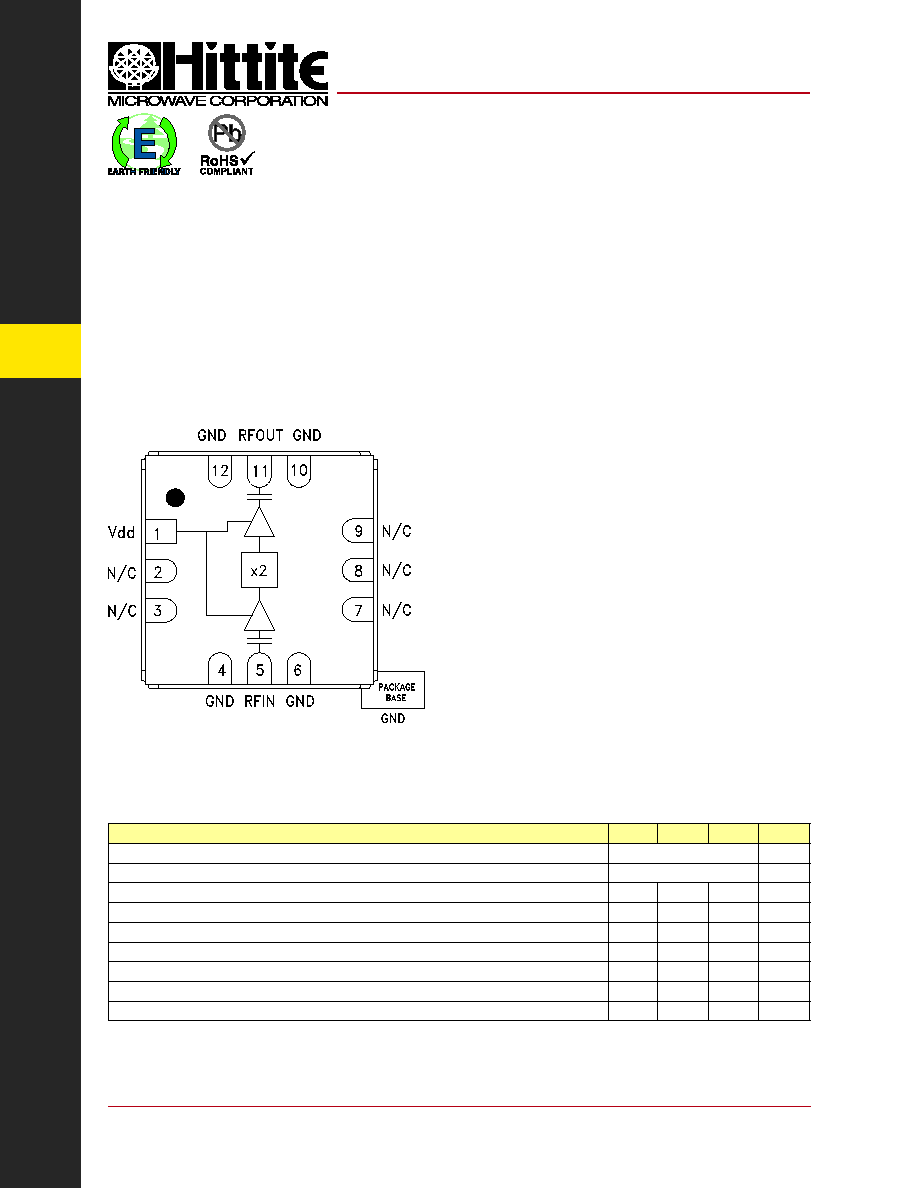
Pin Number
Function
Description
Interface Schematic
1
Vdd
Supply voltage 5V ± 0.5V. External bypass capacitors
of 100 pF, 1,000 pF and 2.2 F are required.
2, 3, 7-9
N/C
This pin may be connected to RF/DC ground.
Performance will not be affected.
4, 6, 10, 12
GND
Package bottom must also be connected
to RF/DC ground.
5
RFIN
Pin is AC coupled and matched to 50 Ohm
from 13.5 - 15.5 GHz.
11
RFOUT
Pin is AC coupled and matched to 50 Ohm
from 27 - 31 GHz.
HMC449LC3B
v00.0905
Pin Description
Application Circuit
Component
Value
C1
100 pF
C2
1,000 pF
C3
2.2 F
SMT GaAs MMIC x2 ACTIVE FREQUENCY
MULTIPLIER, 27 - 31 GHz OUTPUT