
MICROWAVE CORPORATION
8 - 268
For price, delivery, and to place orders, please contact Hittite Microwave Corporation:
12 Elizabeth Drive, Chelmsford, MA 01824 Phone: 978-250-3343 Fax: 978-250-3373
Order Online at www.hittite.com
AMPLIFIERS - SMT
8
HMC464LP5
GaAs PHEMT MMIC
POWER AMPLIFIER, 2.0 - 20.0 GHz
v00.0304
General Description
Features
Functional Diagram
The HMC464LP5 is a GaAs MMIC PHEMT Dis-
tributed Power Amplifi er in a leadless 5 x 5 mm
surface mount package which operates between
2 and 20 GHz. The amplifi er provides 14 dB of
gain, +30 dBm output IP3 and +26 dBm of output
power at 1 dB gain compression while requiring
290 mA from a +8V supply. Gain fl atness is good
from 2 - 18 GHz making the HMC464LP5 ideal
for EW, ECM and radar driver amplifi er as well as
test equipment applications. The wideband ampli-
fi er I/O's are internally matched to 50 Ohms.
+26 dBm P1dB Output Power
Gain: 14 dB
+30 dBm Output IP3
Supply Voltage: +8.0V @ 290 mA
50 Ohm Matched Input/Output
25 mm
2
Leadless SMT Package
Typical Applications
The HMC464LP5 wideband driver is ideal for:
� Telecom Infrastructure
� Microwave Radio & VSAT
� Military EW, ECM & C
3
I
� Test Instrumentation
� Fiber Optics
Electrical Specifi cations,
T
A
= +25� C, Vdd= 8V, Vgg2= 3V, Idd= 290 mA*
Parameter
Min.
Typ.
Max.
Min.
Typ.
Max.
Min.
Typ.
Max.
Units
Frequency Range
2.0 - 6.0
6.0 - 16.0
16.0 - 20.0
GHz
Gain
12
14
11.5
13.5
8
11
dB
Gain Flatness
�0.5
�0.5
�1.0
dB
Gain Variation Over Temperature
0.025
0.035
0.03
0.04
0.05
0.06
dB/ �C
Input Return Loss
15
10
7
dB
Output Return Loss
15
9
11
dB
Output Power for 1 dB Compression (P1dB)
23.5
26.5
22
25
18
21
dBm
Saturated Output Power (Psat)
27.5
26
24.0
dBm
Output Third Order Intercept (IP3)
32
26
22
dBm
Noise Figure
4.0
4.0
6.0
dB
Supply Current
(Idd) (Vdd= 8V, Vgg= -0.5V Typ.)
290
290
290
mA
* Adjust Vgg1 between -2 to 0V to achieve Idd= 290 mA typical.
MICROWAVE CORPORATION
8 - 269
For price, delivery, and to place orders, please contact Hittite Microwave Corporation:
12 Elizabeth Drive, Chelmsford, MA 01824 Phone: 978-250-3343 Fax: 978-250-3373
Order Online at www.hittite.com
AMPLIFIERS - SMT
8
GaAs MMIC SUB-HARMONICALLY PUMPED MIXER 17 - 25 GHz
HMC464LP5
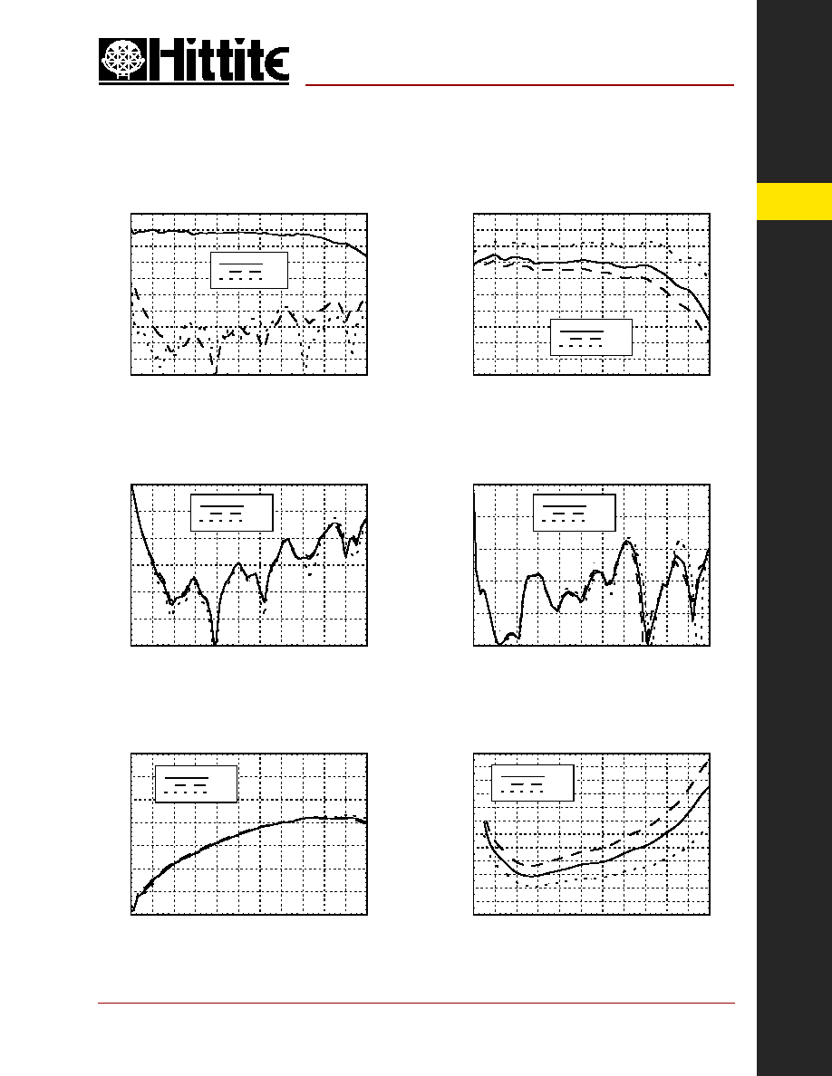
Output Return Loss vs. Temperature
v00.0304
Gain & Return Loss
Gain vs. Temperature
Reverse Isolation vs. Temperature
Input Return Loss vs. Temperature
GaAs PHEMT MMIC
POWER AMPLIFIER, 2.0 - 20.0 GHz
Noise Figure vs. Temperature
-30
-25
-20
-15
-10
-5
0
5
10
15
20
0
2
4
6
8
10
12
14
16
18
20
22
S21
S11
S22
RESPONSE (dB)
FREQUENCY (GHz)
0
2
4
6
8
10
12
14
16
18
20
0
2
4
6
8
10
12
14
16
18
20
22
+25C
+85C
-40C
GAIN
(dB)
FREQUENCY (GHz)
-30
-25
-20
-15
-10
-5
0
0
2
4
6
8
10
12
14
16
18
20
22
+25C
+85C
-40C
INPUT RETURN LOSS (dB)
FREQUENCY (GHz)
-25
-20
-15
-10
-5
0
0
2
4
6
8
10
12
14
16
18
20
22
+25C
+85C
-40C
OUTPUT RETURN LOSS (dB)
FREQUENCY (GHz)
-70
-60
-50
-40
-30
-20
-10
0
0
2
4
6
8
10
12
14
16
18
20
22
+25C
+85C
-40C
REVERSE ISOLATION (dB)
FREQUENCY (GHz)
0
1
2
3
4
5
6
7
8
9
10
11
12
0
2
4
6
8
10
12
14
16
18
20
22
+25C
+85C
-40C
NOI
SE FI
GURE (dB)
FREQUENCY (GHz)

MICROWAVE CORPORATION
8 - 270
For price, delivery, and to place orders, please contact Hittite Microwave Corporation:
12 Elizabeth Drive, Chelmsford, MA 01824 Phone: 978-250-3343 Fax: 978-250-3373
Order Online at www.hittite.com
AMPLIFIERS - SMT
8
HMC464LP5
v00.0304
GaAs PHEMT MMIC
POWER AMPLIFIER, 2.0 - 20.0 GHz
GaAs MMIC SUB-HARMONICALLY PUMPED MIXER 17 - 25 GHz
P1dB vs. Temperature
Psat vs. Temperature
Output IP3 vs. Temperature
Gain, Power & OIP3
vs. Supply Voltage @ 10 GHz, Fixed Vgg1
Absolute Maximum Ratings
Drain Bias Voltage (Vdd)
+9.0 Vdc
Gate Bias Voltage (Vgg1)
-2.0 to 0 Vdc
Gate Bias Voltage (Vgg2)
(Vdd -8.0) Vdc to Vdd
RF Input Power (RFin)(Vdd = +8.0 Vdc)
+23 dBm
Channel Temperature
150 �C
Continuous Pdiss (T= 85 �C)
(derate 51.5 mW/�C above 85 �C)
3.35 W
Thermal Resistance
(channel to ground paddle)
19.4 �C/W
Storage Temperature
-65 to +150 �C
Operating Temperature
-40 to +85 �C
Vdd (V)
Idd (mA)
+7.5
292
+8.0
290
+8.5
288
Typical Supply Current vs. Vdd
10
12
14
16
18
20
22
24
26
28
30
0
2
4
6
8
10
12
14
16
18
20
22
+25C
+85C
-40C
P1dB (dBm)
FREQUENCY (GHz)
10
12
14
16
18
20
22
24
26
28
30
0
2
4
6
8
10
12
14
16
18
20
22
+25C
+85C
-40C
Psat (dBm)
FREQUENCY (GHz)
16
18
20
22
24
26
28
30
32
34
36
0
2
4
6
8
10
12
14
16
18
20
22
+25C
+85C
-40C
OIP3 (dBm)
FREQUENCY (GHz)
10
12
14
16
18
20
22
24
26
28
30
32
7.5
8
8.5
Gain
P1dB
Psat
OIP3
Gain (dB), P1dB (dBm),
Psat (dBm), OIP3 (dBm)
SUPPLY VOLTAGE (Vdc)

MICROWAVE CORPORATION
8 - 271
For price, delivery, and to place orders, please contact Hittite Microwave Corporation:
12 Elizabeth Drive, Chelmsford, MA 01824 Phone: 978-250-3343 Fax: 978-250-3373
Order Online at www.hittite.com
AMPLIFIERS - SMT
8
HMC464LP5
v00.0304
GaAs PHEMT MMIC
POWER AMPLIFIER, 2.0 - 20.0 GHz
Outline Drawing
NOTES:
1. ALL DIMENSIONS IN INCHES [MILLIMETERS]
2. NO CONNECTION REQUIRED FOR UNLABELED BOND PADS
3. DIE THICKNESS IS 0.004 (0.100)
4. TYPICAL BOND PAD IS 0.004 (0.100) SQUARE
5. BACKSIDE METALLIZATION: GOLD
6. BACKSIDE METAL IS GROUND
7. BOND PAD METALIZATION: GOLD
Pad Number
Function
Description
Interface Schematic
5
RFIN
This pin is AC coupled and matched to 50 Ohms
from 2.0 - 20.0 GHz
15
Vgg1
Gate Control for amplifi er. Adjust between -2 to 0V
to achieve Idd= 290 mA.
21
RFOUT & Vdd
RF output for amplifi er. Connect the DC
bias (Vdd) network to provide drain current (Idd).
See application circuit herein.
30
Vgg2
Control voltage for amplifi er. +3V should be applied to
Vgg2 for nominal operation.
Ground
Paddle
GND
Ground paddle must be connected to RF/DC ground.
1-4, 6-14,
16-20, 22-29,
31, 32
N/C
No connection. These pins may be connected to RF ground.
Performance will not be affected.
Pad Descriptions

MICROWAVE CORPORATION
8 - 272
For price, delivery, and to place orders, please contact Hittite Microwave Corporation:
12 Elizabeth Drive, Chelmsford, MA 01824 Phone: 978-250-3343 Fax: 978-250-3373
Order Online at www.hittite.com
AMPLIFIERS - SMT
8
HMC464LP5
v00.0304
GaAs PHEMT MMIC
POWER AMPLIFIER, 2.0 - 20.0 GHz
Application Circuit
NOTE 1: Drain Bias (Vdd) must be applied through a broadband bias tee or external bias network.