Untitled-8
8
A
M
P
L
IF
IE
RS
-
S
M
T
8 - 402
For price, delivery, and to place orders, please contact Hittite Microwave Corporation:
20 Alpha Road, Chelmsford, MA 01824 Phone: 978-250-3343 Fax: 978-250-3373
Order On-line at www.hittite.com
HMC474MP86
SiGe HBT GAIN BLOCK
MMIC AMPLIFIER, DC - 6.0 GHz
v00.0305
General Description
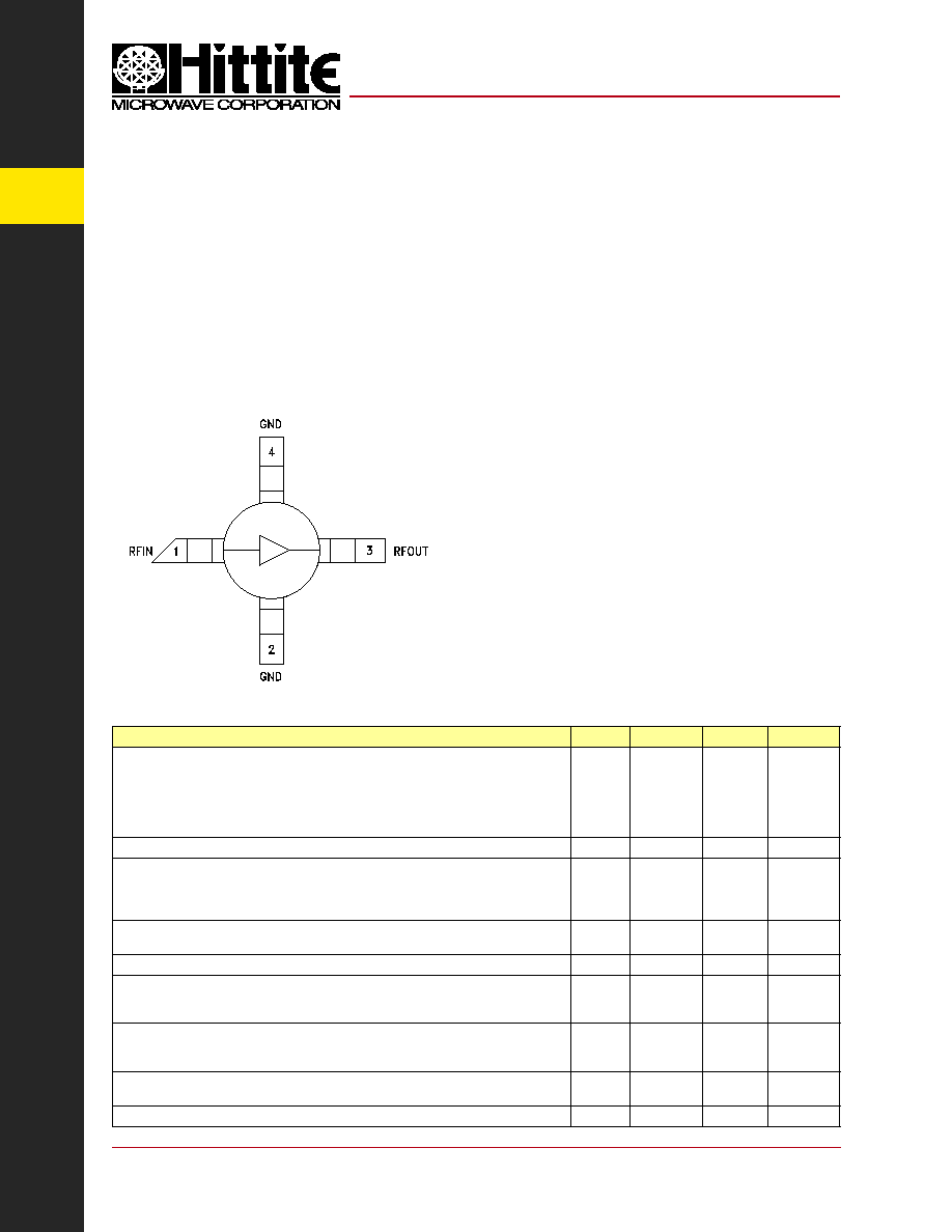
Functional Diagram
The HMC474MP86 is a general purpose SiGe
Heterojunction Bipolar Transistor (HBT) Gain
Block MMIC SMT amplifi er covering DC to 6 GHz.
This Micro-P packaged amplifi er can be used as a
cascadable 50 Ohm RF/IF gain stage with up to +10
dBm output power. The HMC474MP86 offers 15.5
dB of gain with a +22 dBm output IP3 at 850 MHz
while requiring only 25 mA from a single positive
supply. The Darlington feedback pair used results
in reduced sensitivity to normal process variations
and excellent gain stability over temperature
while requiring a minimal number of external bias
components.
Gain: 15.5 dB
P1dB Output Power: +8 dBm
Output IP3: +22 dBm
Cascadable 50 Ohm I/Os
Single Supply: +3V to +10V
Typical Applications
The HMC474MP86 is an ideal RF/IF gain block for:
· Cellular / PCS / 3G
· Fixed Wireless & WLAN
· CATV, Cable Modem & DBS
· Microwave Radio & Test Equipment
Electrical Specifi cations,
Vs= 5.0 V, Rbias= 110 Ohm, T
A
= +25° C
Parameter
Min.
Typ.
Max.
Units
Gain
DC - 1.0 GHz
1.0 - 2.0 GHz
2.0 - 3.0 GHz
3.0 - 4.0 GHz
4.0 - 5.0 GHz
5.0 - 6.0 GHz
13
12
10
9
8
7
15.5
14
12
11
10
9
dB
dB
dB
dB
dB
dB
Gain Variation Over Temperature
DC - 6.0 GHz
0.01
0.015
dB/ °C
Input Return Loss
DC - 1.0 GHz
1.0 - 4.0 GHz
4.0 - 5.0 GHz
5.0 - 6.0 GHz
15
16
19
16
dB
dB
dB
dB
Output Return Loss
DC - 5.0 GHz
5.0 - 6.0 GHz
17
13
dB
dB
Reverse Isolation
DC - 4.0 GHz
17
dB
Output Power for 1 dB Compression (P1dB)
0.5 - 4.0 GHz
4.0 - 5.0 GHz
5.0 - 6.0 GHz
5
4
3
8
7
6
dBm
dBm
dBm
Output Third Order Intercept (IP3)
(Pout= 0 dBm per tone, 1 MHz spacing)
0.5 - 4.0 GHz
4.0 - 5.0 GHz
5.0 - 6.0 GHz
22
20
17
dBm
dBm
dBm
Noise Figure
DC - 5.0 GHz
5.0 - 6.0 GHz
3
3.4
dB
dB
Supply Current (Icq)
25
mA
Note: Data taken with broadband bias tee on device output.
Features
8
A
M
P
L
IF
IE
RS
-
S
M
T
8 - 403
For price, delivery, and to place orders, please contact Hittite Microwave Corporation:
20 Alpha Road, Chelmsford, MA 01824 Phone: 978-250-3343 Fax: 978-250-3373
Order On-line at www.hittite.com
HMC474MP86
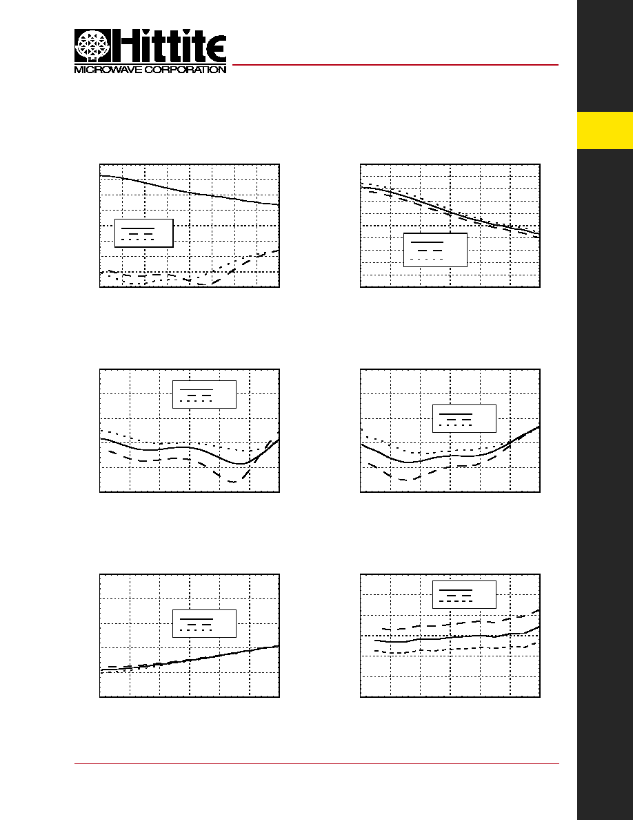
Output Return Loss vs. Temperature
v00.0305
Broadband Gain & Return Loss
Gain vs. Temperature
Reverse Isolation vs. Temperature
Input Return Loss vs. Temperature
SiGe HBT GAIN BLOCK
MMIC AMPLIFIER, DC - 6.0 GHz
Noise Figure vs. Temperature
-20
-15
-10
-5
0
5
10
15
20
0
1
2
3
4
5
6
7
8
S21
S11
S22
RESPONSE (dB)
FREQUENCY (GHz)
-25
-20
-15
-10
-5
0
0
1
2
3
4
5
6
+25 C
+85 C
-40 C
RETURN LOSS (dB)
FREQUENCY (GHz)
0
1
2
3
4
5
6
0
1
2
3
4
5
6
+25 C
+85 C
-40 C
NOI
SE FI
GURE (dB)
FREQUENCY (GHz)
-25
-20
-15
-10
-5
0
0
1
2
3
4
5
6
+25 C
+85 C
-40 C
REVERSE ISOLATION (dB)
FREQUENCY (GHz)
-25
-20
-15
-10
-5
0
0
1
2
3
4
5
6
+25 C
+85 C
-40 C
RETURN LOSS (dB)
FREQUENCY (GHz)
0
2
4
6
8
10
12
14
16
18
20
0
1
2
3
4
5
6
+25 C
+85 C
-40 C
GAIN
(dB)
FREQUENCY (GHz)
8
A
M
P
L
IF
IE
RS
-
S
M
T
8 - 404
For price, delivery, and to place orders, please contact Hittite Microwave Corporation:
20 Alpha Road, Chelmsford, MA 01824 Phone: 978-250-3343 Fax: 978-250-3373
Order On-line at www.hittite.com
HMC474MP86
v00.0305
SiGe HBT GAIN BLOCK
MMIC AMPLIFIER, DC - 6.0 GHz
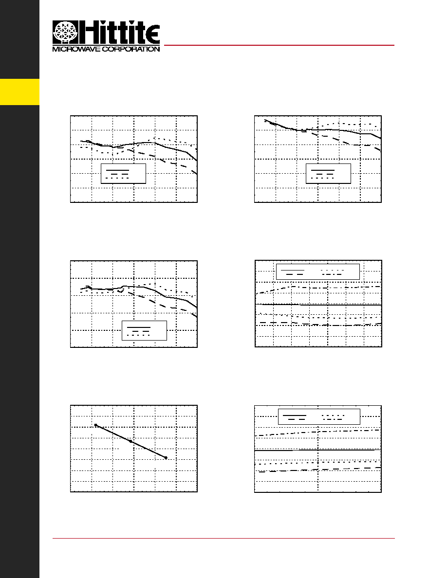
Gain, Power & OIP3 vs. Supply Voltage
for Constant Icc= 25 mA @ 850 MHz
P1dB vs. Temperature
Psat vs. Temperature
Output IP3 vs. Temperature
Vcc vs. Icc Over Temperature for
Fixed Vs= 5V, R
BIAS
= 110 Ohms
Gain, Power & OIP3 vs. Supply Voltage
for Rs = 110 Ohms @ 850 MHz
0
2
4
6
8
10
12
0
1
2
3
4
5
6
+25 C
+85 C
-40 C
P1dB (dBm)
FREQUENCY (GHz)
0
4
8
12
16
20
24
28
32
4.75
5
5.25
Gain
P1dB
Psat
OIP3
Gain (dB), P1dB (dBm),
Psat (dBm), OIP3 (dBm)
Vs (Vdc)
5
10
15
20
25
30
0
1
2
3
4
5
6
+25 C
+85 C
-40 C
OIP3 (dBm)
FREQUENCY (GHz)
20
21
22
23
24
25
26
27
28
2
2.1
2.2
2.3
2.4
2.5
2.6
I
cc (mA)
Vcc (Vdc)
+85 C
+25 C
-40 C
0
2
4
6
8
10
12
0
1
2
3
4
5
6
+25 C
+85 C
-40 C
Psat (dBm)
FREQUENCY (GHz)
0
4
8
12
16
20
24
28
32
3
4
5
6
7
8
9
10
Gain
P1dB
Psat
OIP3
Gain (dB), P1dB (dBm),
Psat (dBm), OIP3 (dBm)
Vs (Vdc)
8
A
M
P
L
IF
IE
RS
-
S
M
T
8 - 405
For price, delivery, and to place orders, please contact Hittite Microwave Corporation:
20 Alpha Road, Chelmsford, MA 01824 Phone: 978-250-3343 Fax: 978-250-3373
Order On-line at www.hittite.com
HMC474MP86
v00.0305
SiGe HBT GAIN BLOCK
MMIC AMPLIFIER, DC - 6.0 GHz
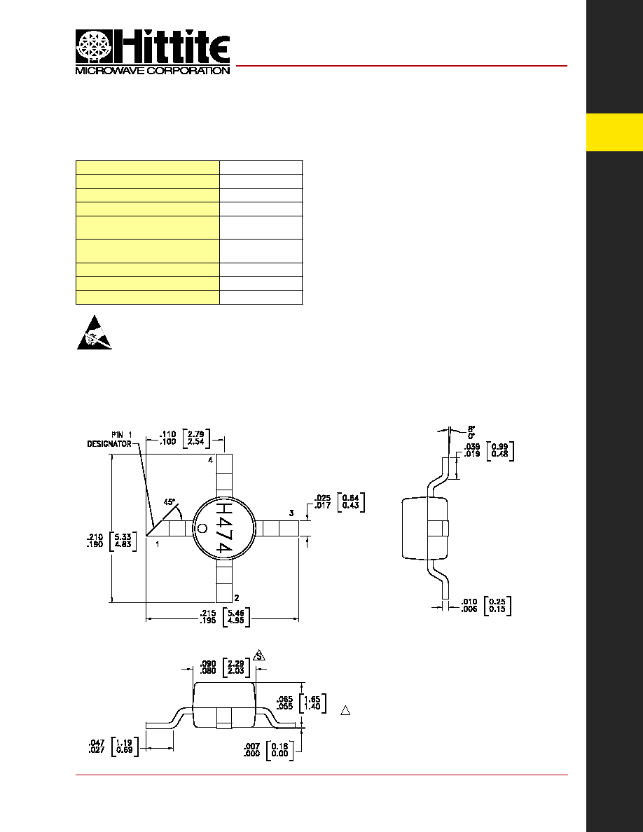
Outline Drawing
Absolute Maximum Ratings
Collector Bias Voltage (Vcc)
+6.0 Vdc
Collector Bias Current (Icc)
35 mA
RF Input Power (RFin)(Vcc = +2.4 Vdc)
+5 dBm
Junction Temperature
150 °C
Continuous Pdiss (T = 85 °C)
(derate 4.3 mW/°C above 85 °C)
0.280 W
Thermal Resistance
(junction to lead)
232 °C/W
Storage Temperature
-65 to +150 °C
Operating Temperature
-40 to +85 °C
ESD Sensitivity (HBM)
Class 1B
NOTES:
1. PACKAGE BODY MATERIAL: LOW STRESS INJECTION MOLDED
PLASTIC SILICA AND SILICON IMPREGNATED.
2. LEADFRAME MATERIAL: COPPER ALLOY
3. LEADFRAME PLATING: Sn/Pb SOLDER
4. DIMENSIONS ARE IN INCHES [MILLIMETERS].
5. DIMENSION DOES NOT INCLUDE MOLDFLASH OF 0.15mm PER SIDE.
6. ALL GROUND LEADS MUST BE SOLDERED TO PCB RF GROUND.
7. THE MICRO-P PACKAGE IS DIMENSIONALLY COMPATABLE WITH
THE "MICRO-X PACKAGE"
8. CLASSIFIED AS MOISTURE SENSITIVITY LEVEL (MSL) 1.
8
A
M
P
L
IF
IE
RS
-
S
M
T
8 - 406
For price, delivery, and to place orders, please contact Hittite Microwave Corporation:
20 Alpha Road, Chelmsford, MA 01824 Phone: 978-250-3343 Fax: 978-250-3373
Order On-line at www.hittite.com
HMC474MP86
v00.0305
SiGe HBT GAIN BLOCK
MMIC AMPLIFIER, DC - 6.0 GHz
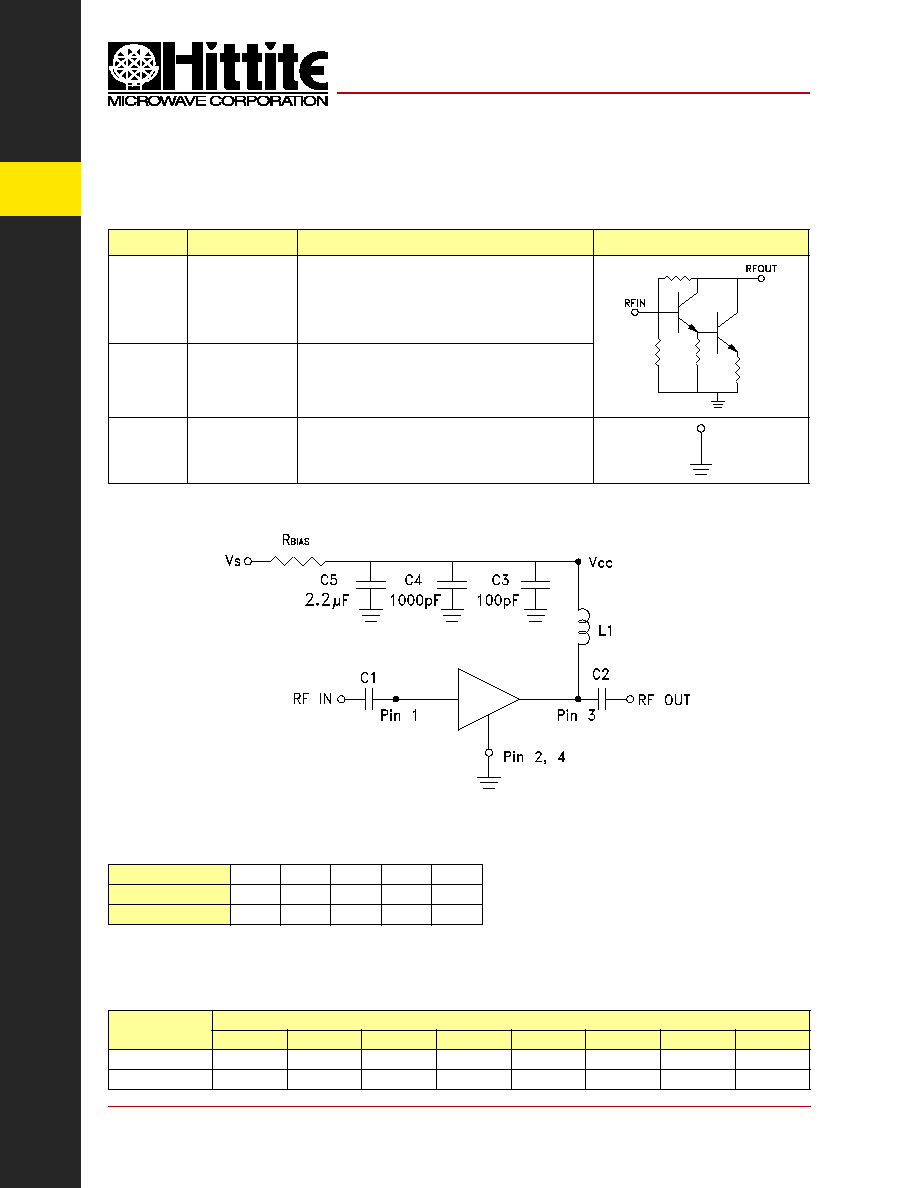
Application Circuit
Pin Descriptions
Pin Number
Function
Description
Interface Schematic
1
RFIN
This pin is DC coupled.
An off chip DC blocking capacitor is required.
3
RFOUT
RF output and DC Bias (Vcc) for the output stage.
2, 4
GND
These pins must be connected to RF/DC ground.
Recommended Component Values for Key Application Frequencies
Component
Frequency (MHz)
50
900
1900
2200
2400
3500
5200
5500
L1
270 nH
56 nH
18 nH
18 nH
15 nH
8.2 nH
6.8 nH
3.3 nH
C1, C2
0.01 µF
100 pF
100 pF
100 pF
100 pF
100 pF
100 pF
100 pF
Note:
1. External blocking capacitors are required on
RFIN and RFOUT.
2. R
BIAS
provides DC bias stability over temperature.
Recommended Bias Resistor Values
for Icc= 25 mA, Rbias= (Vs - Vcc) / Icc
Supply Voltage (Vs)
3V
5V
6V
8V
10V
R
BIAS
V
ALUE
30
110
150
240
300
R
BIAS
P
OWER
R
ATING
1/8 W
1/8 W
1/4 W
1/2 W
1/2 W