 | ÐлекÑÑоннÑй компоненÑ: HMC492LP3 | СкаÑаÑÑ:  PDF PDF  ZIP ZIP |
Äîêóìåíòàöèÿ è îïèñàíèÿ www.docs.chipfind.ru
MICROWAVE CORPORATION
10 - 118
For price, delivery, and to place orders, please contact Hittite Microwave Corporation:
12 Elizabeth Drive, Chelmsford, MA 01824 Phone: 978-250-3343 Fax: 978-250-3373
Order Online at www.hittite.com
FREQ.
DIVIDER & DETECT
ORS - SMT
10
HMC492LP3
SMT GaAs HBT MMIC
DIVIDE-BY-2, DC - 18 GHz
General Description
Features
Functional Diagram
The HMC492LP3 is a low noise Divide-by-2
Static Divider utilizing InGaP GaAs HBT technol-
ogy packaged in a leadless 3x3 mm QFN surface
mount plastic package. This device operates from
DC (with a square wave input) to 18 GHz input
frequency from a single +5.0V DC supply. The
low additive SSB phase noise of -150 dBc/Hz at
100 kHz offset helps the user maintain excellent
system noise performance.
Ultra Low SSB Phase Noise: -150 dBc/Hz
Very Wide Bandwidth
Output Power: -4 dBm
Single DC Supply: +5V
3 x 3 x 1 mm QFN SMT Package
Typical Applications
Prescaler for DC to 18 GHz PLL Applications:
· Point-to-Point / Multi-Point Radios
· VSAT Radios
· Fiber Optic
· Test Equipment
· Military
Electrical Specifi cations,
T
A
= +25° C, 50 Ohm System, Vcc= +5V
1. Divider will operate down to DC for square-wave input signal.
v01.0604
Parameter
Conditions
Min.
Typ.
Max.
Units
Maximum Input Frequency
18
19
GHz
Minimum Input Frequency
Sine Wave Input. [1]
0.2
0.5
GHz
Input Power Range
Fin = 2 to 14 GHz
-15
-20
+10
dBm
Fin = 14 to 16 GHz
-15
-20
+5
dBm
Fin = 16 to 18 GHz
-10
-15
0
dBm
Output Power
Fin = 0.5 to 18 GHz
-7
-4
dBm
Reverse Leakage
Both RF Outputs Terminated
60
dB
SSB Phase Noise (100 kHz offset)
Pin = 0 dBm, Fin = 4.8 GHz
-150
dBc/Hz
Output Transition Time
Pin = 0 dBm, Fout = 882 MHz
100
ps
Supply Current (Icc1 + Icc2)
78
mA
MICROWAVE CORPORATION
10 - 119
For price, delivery, and to place orders, please contact Hittite Microwave Corporation:
12 Elizabeth Drive, Chelmsford, MA 01824 Phone: 978-250-3343 Fax: 978-250-3373
Order Online at www.hittite.com
10
FREQ.
DIVIDERS & DETECT
ORS - SMT
GaAs MMIC SUB-HARMONICALLY PUMPED MIXER 17 - 25 GHz
HMC492LP3
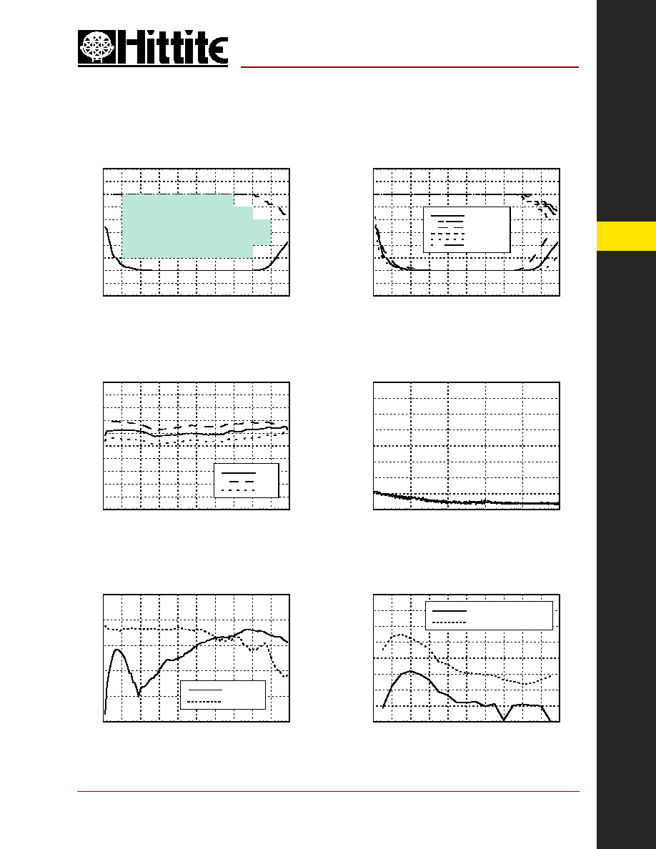
SSB Phase Noise Performance,
Pin= 0 dBm, T= 25 °C
Input Sensitivity Window, T= 25 °C
Input Sensitivity Window vs. Temperature
SMT GaAs HBT MMIC
DIVIDE-BY-2, DC - 18 GHz
Output Power vs. Temperature
Reverse Leakage, Pin= 0 dBm, T= 25 °C
Output Harmonic Content,
Pin= 0 dBm, T= 25 °C
v01.0604
-30
-20
-10
0
10
20
0
2
4
6
8
10
12
14
16
18
20
INPUT POWER (dBm)
INPUT FREQUENCY (GHz)
Recommended
Operating Window
-30
-20
-10
0
10
20
0
2
4
6
8
10
12
14
16
18
20
Min Pin +25C
Max Pin +25C
Min Pin +85C
Max Pin +85C
Min Pin -40C
Max Pin -40C
INPUT POWER (dBm)
INPUT FREQUENCY (GHz)
-10
-9
-8
-7
-6
-5
-4
-3
-2
-1
0
0
2
4
6
8
10
12
14
16
18
20
+25C
+85C
-40C
OUTPUT POWER (dBm)
INPUT FREQUENCY (GHz)
-160
-140
-120
-100
-80
-60
-40
-20
0
10
2
10
3
10
4
10
5
10
6
10
7
SSB PHASE NOISE (dBc/Hz)
OFFSET FREQUENCY (Hz)
-50
-40
-30
-20
-10
0
0
2
4
6
8
10
12
14
16
18
20
Pfeedthru
3rd Harmonic
OUTPUT LEVEL (dBm)
INPUT FREQUENCY (GHz)
-80
-70
-60
-50
-40
-30
-20
-10
0
0
2
4
6
8
10
12
14
16
18
20
Both Output Ports Terminated
One Output Port Terminated
OUTPUT LEVEL (dBm)
INPUT FREQUENCY (GHz)
MICROWAVE CORPORATION
10 - 120
For price, delivery, and to place orders, please contact Hittite Microwave Corporation:
12 Elizabeth Drive, Chelmsford, MA 01824 Phone: 978-250-3343 Fax: 978-250-3373
Order Online at www.hittite.com
FREQ.
DIVIDER & DETECT
ORS - SMT
10
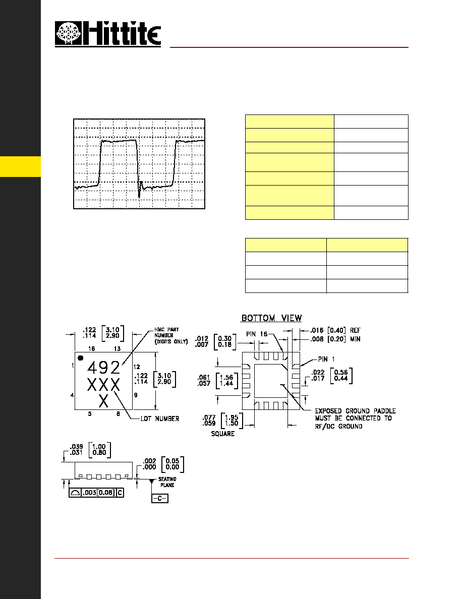
Output Voltage Waveform,
Pin= 0 dBm, Fout= 882 MHz, T= 25 °C
SMT GaAs HBT MMIC
DIVIDE-BY-2, DC - 18 GHz
HMC492LP3
Absolute Maximum Ratings
Outline Drawing
Typical Supply Current vs. Vcc
Note: Divider will operate over full voltage range shown above
v01.0604
RF Input (Vcc = +5V)
+13 dBm
Supply Voltage (Vcc1, Vcc2)
+5.5V
Channel Temperature (Tc)
135 °C
Continuous Pdiss (T = 85 °C)
(derate 11.9 mW/° C above 85 °C)
593 mW
Storage Temperature
-65 to +150 °C
Thermal Resistance (R
TH
)
(junction to ground paddle)
84 °C/W
Operating Temperature
-40 to +85 °C
-500
-400
-300
-200
-100
0
100
200
300
400
500
23.5 23.7 23.9 24.1 24.3 24.5 24.7 24.9 25.1 25.3 25.5
AMPLITUDE (mV)
TIME (nS)
NOTES:
1. MATERIAL PACKAGE BODY: LOW STRESS INJECTION MOLDED
PLASTIC SILICA AND SILICON IMPREGNATED.
2. LEAD AND GROUND PADDLE MATERIAL: COPPER ALLOY
3. LEAD AND GROUND PADDLE PLATING: Sn/Pb SOLDER
4. DIMENSIONS ARE IN INCHES [MILLIMETERS].
5. LEAD SPACING TOLERANCE IS NON-CUMULATIVE
6. PAD BURR LENGTH SHALL BE 0.15mm MAXIMUM.
PAD BURR HEIGHT SHALL BE 0.05mm MAXIMUM.
7. PACKAGE WARP SHALL NOT EXCEED 0.05mm.
8. ALL GROUND LEADS AND GROUND PADDLE MUST BE SOLDERED
TO PCB RF GROUND.
9. REFER TO HITTITE APPLICATION NOTE FOR SUGGESTED PCB
LAND
PATTERN.
Vcc1, Vcc2 (V)
Icc (mA)
4.75
69
5.0
78
5.25
87
MICROWAVE CORPORATION
10 - 121
For price, delivery, and to place orders, please contact Hittite Microwave Corporation:
12 Elizabeth Drive, Chelmsford, MA 01824 Phone: 978-250-3343 Fax: 978-250-3373
Order Online at www.hittite.com
10
FREQ.
DIVIDERS & DETECT
ORS - SMT
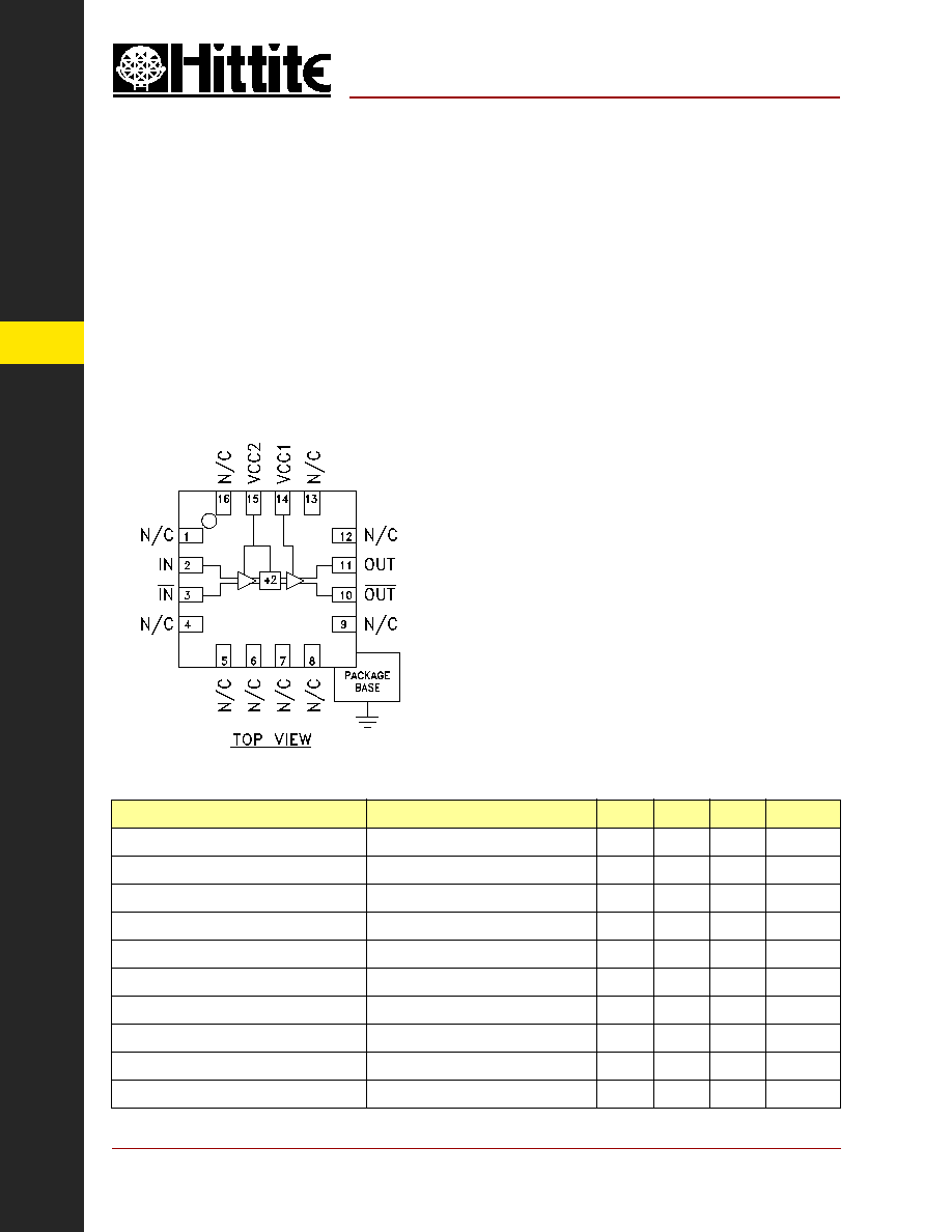
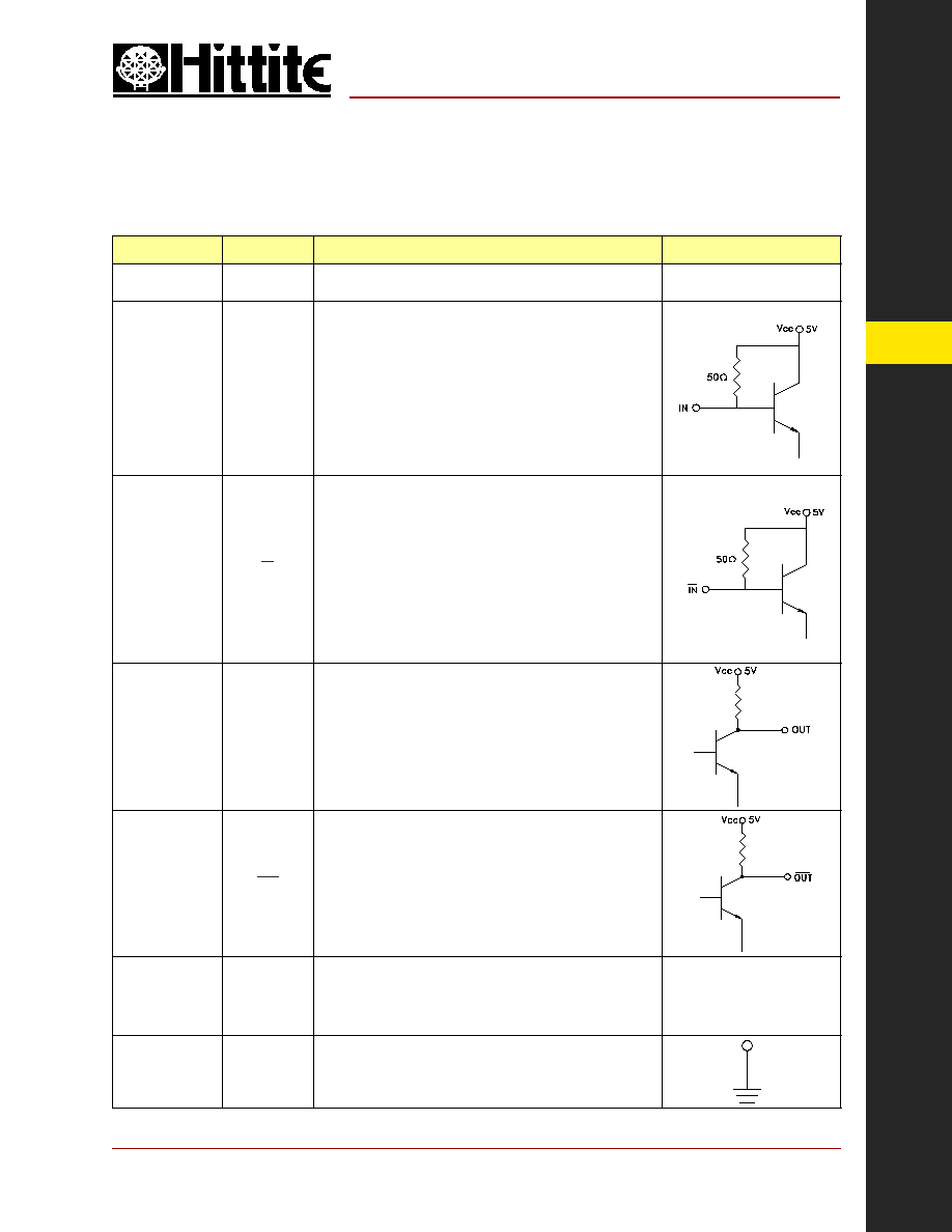
Pin Number
Function
Description
Interface Schematic
1, 4-9, 12, 13, 16
N/C
No connection.
2
IN
RF Input must be DC blocked.
3
IN
RF Input 180° out of phase with pin 2 for differential operation.
AC ground for single ended operation.
10
OUT
Divided Output.
11
OUT
Divided output 180° out of phase with pin 10.
14, 15
Vcc1, Vcc2
Supply voltage 5V ± 0.25V. Connect both pins to +5V supply.
GND
Ground: Backside of package has exposed metal ground slug which
must be connected to RF/DC ground.
SMT GaAs HBT MMIC
DIVIDE-BY-2, DC - 18 GHz
HMC492LP3
Pin Description
v01.0604
MICROWAVE CORPORATION
10 - 122
For price, delivery, and to place orders, please contact Hittite Microwave Corporation:
12 Elizabeth Drive, Chelmsford, MA 01824 Phone: 978-250-3343 Fax: 978-250-3373
Order Online at www.hittite.com
FREQ.
DIVIDER & DETECT
ORS - SMT
10
SMT GaAs HBT MMIC
DIVIDE-BY-2, DC - 18 GHz
HMC492LP3
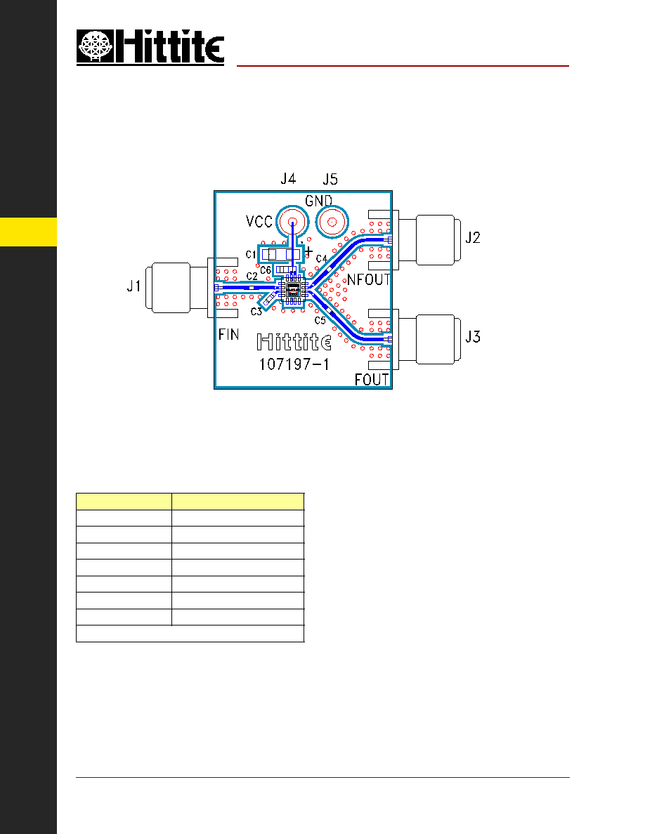
Evaluation PCB
List of Materials
The circuit board used in the fi nal application should use
RF circuit design techniques. Signal lines should have
50 ohm impedance while the package ground leads
and backside ground slug should be connected directly
to the ground plane similar to that shown. A suffi cient
number of via holes should be used to connect the top
and bottom ground planes. The evaluation circuit board
shown is available from Hittite upon request. This evalu-
ation board is designed for single ended input testing. J2
and J3 provide differential output signals.
v01.0604
Item
Description
J1 - J3
PC Mount SMA RF Connector
J4, J5
DC Pin
C2 - C5
100 pF Capacitor, 0402 Pkg.
C6
1000 pF Capacitor, 0603 Pkg.
C1
2.2 uF Tantalum Capacitor
U1
HMC492LP3 Divide-by-2
PCB*
107197 Eval Board
* Circuit Board Material: Rogers 4350