VC
O
S
& P
L
Os - SM
T
11
11 - 126
For price, delivery, and to place orders, please contact Hittite Microwave Corporation:
20 Alpha Road, Chelmsford, MA 01824 Phone: 978-250-3343 Fax: 978-250-3373
Order On-line at www.hittite.com
HMC511LP5
/
511LP5E
MMIC VCO w/ HALF FREQUENCY
OUTPUT 9.05 - 10.15 GHz
v00.0506
General Description
Features
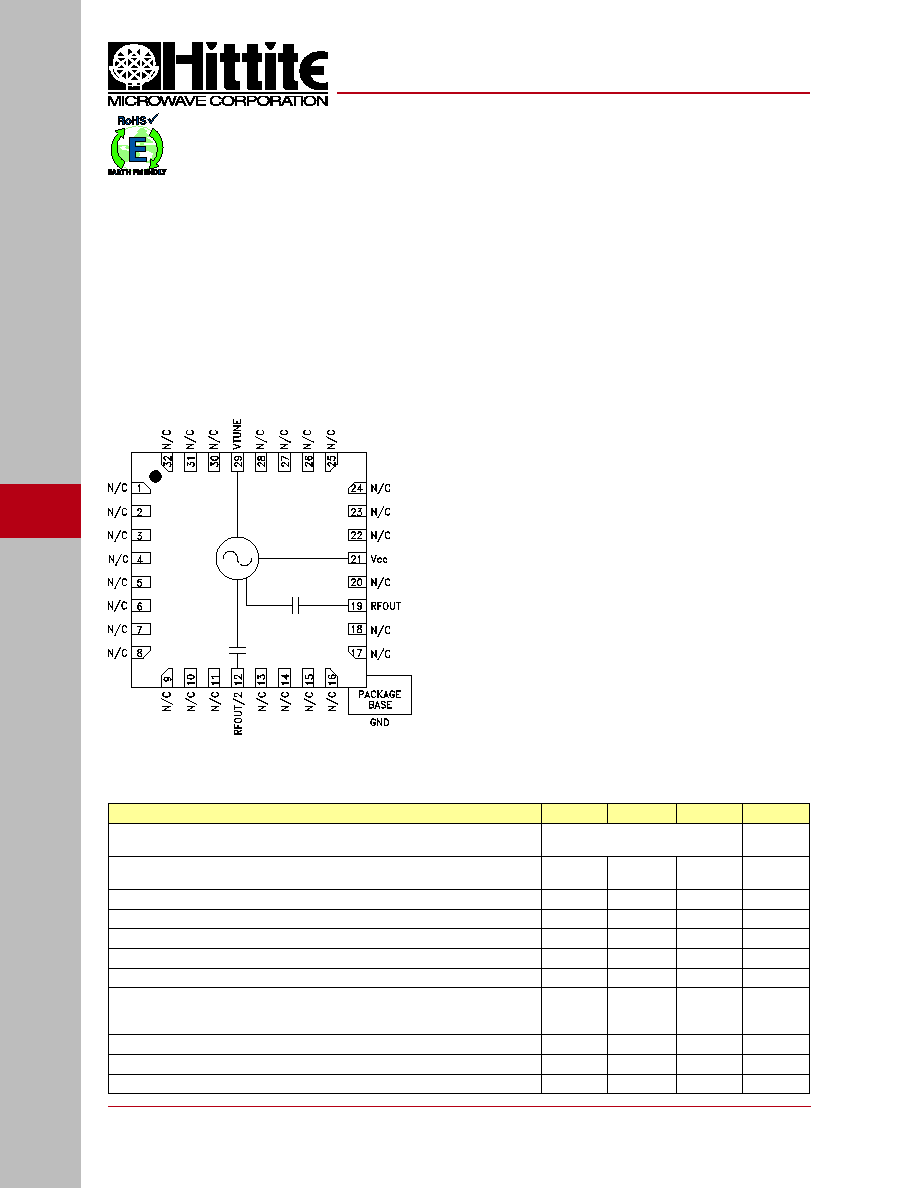
Functional Diagram
The HMC511LP5 & HMC511LP5E are GaAs InGaP
Heterojunction Bipolar Transistor (HBT) MMIC VCOs.
The HMC511LP5 & HMC511LP5E integrate resonators,
negative resistance devices, varactor diodes and
feature a half frequency output. The VCO's phase
noise performance is excellent over temperature,
shock, and process due to the oscillator's monolithic
structure. Power output is +13 dBm typical from a +5V
supply. The voltage controlled oscillator is packaged
in a leadless QFN 5x5 mm surface mount package,
and requires no external matching components.
Dual Output: Fo = 9.05 - 10.15 GHz
Fo/2 = 4.525 - 5.075 GHz
Pout: +13 dBm
Phase Noise: -115 dBc/Hz @100 kHz Typ.
No External Resonator Needed
QFN Leadless SMT Package, 25 mm
2
Typical Applications
Low noise MMIC VCO w/Half Frequency, for:
� VSAT Radio
� Point to Point/Multi-Point Radio
� Test Equipment & Industrial Controls
� Military End-Use
Electrical Specifications,
T
A
= +25� C, Vcc = +5V
Parameter
Min.
Typ.
Max.
Units
Frequency Range
Fo
Fo/2
9.05 - 10.15
4.525 - 5.075
GHz
GHz
Power Output
RFOUT
RFOUT/2
+9
+5
+16
+11
dBm
dBm
SSB Phase Noise @ 100 kHz Offset, Vtune= +5V @ RFOUT
-115
dBc/Hz
Tune Voltage
Vtune
2
13
V
Supply Current (Icc) (Vcc = +5.0V)
200
265
300
mA
Tune Port Leakage Current (Vtune= 13V)
10
A
Output Return Loss
2
dB
Harmonics/Subharmonics
1/2
2nd
3rd
38
15
30
dBc
dBc
dBc
Pulling (into a 2.0:1 VSWR)
8
MHz pp
Pushing @ Vtune= 5V
15
MHz/V
Frequency Drift Rate
0.9
MHz/�C

VC
O
S
& P
L
Os - SM
T
11
11 - 127
For price, delivery, and to place orders, please contact Hittite Microwave Corporation:
20 Alpha Road, Chelmsford, MA 01824 Phone: 978-250-3343 Fax: 978-250-3373
Order On-line at www.hittite.com
Frequency vs. Tuning Voltage, T= 25�C
Sensitivity vs. Tuning Voltage, Vcc= +5V
SSB Phase Noise @ Vtune = +5V
Frequency vs. Tuning Voltage, Vcc= +5V
Output Power
vs. Tuning Voltage, Vcc= +5V
7.8
8
8.2
8.4
8.6
8.8
9
9.2
9.4
9.6
9.8
10
10.2
10.4
10.6
0
1
2
3
4
5
6
7
8
9
10
11
12
13
Vcc=4.75V
Vcc=5.0V
Vcc=5.25V
OUTPUT FREQUENCY (GHz)
TUNING VOLTAGE (VOLTS)
HMC511LP5
/
511LP5E
v00.0506
0
2
4
6
8
10
12
14
16
18
20
0
1
2
3
4
5
6
7
8
9
10
11
12
13
+25 C
+85 C
-40 C
OUTPUT POWER (dBm)
TUNING VOLTAGE (VOLTS)
0
50
100
150
200
250
300
350
400
450
500
550
600
650
0
1
2
3
4
5
6
7
8
9
10
11
12
13
+25 C
+85 C
-40 C
SENSITIVITY (MHz/V)
TUNING VOLTAGE (VOLTS)
-160
-140
-120
-100
-80
-60
-40
-20
0
10
2
10
3
10
4
10
5
10
6
+25 C
+85 C
-40 C
SSB PHASE NOISE (dBc/Hz)
OFFSET FREQUENCY (Hz)
7.8
8
8.2
8.4
8.6
8.8
9
9.2
9.4
9.6
9.8
10
10.2
10.4
10.6
0
1
2
3
4
5
6
7
8
9
10
11
12
13
+25 C
+85 C
-40 C
OUTPUT FREQUENCY (GHz)
TUNING VOLTAGE (VOLTS)
MMIC VCO w/ HALF FREQUENCY
OUTPUT 9.05 - 10.15 GHz
SSB Phase Noise vs. Tuning Voltage
-130
-120
-110
-100
-90
-80
-70
-60
-50
-40
-30
-20
-10
0
1
2
3
4
5
6
7
8
9
10
11
12
13
10kHz offset
100kHz offset
SSB PHASE NOISE (dBc/Hz)
TUNING VOLTAGE (VOLTS)

VC
O
S
& P
L
Os - SM
T
11
11 - 128
For price, delivery, and to place orders, please contact Hittite Microwave Corporation:
20 Alpha Road, Chelmsford, MA 01824 Phone: 978-250-3343 Fax: 978-250-3373
Order On-line at www.hittite.com
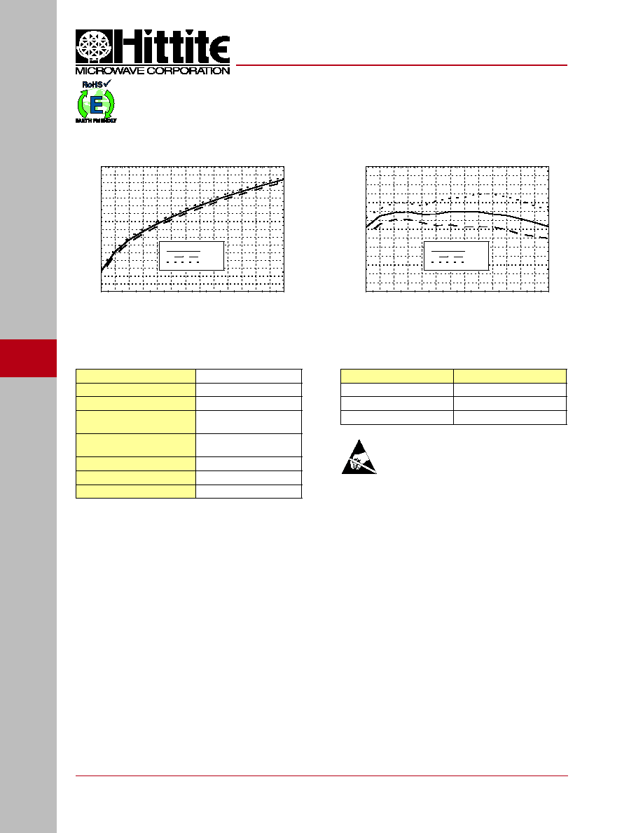
Absolute Maximum Ratings
Vcc
+5.5 Vdc
Vtune
0 to +15V
Junction Temperature
135 �C
Continuous Pdiss (T=85 �C)
(derate 31.5 mW/C above 85 �C
1.58 W
Thermal Resistance
(junction to ground paddle)
31.6 �C/W
Storage Temperature
-65 to +150 �C
Operating Temperature
-40 to +85 �C
ESD Sensitivity (HBM)
Class 1A
Typical Supply Current vs. Vcc
Note: VCO will operate over full voltage range shown above.
Vcc (V)
Icc (mA)
4.75
245
5.0
265
5.25
285
ELECTROSTATIC SENSITIVE DEVICE
OBSERVE HANDLING PRECAUTIONS
RFOUT/2 Frequency
vs. Tuning Voltage, Vcc= +5V
RFOUT/2 Output Power
vs. Tuning Voltage, Vcc= +5V
0
1
2
3
4
5
6
7
8
9
10
11
12
13
14
0
1
2
3
4
5
6
7
8
9
10
11
12
13
+25 C
+85 C
-40 C
OUTPUT POWER (dBm)
TUNING VOLTAGE (VOLTS)
3.8
3.9
4
4.1
4.2
4.3
4.4
4.5
4.6
4.7
4.8
4.9
5
5.1
5.2
5.3
5.4
0
1
2
3
4
5
6
7
8
9
10
11
12
13
+25 C
+85 C
-40 C
OUTPUT FREQUENCY (GHz)
TUNING VOLTAGE (VOLTS)
HMC511LP5
/
511LP5E
v00.0506
MMIC VCO w/ HALF FREQUENCY
OUTPUT 9.05 - 10.15 GHz

VC
O
S
& P
L
Os - SM
T
11
11 - 129
For price, delivery, and to place orders, please contact Hittite Microwave Corporation:
20 Alpha Road, Chelmsford, MA 01824 Phone: 978-250-3343 Fax: 978-250-3373
Order On-line at www.hittite.com
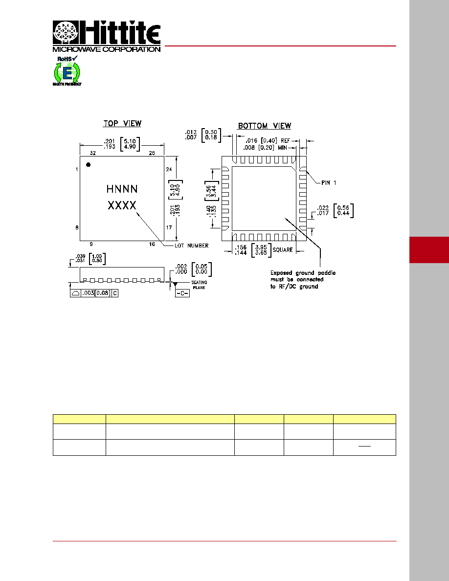
Outline Drawing
NOTES:
1. LEADFRAME MATERIAL: COPPER ALLOY
2. DIMENSIONS ARE IN INCHES [MILLIMETERS]
3. LEAD SPACING TOLERANCE IS NON-CUMULATIVE.
4. PAD BURR LENGTH SHALL BE 0.15mm MAXIMUM.
PAD BURR HEIGHT SHALL BE 0.05mm MAXIMUM.
5. PACKAGE WARP SHALL NOT EXCEED 0.05mm.
6. ALL GROUND LEADS AND GROUND PADDLE MUST BE
SOLDERED TO PCB RF GROUND.
7. REFER TO HITTITE APPLICATION NOTE FOR SUGGESTED
LAND PATTERN.
Part Number
Package Body Material
Lead Finish
MSL Rating
Package Marking
[3]
HMC511LP5
Low Stress Injection Molded Plastic
Sn/Pb Solder
MSL1
[1]
H511
XXXX
HMC511LP5E
RoHS-compliant Low Stress Injection Molded Plastic
100% matte Sn
MSL1
[2]
H511
XXXX
[1] Max peak refl ow temperature of 235 �C
[2] Max peak refl ow temperature of 260 �C
[3] 4-Digit lot number XXXX
Package Information
HMC511LP5
/
511LP5E
v00.0506
MMIC VCO w/ HALF FREQUENCY
OUTPUT 9.05 - 10.15 GHz

VC
O
S
& P
L
Os - SM
T
11
11 - 130
For price, delivery, and to place orders, please contact Hittite Microwave Corporation:
20 Alpha Road, Chelmsford, MA 01824 Phone: 978-250-3343 Fax: 978-250-3373
Order On-line at www.hittite.com
Pin Number
Function
Description
Interface Schematic
1-11, 13-18,
20, 22-28,
30-32
N/C
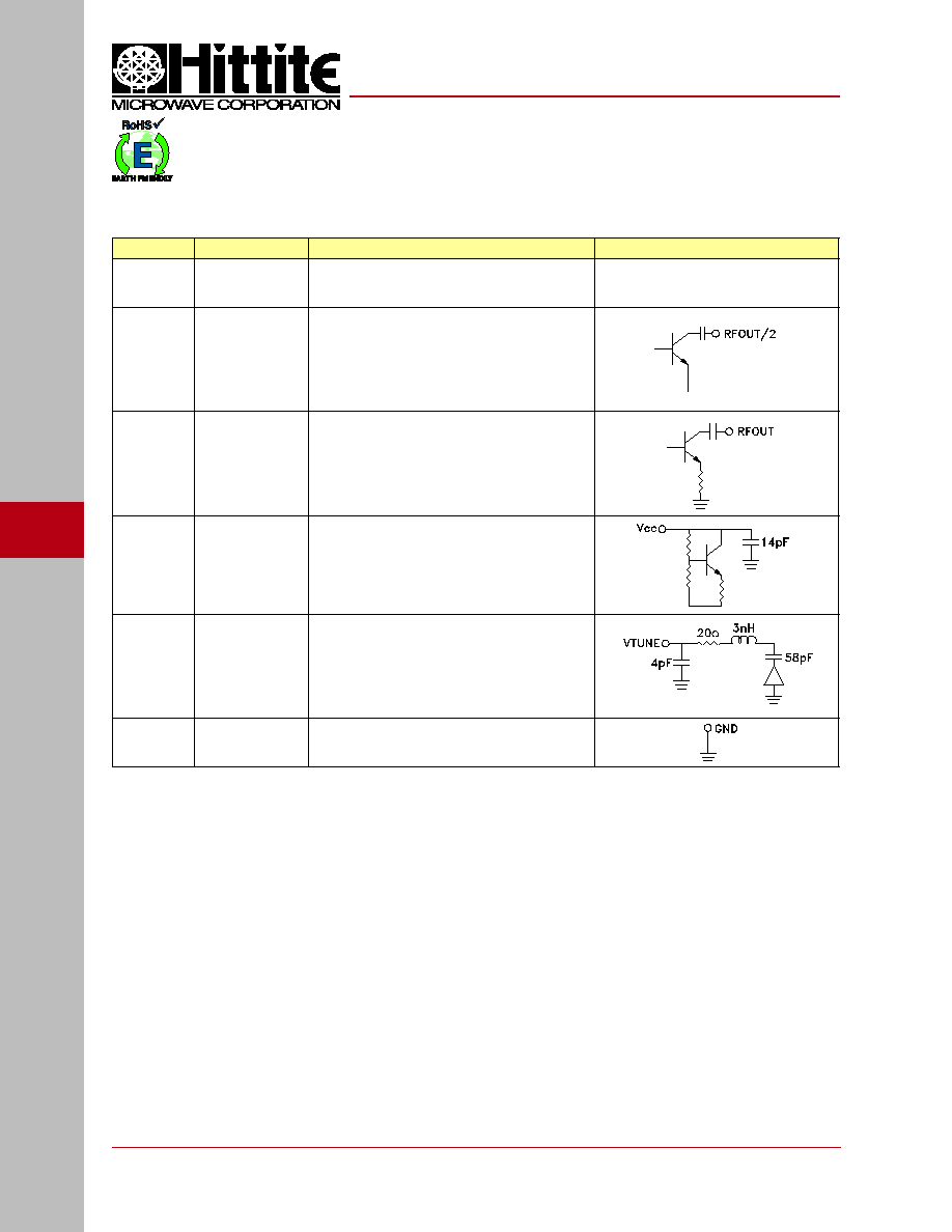
No Connection. These pins may be connected to RF/
DC ground. Performance will not be affected.
12
RFOUT/2
Half frequency output (AC coupled).
19
RFOUT
RF output (AC coupled).
21
Vcc
Supply Voltage, +5V
29
VTUNE
Control Voltage Input. Modulation port bandwidth
dependent on drive source impedance.
GND
Package bottom has an exposed metal paddle
that must be connected to RF/DC ground.
Pin Descriptions
HMC511LP5
/
511LP5E
v00.0506
MMIC VCO w/ HALF FREQUENCY
OUTPUT 9.05 - 10.15 GHz

VC
O
S
& P
L
Os - SM
T
11
11 - 131
For price, delivery, and to place orders, please contact Hittite Microwave Corporation:
20 Alpha Road, Chelmsford, MA 01824 Phone: 978-250-3343 Fax: 978-250-3373
Order On-line at www.hittite.com
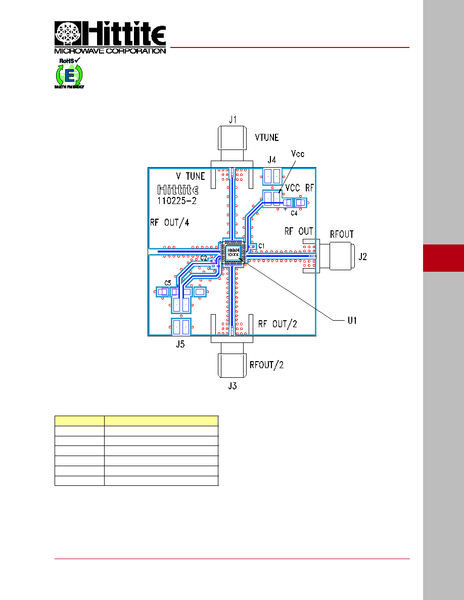
The circuit board used in the fi nal application should
use RF circuit design techniques. Signal lines should
have 50 ohm impedance while the package ground
leads and backside ground paddle should be con-
nected directly to the ground plane similar to that
shown. A suffi cient number of via holes should be
used to connect the top and bottom ground planes.
The evaluation circuit board shown is available from
Hittite upon request.
Evaluation PCB
List of Materials for Evaluation PCB 110227
[1]
Item
Description
J1 - J3
PCB Mount SMA RF Connector
J4, J5
2 mm DC Header
C1 - C2
100 pF Capacitor, 0402 Pkg.
C4 - C5
2.2 F Tantalum Capacitor
U1
HMC511LP5 / HMC511LP5E VCO
PCB
[2]
110225 Eval Board
[1] Reference this number when ordering complete evaluation PCB
[2] Circuit Board Material: Rogers 4350
HMC511LP5
/
511LP5E
v00.0506
MMIC VCO w/ HALF FREQUENCY
OUTPUT 9.05 - 10.15 GHz
