5
M
I
X
E
R
S
- C
H
I
P
5 - 170
For price, delivery, and to place orders, please contact Hittite Microwave Corporation:
20 Alpha Road, Chelmsford, MA 01824 Phone: 978-250-3343 Fax: 978-250-3373
Order On-line at www.hittite.com
HMC527
GaAs MMIC I/Q MIXER
8.5 - 13.5 GHz
v00.1204
General Description
Features
Typical Applications
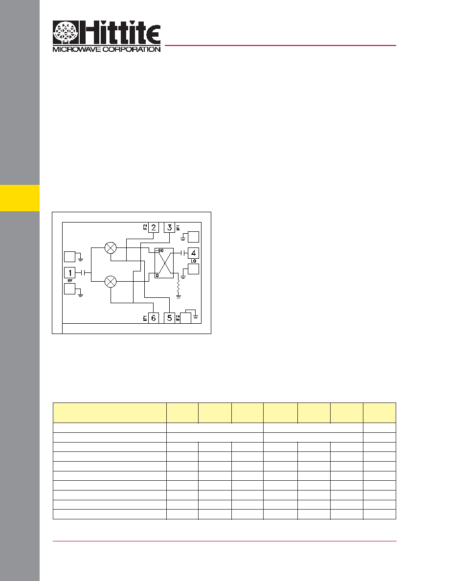
The HMC527 is a compact I /Q MMIC mixer which
can be used as either an Image Reject Mixer or a
Single Sideband Upconverter. The chip utilizes two
standard Hittite double balanced mixer cells and a
90 degree hybrid fabricated in a GaAs MESFET
process. All data shown below is taken with the chip
mounted in a 50 Ohm test fi xture and includes the
effects of 1 mil diameter x 20 mil length bond wires
on each port. A low frequency quadrature hybrid
was used to produce a 100 MHz USB IF output.
This product is a much smaller alternative to hybrid
style Image Reject Mixers and Single Sideband
Upconverter assemblies.
Electrical Specifi cations,
T
A
= +25� C, IF= 100 MHz, LO = +19 dBm*
* Unless otherwise noted, all measurements performed as downconverter.
Parameter
Min.
Typ.
Max.
Min.
Typ.
Max.
Units
Frequency Range, RF/LO
8.5 - 13.5
10.5 - 12
GHz
Frequency Range, IF
DC - 2
DC - 2
GHz
Conversion Loss (As IRM)
8
10
7.5
9.5
dB
Image Rejection
17
25
27
35
dB
1 dB Compression (Input)
+21
+21
dBm
LO to RF Isolation
35
45
45
50
dB
LO to IF Isolation
17
22
19
24
dB
IP3 (Input)
+25
+28
dBm
Amplitude Balance
0.7
0.5
dB
Phase Balance
6
6
Deg
Functional Diagram
The HMC527 is ideal for:
� Point-to-Point and Point-to-Multi-Point Radio
� VSAT
Wide IF Bandwidth: DC - 2 GHz
Image Rejection: 35 dB
LO to RF Isolation: 50 dB
High Input IP3: +28 dBm
5
M
I
X
E
R
S
- C
H
I
P
5 - 171
For price, delivery, and to place orders, please contact Hittite Microwave Corporation:
20 Alpha Road, Chelmsford, MA 01824 Phone: 978-250-3343 Fax: 978-250-3373
Order On-line at www.hittite.com
HMC527
GaAs MMIC I/Q MIXER
8.5 - 13.5 GHz
v00.1204
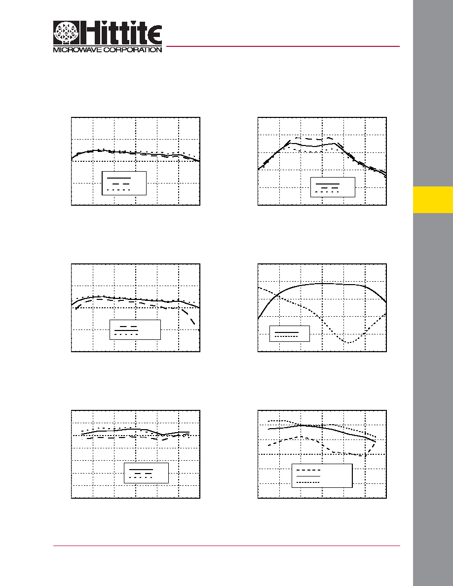
Conversion Gain vs. Temperature
Image Rejection vs. Temperature
Conversion Gain vs. LO Drive
Return Loss
Data taken as IRM with External IF Hybrid
-20
-15
-10
-5
0
8
9
10
11
12
13
14
+25C
+85C
-55C
CONVERSION GAIN (dB)
RF FREQUENCY (GHz)
Input P1dB vs. Temperature
Input IP3 vs. LO Drive
0
10
20
30
40
50
8
9
10
11
12
13
14
+25C
+85C
-55C
I
M
AGE REJECTI
ON (dB)
RF FREQUENCY (GHz)
-20
-15
-10
-5
0
8
9
10
11
12
13
14
+17 dBm
+19 dBm
+21 dBm
CONVERSION GAIN (dB)
RF FREQUENCY (GHz)
-25
-20
-15
-10
-5
0
8
9
10
11
12
13
14
RF
LO
RETURN LOSS (dB)
FREQUENCY (GHz)
10
12
14
16
18
20
22
24
8
9
10
11
12
13
14
+25C
+85C
-55C
P1dB (dBm)
RF FREQUENCY (GHz)
5
10
15
20
25
30
35
8
9
10
11
12
13
14
LO = +17 dBm
LO = +19 dBm
LO = +21 dBm
IP3 (dBm)
RF FREQUENCY (GHz)

5
M
I
X
E
R
S
- C
H
I
P
5 - 172
For price, delivery, and to place orders, please contact Hittite Microwave Corporation:
20 Alpha Road, Chelmsford, MA 01824 Phone: 978-250-3343 Fax: 978-250-3373
Order On-line at www.hittite.com
HMC527
Isolations
Amplitude Balance vs. LO Drive
GaAs MMIC I/Q MIXER
8.5 - 13.5 GHz
v00.1204
IF Bandwidth*
Phase Balance vs. LO Drive
Quadrature Channel Data Taken Without IF Hybrid
Upconverter Performance Conversion
Gain vs. LO Drive
Upconverter Performance Sideband
Rejection vs. LO Drive
-60
-50
-40
-30
-20
-10
8
9
10
11
12
13
14
ISOLATION (dB)
RF FREQUENCY (GHz)
LO/RF
RF/IF1
LO/IF1
RF/IF2
LO/IF2
-20
-15
-10
-5
0
0.5
1
1.5
2
2.5
3
3.5
RETURN LOSS
CONVERSION GAIN
RESPONSE (dB)
IF FREQUENCY (GHz)
-4
-2
0
2
4
8
9
10
11
12
13
14
LO = +17dBm
LO = +19dBm
LO = +21dBm
AMPLITUDE BALANCE (dB)
RF FREQUENCY (GHz)
-15
-10
-5
0
5
10
15
8
9
10
11
12
13
14
LO = +17 dBm
LO = +19 dBm
LO = +21 dBm
PHASE BALANCE (degrees)
RF FREQUENCY (GHz)
-20
-15
-10
-5
0
8
9
10
11
12
13
14
+17 dBm
+19 dBm
+21 dBm
CONVERSION GAIN (dB)
RF FREQUENCY (GHz)
-60
-50
-40
-30
-20
-10
0
8
9
10
11
12
13
14
LO = +17 dBm
LO = +19 dBm
LO = +21 dBm
SI
DEBAND REJECTI
ON (dBc)
RF FREQUENCY (GHz)
* Conversion gain data taken with external IF hybrid
5
M
I
X
E
R
S
- C
H
I
P
5 - 173
For price, delivery, and to place orders, please contact Hittite Microwave Corporation:
20 Alpha Road, Chelmsford, MA 01824 Phone: 978-250-3343 Fax: 978-250-3373
Order On-line at www.hittite.com
HMC527
GaAs MMIC I/Q MIXER
8.5 - 13.5 GHz
v00.1204
Harmonics of LO
LO Freq. (GHz)
nLO Spur at RF Port
1
2
3
4
8.5
43
48
50
77
9.5
48
47
57
64
10.5
53
51
62
53
11.5
50
57
67
45
12.5
48
52
67
47
13.5
44
51
64
xx
LO = +19 dBm
Values in dBc below input LO level measured at RF Port.
MxN Spurious Outputs
nLO
mRF
0
1
2
3
4
0
xx
-11
16
22
38
1
33
0
53
62
95
2
86
77
76
78
94
3
96
95
101
91
102
4
89
94
96
101
107
RF = 10.6 GHz @ -10 dBm
LO = 10.5 GHz @ +19 dBm
Data taken without IF hybrid
All values in dBc below IF power level
Absolute Maximum Ratings
RF / IF Input
+20 dBm
LO Drive
+27 dBm
Channel Temperature
150�C
Continuous Pdiss (T=85�C)
(derate 7.1 mW/�C above 85�C)
460 mW
Thermal Resistance (R
TH
)
(junction to die bottom)
140 �C/W
Storage Temperature
-65 to +150 �C
Operating Temperature
-55 to +85 deg �C
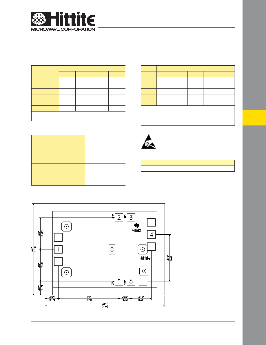
Outline Drawing
NOTES:
1. ALL DIMENSIONS ARE IN INCHES [MM]
2. DIE THICKNESS IS .004"
3. TYPICAL BOND PAD IS .004"
4. BACKSIDE METALIZATION: GOLD
5. BOND PAD METALIZATION: GOLD
6. BACKSIDE METAL IS GROUND
7. CONNECTION NOT REQUIRED FOR
UNLABELED BOND PADS.
8. OVERALL DIE SIZE �.002"
Die Packaging Information
[1]
Standard
Alternate
GP-2
[2]
[1] Refer to the "Packaging Information" section for die
packaging dimensions.
[2] For alternate packaging information contact Hittite
Microwave Corporation.
5
M
I
X
E
R
S
- C
H
I
P
5 - 174
For price, delivery, and to place orders, please contact Hittite Microwave Corporation:
20 Alpha Road, Chelmsford, MA 01824 Phone: 978-250-3343 Fax: 978-250-3373
Order On-line at www.hittite.com
HMC527
GaAs MMIC I/Q MIXER
8.5 - 13.5 GHz
v00.1204
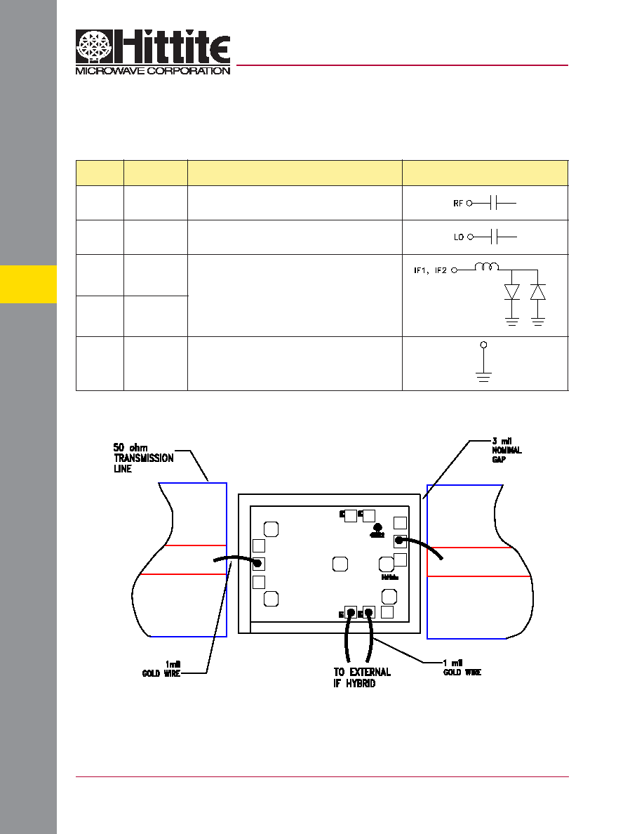
Pad
Number
Function
Description
Interface Schematic
1
RF
RF Port. This pad is AC coupled and matched to
50 Ohms from 8.5 to 13.5 GHz.
4
LO
LO Port. This pad is AC coupled and matched to
50 Ohms from 8.5 to 13.5 GHz.
2 (5)
IF2
IF Port. This pad is DC coupled. For applications not requir-
ing operation to DC, this port should be DC blocked exter-
nally using a series capacitor whose value has been chosen
to pass the necessary IF frequency range. For operation to
DC, this pad must not source/sink more than 3mA of current
or die non-function and possible die failure will result. Pads
5 and 6 are alternate IF ports.
3 (6)
IF1
GND
The backside of the die must be connected
to RF/DC ground.
Pad Descriptions
Assembly Diagrams