8
A
M
P
L
IF
IE
RS
-
S
M
T
8 - 550
For price, delivery, and to place orders, please contact Hittite Microwave Corporation:
20 Alpha Road, Chelmsford, MA 01824 Phone: 978-250-3343 Fax: 978-250-3373
Order On-line at www.hittite.com
HMC549MS8G
/
549MS8GE
General Description
Features
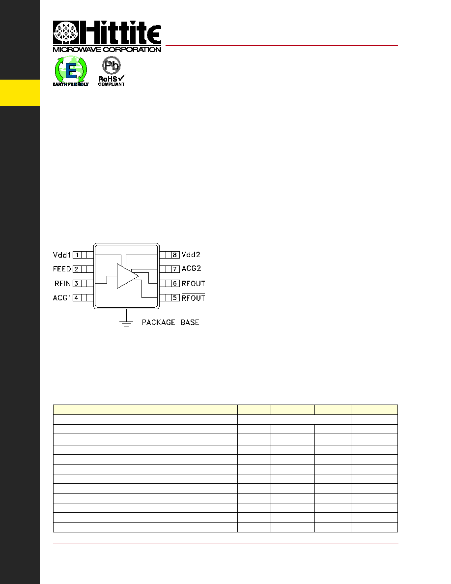
Functional Diagram
The HMC549MS8G & HMC549MS8GE are GaAs
PHEMT MMIC Low Noise Amplifi ers that are ideal
pre-amplifi ers for CATV Set Top Box, Home Gateway,
and Digital Television receivers operating between
40 and 960 MHz. This high dynamic range LNA has
been optimized to provide 3.5 dB noise fi gure and
+27 dBm output IP3 from a single supply of +5.0V @
120 mA. The outputs of this LNA are extremely well
balanced, and can be used to drive a differential input
tuner with very high input IP2 requirements. This dual
purpose LNA can also be used as an active splitter
driving two single-ended input tuners. This LNA is
housed in a RoHS compliant MSOP8G SMT package
with exposed ground paddle.
Single-ended or Balanced Output
High Output IP3: +27 dBm
Low Noise Figure: 3.5 dB
Single Positive Supply: +5V
75 Ohm Input
Electrical Specifications, 75 Ohm System,
T
A
= +25� C, Vdd = +5V
Typical Applications
The HMC549MS8G / HMC549MS8GE is ideal for:
� DTV Receivers
� Multi-Tuner Set Top Boxes
� PVRs & Home Gateways
Parameter*
Min.
Typ.
Max.
Units
Frequency Range
0.04 - 0.96
GHz
Gain
2
5
dB
Gain Variation over Temperature
0.01
0.02
dB/�C
Noise Figure
3.5
5.2
dB
Input Return Loss
8
dB
Output Return Loss
15
dB
Output Power for 1 dB Compression (P1dB)
12.5
dBm
Output Third Order Intercept (OIP3)
27
dBm
Output Second Order Intercept (OIP2)
52
dBm
Amplitude Balance
0.3
dB
Phase Balance
2
deg
Supply Current (Idd)
120
mA
* Unless otherwise noted, all measurements performed with balun on the output.
DUAL OUTPUT LOW NOISE
AMPLIFIER, 0.04 - 0.96 GHz
v01.0106
8
A
M
P
L
IF
IE
RS
-
S
M
T
8 - 551
For price, delivery, and to place orders, please contact Hittite Microwave Corporation:
20 Alpha Road, Chelmsford, MA 01824 Phone: 978-250-3343 Fax: 978-250-3373
Order On-line at www.hittite.com
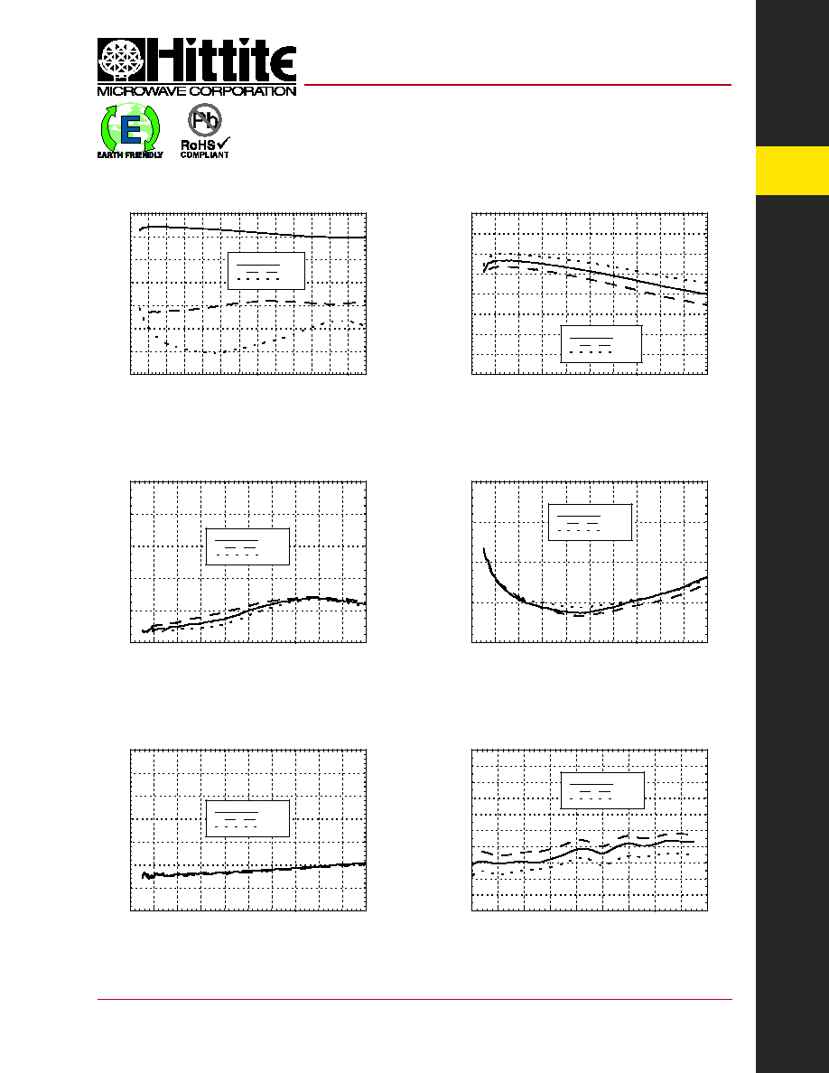
Broadband Gain & Return Loss
Gain vs. Temperature
Input Return Loss vs. Temperature
Noise Figure vs. Temperature
Output Return Loss vs. Temperature
-20
-16
-12
-8
-4
0
4
8
0
0.1 0.2 0.3 0.4 0.5 0.6 0.7 0.8 0.9
1
1.1 1.2 1.3
S21
S11
S22
RESPONSE (dB)
FREQUENCY (GHz)
HMC549MS8G
/
549MS8GE
v01.0106
Reverse Isolation vs. Temperature
-20
-15
-10
-5
0
0
0.1
0.2
0.3
0.4
0.5
0.6
0.7
0.8
0.9
1
+25 C
+85 C
-40 C
RETURN LOSS (dB)
FREQUENCY (GHz)
0
1
2
3
4
5
6
7
8
9
10
0.1
0.2
0.3
0.4
0.5
0.6
0.7
0.8
0.9
1
+25 C
+85 C
-40 C
NOI
SE FI
GURE (dB)
FREQUENCY (GHz)
-35
-30
-25
-20
-15
-10
-5
0
0
0.1
0.2
0.3
0.4
0.5
0.6
0.7
0.8
0.9
1
+25 C
+85 C
-40 C
REVERSE ISOLATION (dB)
FREQUENCY (GHz)
-10
-8
-6
-4
-2
0
0
0.1
0.2
0.3
0.4
0.5
0.6
0.7
0.8
0.9
1
+25 C
+85 C
-40 C
RETURN LOSS (dB)
FREQUENCY (GHz)
0
1
2
3
4
5
6
7
8
0
0.1
0.2
0.3
0.4
0.5
0.6
0.7
0.8
0.9
1
+25C
+85C
- 40C
GAIN
(dB)
FREQUENCY (GHz)
All measurements taken in 75 Ohm system.
DUAL OUTPUT LOW NOISE
AMPLIFIER, 0.04 - 0.96 GHz

8
A
M
P
L
IF
IE
RS
-
S
M
T
8 - 552
For price, delivery, and to place orders, please contact Hittite Microwave Corporation:
20 Alpha Road, Chelmsford, MA 01824 Phone: 978-250-3343 Fax: 978-250-3373
Order On-line at www.hittite.com
Psat vs. Temperature
P1dB vs. Temperature
Output IP3 vs. Temperature
Gain, Noise Figure & P1dB vs.
Supply Voltage @ 500 MHz
HMC549MS8G
/
549MS8GE
v01.0106
Phase Balance *
Amplitude Balance *
8
9
10
11
12
13
14
15
0.1
0.2
0.3
0.4
0.5
0.6
0.7
0.8
0.9
1
+25 C
+85 C
-40 C
P1dB (dBm)
FREQUENCY (GHz)
0
2
4
6
8
10
5
7
9
11
13
15
3
3.5
4
4.5
5
5.5
GAIN
NOISE FIGURE
P1dB
GAIN & NOISE FIGURE (dB)
P1dB (dBm)
SUPPLY VOLTAGE (Vdc)
-6
-4
-2
0
2
4
6
8
10
0
0.1
0.2
0.3
0.4
0.5
0.6
0.7
0.8
0.9
1
PHASE ERROR (deg)
FREQUENCY (GHz)
-0.5
-0.4
-0.3
-0.2
-0.1
0
0
0.1
0.2
0.3
0.4
0.5
0.6
0.7
0.8
0.9
1
AMPLITUDE ERROR (dB)
FREQUENCY (GHz)
20
21
22
23
24
25
26
27
28
29
30
31
32
0.1
0.2
0.3
0.4
0.5
0.6
0.7
0.8
0.9
1
+25 C
+85 C
-40 C
OUTPUT IP3 (dBm)
FREQUENCY (GHz)
8
9
10
11
12
13
14
15
16
17
0.1
0.2
0.3
0.4
0.5
0.6
0.7
0.8
0.9
1
+25 C
+85 C
-40 C
Psat (dBm)
FREQUENCY (GHz)
* Data taken without balun on the output.
All measurements taken in 75 Ohm system.
DUAL OUTPUT LOW NOISE
AMPLIFIER, 0.04 - 0.96 GHz
8
A
M
P
L
IF
IE
RS
-
S
M
T
8 - 553
For price, delivery, and to place orders, please contact Hittite Microwave Corporation:
20 Alpha Road, Chelmsford, MA 01824 Phone: 978-250-3343 Fax: 978-250-3373
Order On-line at www.hittite.com
Absolute Maximum Ratings
Drain Bias Voltage (Vdd)
+7.0 Vdc
RF Input Power (RFin)(Vdd = +3.0 Vdc)
0 dBm
Channel Temperature
150 �C
Continuous Pdiss (T = 85 �C)
(derate 20 mW/�C above 85 �C)
1.32 W
Thermal Resistance
(channel to ground paddle)
49 �C/W
Storage Temperature
-65 to +150 �C
Operating Temperature
-40 to +85 �C
ESD Sensitivity (HBM)
Class 1A
ELECTROSTATIC SENSITIVE DEVICE
OBSERVE HANDLING PRECAUTIONS
HMC549MS8G
/
549MS8GE
v01.0106
Vdd (Vdc)
Idd (mA)
3.0
117.1
3.3
117.5
3.6
117.9
4.5
118.5
5.0
119.0
5.5
119.3
Typical Supply Current vs. Vdd
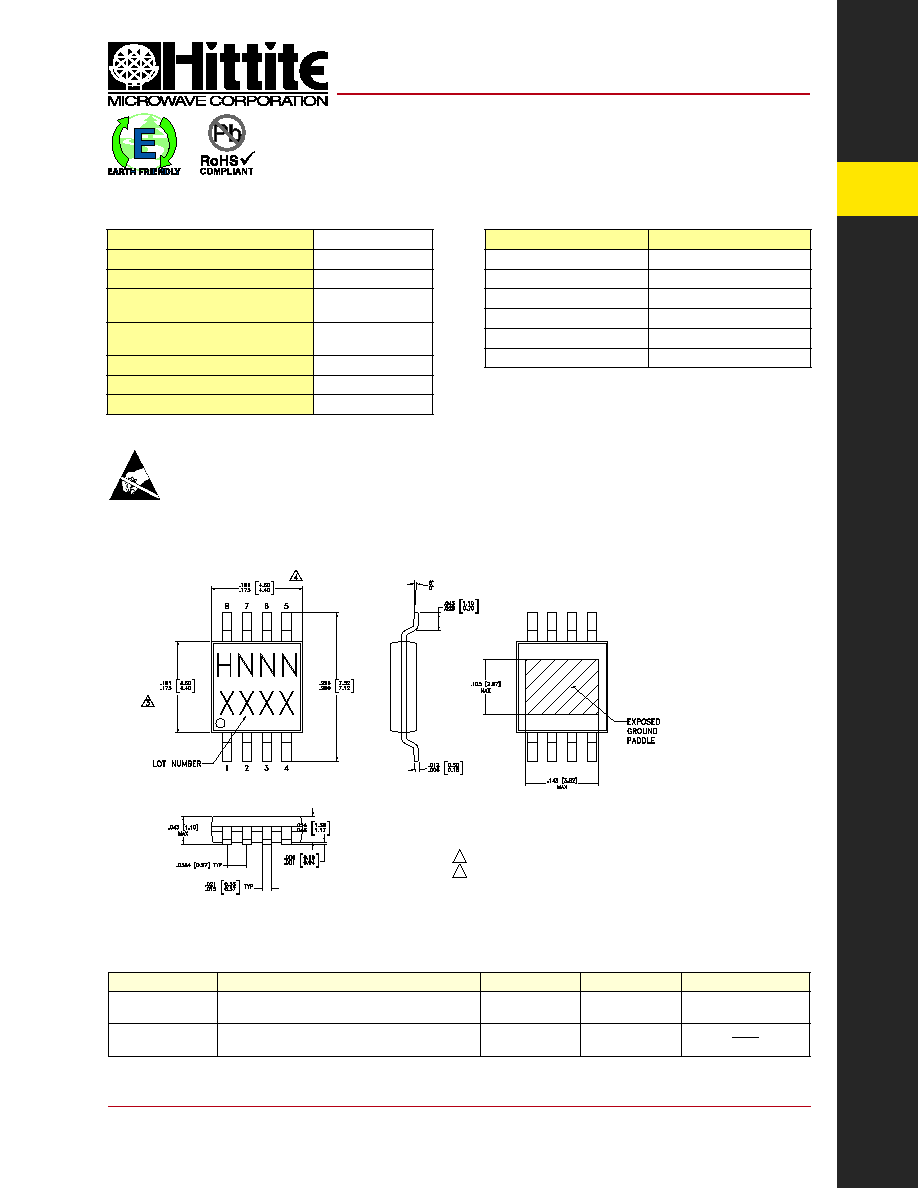
Outline Drawing
Part Number
Package Body Material
Lead Finish
MSL Rating
Package Marking
[3]
HMC549MS8G
Low Stress Injection Molded Plastic
Sn/Pb Solder
MSL1
[1]
H549
XXXX
HMC549MS8GE
RoHS-compliant Low Stress Injection Molded Plastic
100% matte Sn
MSL1
[2]
H549
XXXX
[1] Max peak refl ow temperature of 235 �C
[2] Max peak refl ow temperature of 260 �C
[3] 4-Digit lot number XXXX
Package Information
NOTES:
1. LEADFRAME MATERIAL: COPPER ALLOY
2. DIMENSIONS ARE IN INCHES [MILLIMETERS].
3. DIMENSION DOES NOT INCLUDE MOLDFLASH OF 0.15mm PER SIDE.
4. DIMENSION DOES NOT INCLUDE MOLDFLASH OF 0.25mm PER SIDE.
5. ALL GROUND LEADS AND GROUND PADDLE MUST BE SOLDERED TO
PCB RF GROUND.
DUAL OUTPUT LOW NOISE
AMPLIFIER, 0.04 - 0.96 GHz

8
A
M
P
L
IF
IE
RS
-
S
M
T
8 - 554
For price, delivery, and to place orders, please contact Hittite Microwave Corporation:
20 Alpha Road, Chelmsford, MA 01824 Phone: 978-250-3343 Fax: 978-250-3373
Order On-line at www.hittite.com
HMC549MS8G
/
549MS8GE
v01.0106
Pin Descriptions
Pin Number
Function
Description
Interface Schematic
1, 8
Vdd1, Vdd2
Power supply voltage for the fi rst stage. An external choke
inductor is required. See application circuit.
2
FEED
Feedback capacitor for the fi rst stage.
3
RFIN
This pin is DC coupled and requires a DC blocking cap.
See application circuit.
4
ACG1
This pin has to be terminated by an external capacitor.
See application circuit.
5
RFOUT
RF differential output 2. This port is DC coupled.
6
RFOUT
RF differential output 1. This port is DC coupled.
7
ACG2
This pin has to be terminated by an external capacitor.
See application circuit.
8
Vdd2
Power supply voltage for second stage. An external choke
inductor is required. See application circuit.
DUAL OUTPUT LOW NOISE
AMPLIFIER, 0.04 - 0.96 GHz