 | –≠–ª–µ–∫—Ç—Ä–æ–Ω–Ω—ã–π –∫–æ–º–ø–æ–Ω–µ–Ω—Ç: HT1381 | –°–∫–∞—á–∞—Ç—å:  PDF PDF  ZIP ZIP |
Document Outline
- ˛ˇ
- ˛ˇ
- ˛ˇ
- ˛ˇ
- ˛ˇ
- ˛ˇ
- ˛ˇ
- ˛ˇ
- ˛ˇ
- ˛ˇ
- ˛ˇ
- ˛ˇ
- ˛ˇ
- ˛ˇ
HT1380/HT1381
Serial Timekeeper Chip
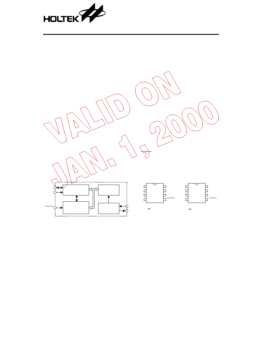
Block Diagram
Pin Assignment
1
October 2, 1999
Features
∑
Operating voltage: 2.0V~5.5V
∑
Maximum input serial clock: 500kHz at
V
DD
=2V, 2MHz at V
DD
=5V
∑
Operating current: less than 400nA at 2V,
less than 1.2mA at 5V
∑
TTL compatible
-
V
IH
: 2.0V~V
DD
+0.3V at V
DD
=5V
-
V
IL
: -0.3V~+0.8V at V
DD
=5V
∑
Two data transmission modes: single-byte,
or burst mode
∑
Serial I/O transmission
∑
All registers store BCD format
∑
HT1380: 8-pin DIP package
HT1381: 8-pin SOP package
General Description
The HT1380/HT1381 is a serial timekeeper IC
which provides seconds, minutes, hours, day,
date, month and year information. The number
of days in each month and leap years are auto-
matically adjusted. The HT1380/HT1381 is de-
signed for low power consumption and can
operate in two modes: one is the 12-hour mode
with an AM/PM indicator, the other is the
24-hour mode.
The HT1380/HT1381 has several registers to
store the corresponding information with 8-bit
data format. A 32768Hz crystal is required to
provide the correct timing. In order to minimize
the pin number, the HT1380/HT1381 use a se-
rial I/O transmission method to interface with a
microprocessor. Only three wires are required:
(1) REST, (2) SCLK and (3) I/O. Data can be de-
livered 1 byte at a time or in a burst of up to 8
bytes.
Applications
∑
Microcomputer serial clock
∑
Clock and Calendar
1
2
3
4
8
7
6
5
N C
X 1
X 2
V S S
V D D
S C L K
I / O
R E S T
H T 1 3 8 0
8 D I P
1
2
3
4
8
7
6
5
N C
X 1
X 2
V S S
V D D
S C L K
I / O
R E S T
H T 1 3 8 1
8 S O P
R E S T
D a t a S h i f t
R e g i s t e r
C o m m a n d
C o n t r o l L o g i c
R e a l T i m e
C l o c k
O s c i l l a t o r a n d
D i v i d e r
C i r c u i t
X 1
X 2
S C L K
I / O

Pad Assignment
Pad Coordinates
Unit: mm
Pad No.
X
Y
1
-851.40
775.00
2
-851.40
494.60
3
-844.40
-203.90
4
845.90
-618.30
5
848.40
-4.30
6
845.90
332.60
7
844.40
572.60
Chip size: 2010 ¥ 1920 (mm)
2
* The IC substrate should be connected to VSS in the PCB layout artwork.
Pad Description
Pad No. Pad Name I/O
Internal
Connection
Description
1
X1
I
CMOS
32768Hz crystal input pad
2
X2
O
CMOS
Oscillator output pad
3
VSS
I
CMOS
Ground pin
4
REST
I
CMOS
Reset pin with serial transmission
5
I/O
I/O
CMOS
Data input/output pin with serial transmission
6
SCLK
I
CMOS
Serial clock pulse pin with serial transmission
7
VDD
I
CMOS
Power supply pin
Absolute Maximum Ratings
Supply Voltage..............................-0.3V to 5.5V
Storage Temperature.................-50∞C to 125∞C
Input Voltage.................V
SS
-0.3V to V
DD
+0.3V
Operating Temperature ..................0∞C to 70∞C
Note: These are stress ratings only. Stresses exceeding the range specified under ≤Absolute Maxi-
mum Ratings≤ may cause substantial damage to the device. Functional operation of this de-
vice at other conditions beyond those listed in the specification is not implied and prolonged
exposure to extreme conditions may affect device reliability.
HT1380/HT1381
2
October 2, 1999
1
2
3
4
5
6
7
( 0 , 0 )
X 1
X 2
V S S
I / O
S C L K
V D D
R E S T

D.C. Characteristics
Ta=25∞C
Symbol
Parameter
Test Conditions
Min.
Typ.
Max.
Unit
V
DD
Conditions
V
DD
Operating Voltage
æ
æ
2
æ
5.5
V
I
STB
Standby Current
2V
æ
æ
æ
100
nA
5V
æ
æ
100
nA
I
DD
Operating Current
2V
No load
æ
0.7
1.0
mA
5V
æ
0.7
1.2
mA
I
OH
Source Current
2V
V
OH
=1.8V
-0.2
-0.4
æ
mA
5V
V
OH
=4.5V
-0.5
-1.0
æ
mA
I
OL
Sink Current
2V
V
OL
=0.2V
0.7
1.5
æ
mA
5V
V
OL
=0.5V
2.0
4.0
æ
mA
V
IH
≤H≤ Input Voltage
5V
æ
2
æ
æ
V
V
IL
≤L≤ Input Voltage
5V
æ
æ
æ
0.8
V
f
OSC
System Frequency
5V
32768Hz X¢TAL
æ
32768
æ
Hz
f
SCLK
Serial Clock
2V
æ
æ
æ
0.5
MHz
5V
æ
æ
2
MHz
* I
STB
is specified with SCLK, I/O, REST open. The clock halt bit must be set to logic 1 (oscillator
disabled).
A.C. Characteristics
Ta=25∞C
Symbol
Parameter
Test Conditions
Min.
Max.
Unit
V
DD
Conditions
t
DC
Data to Clock Setup
2V
æ
200
æ
ns
5V
æ
50
æ
t
CDH
Clock to Data Hold
2V
æ
280
æ
ns
5V
æ
70
æ
t
CDD
Clock to Data Delay
2V
æ
æ
800
ns
5V
æ
æ
200
t
CL
Clock Low Time
2V
æ
1000
æ
ns
5V
æ
250
æ
t
CH
Clock High Time
2V
æ
1000
æ
ns
5V
æ
250
æ
f
CLK
Clock Frequency
2V
æ
æ
0.5
MHz
5V
æ
D.C.
2.0
HT1380/HT1381
3
October 2, 1999

Symbol
Parameter
Test Conditions
Min.
Max.
Unit
V
DD
Conditions
t
r
Clock Rise and Fall Time
2V
æ
æ
2000
ns
t
f
5V
æ
æ
500
t
CC
Reset to Clock Setup
2V
æ
4
æ
us
5V
æ
1
æ
t
CCH
Clock to Reset Hold
2V
æ
240
æ
ns
5V
æ
60
æ
t
CWH
Reset Inactive Time
2V
æ
4
æ
us
5V
æ
1
æ
t
CDZ
Reset to I/O High Impedance
2V
æ
æ
280
ns
5V
æ
æ
70
HT1380/HT1381
4
October 2, 1999
Functional Description
The HT1380/HT1381 mainly contains the fol-
lowing internal elements: a data shift register
array to store the clock/calendar data, com-
mand control logic, oscillator circuit and read
timer clock. The clock is contained in eight
read/write registers as shown below. Data con-
tained in the clock register is in binary coded
decimal format.
Two modes are available for transferring the
data between the microprocessor and the
HT1380/HT1381. One is in single-byte mode ad
the other is in multiple-byte mode.
The HT1380/HT1381 also contains two addi-
tional bits, the clock halt bit (CH) and the write
protect bit (WP). These bits control the opera-
tion of the oscillator and so data can be written
to the register array. These two bits should first
be specified in order to read from and write to
the register array properly.
Command byte
For each data transfer, a Command Byte is initiated to specify which register is accessed. This is to
determine whether a read, write, or test cycle is operated and whether a single byte or burst mode
transfer is to occur. Refer to the table shown below and follow the steps to write the data to the chip.
First give a Command Byte of HT1380/HT1381, and then write a data in the register.
This table illustrates the correlation between Command Byte and their bits:
Command Byte
Function Description
C7
C6
C5
C4
C3
C2
C1
C0
Select Read or Write Cycle
R/W
Specify the Register to be Accessed
A2
A1
A0
Clock Halt Flag
C
For IC Test Only
1
0
0
1
x
x
x
1
Select Single Byte or Burst Mode
1
0
1
1
1
1
1
x
Note: ≤x≤ stands for don¢t care

HT1380/HT1381
5
October 2, 1999
The following table shows the register address and its data format:
Register
Name
Range
Data
Register Definition
Address
A2~A0
Bit
R/W
Command
Byte
D7 D6 D5 D4 D3 D2 D1 D0
Seconds
00~59
CH
10 SEC
SEC
000
W
R
10000000
10000001
Minutes
00~59
0
10 MIN
MIN
001
W
R
10000010
10000011
Hours
01~12
00~23
12\
24
0
0
AP
10
HR
HR
HOUR
010
W
R
10000100
10000101
Date
01~31
0
0 10 DATE
DATE
011
W
R
10000110
10000111
Month
01~12
0
0
0 10M
MONTH
100
W
R
10001000
10001001
Day
01~07
0
0
0
0
DAY
101
W
R
10001010
10001011
Year
00~99
10 YEAR
YEAR
110
W
R
10001100
10001101
Write
Protect
00~80
WP
ALWAYS ZERO
111
W
R
10001110
10001111
CH:
WP:
Clock Halt bit
CH=0 oscillator enabled
CH=1 oscillator disabled
Write protect bit
WP=0 register data can be written in
WP=1 register data can not be written in
Bit 7 of Reg2:
Bit 5 of Reg2:
12/24 mode flag
bit 7=1, 12-hour mode
bit 7=0, 24-hour mode
AM/PM mode defined
AP=1 PM mode
AP=0 AM mode
R/W signal
The LSB of the Command Byte determines
whether the data in the register be read or be
written to.
When it is set as ≤0≤ means that a write cycle is
to take place otherwise this chip will be set into
the read mode.
A0~A2
A0 to A2 of the Command Byte is used to specify
which registers are to be accessed. There are
eight registers used to control the month data,
etc., and each of these registers have to be set as
a write cycle in the initial time.
Burst mode
When the Command Byte is 10111110 (or
10111111), the HT1380/HT1381 is configured in
burst mode. In this mode the eight clock/calen-
dar registers can be written (or read) in series,
starting with bit 0 of register address 0 (see the
timing on the next page).
Test mode
When the Command Byte is set as 1001xxx1,
HT1380/HT1381 is configured in test mode.
The test mode is used by Holtek only for testing
purposes. If used generally, unpredictable con-
ditions may occur.