 | –≠–ª–µ–∫—Ç—Ä–æ–Ω–Ω—ã–π –∫–æ–º–ø–æ–Ω–µ–Ω—Ç: HT1609 | –°–∫–∞—á–∞—Ç—å:  PDF PDF  ZIP ZIP |
HT1609L
2
◊
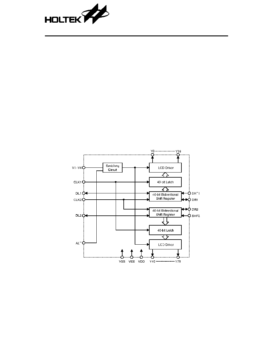
40 Channel LCD Driver
Block Diagram
Features
∑
Operating voltage: 2.7V~5.2V
∑
Bias voltage: static~1/5 bias
∑
LCD driving voltage: 3.0V~5.0V
∑
2
◊
40 internal LCD drivers available
∑
LCD driver with serial/parallel conversion
function
General Description
The HT1609L is an LCD driver LSI with 2
◊
40
output channels using CMOS technology. It is
equipped with two sets of 40-bit bidirectional
shift registers, 40-bit data latches, 40-bit LCD
drivers, and logic control circuits.
The HT1609L can convert serial data received
from an LCD controller into parallel data and
send out LCD driving waveforms to the LCD
panel. The HT1609L is designed for general
purpose LCD drivers. It can drive both static
and dynamic drive LCDs. The LSI can be used
as segment driver.
Applications
∑
Electronic dictionaries
∑
Portable computers
∑
Remote controllers
∑
Calculators
1
25th Aug '98

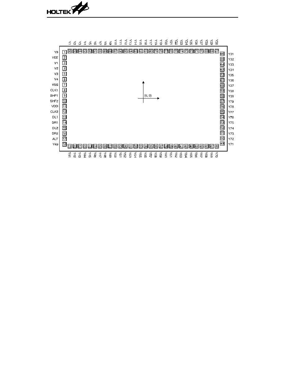
Pin Assignment
HT1609L
2
25th Aug '98
Pad Assignment
Chip size: 162
◊
102 (mil)
2
* The IC substrate should be connected to VDD in the PCB layout artwork.
HT1609L
3
25th Aug '98
Pad Coordinates
Unit: mil
Pad No.
X
Y
Pad No.
X
Y
1
≠75.27
44.20
49
75.22
≠43.31
2
≠75.27
39.01
50
75.22
≠38.25
3
≠75.27
33.83
51
75.22
≠33.19
4
≠75.27
28.65
52
75.22
≠28.14
5
≠75.27
23.46
53
75.22
≠23.08
6
≠75.27
18.27
54
75.22
≠18.02
7
≠75.27
13.09
55
75.22
≠12.96
8
≠75.27
7.91
56
75.22
≠7.91
9
≠75.27
2.63
57
75.22
≠2.85
10
≠75.27
≠2.55
58
75.22
2.21
11
≠75.27
≠7.61
59
75.22
7.27
12
≠75.27
≠12.66
60
75.22
12.32
13
≠75.27
≠17.85
61
75.22
17.38
14
≠75.27
≠23.12
62
75.22
22.44
15
≠75.27
≠28.31
63
75.22
27.50
16
≠75.27
≠33.58
64
75.22
32.56
17
≠75.27
≠38.76
65
75.22
37.61
18
≠75.27
≠43.99
66
75.22
42.67
19
≠70.34
≠45.73
67
70.17
45.13
20
≠65.49
≠45.73
68
65.32
45.13
21
≠60.65
≠45.73
69
60.48
45.13
22
≠55.80
≠45.73
70
55.63
45.13
23
≠50.96
≠45.73
71
50.79
45.13
24
≠46.11
≠45.73
72
45.94
45.13
25
≠41.27
≠45.73
73
41.10
45.13
26
≠36.42
≠45.73
74
36.25
45.13
27
≠31.58
≠45.73
75
31.41
45.13
28
≠26.73
≠45.73
76
26.56
45.13
29
≠21.89
≠45.73
77
21.72
45.13
30
≠17.04
≠45.73
78
16.87
45.13
31
≠12.20
≠45.73
79
12.03
45.13
32
≠7.35
≠45.73
80
7.18
45.13
33
≠2.51
≠45.73
81
2.34
45.13
34
2.34
≠45.73
82
≠2.51
45.13
35
7.18
≠45.73
83
≠7.35
45.13
36
12.03
≠45.73
84
≠12.20
45.13
37
16.87
≠45.73
85
≠17.04
45.13
38
21.72
≠45.73
86
≠21.89
45.13
39
26.56
≠45.73
87
≠26.73
45.13
40
31.41
≠45.73
88
≠31.58
45.13
41
36.25
≠45.73
89
≠36.42
45.13
42
41.10
≠45.73
90
≠41.27
45.13
43
45.94
≠45.73
91
≠46.11
45.13
44
50.79
≠45.73
92
≠50.96
45.13
45
55.63
≠45.73
93
≠55.80
45.13
46
60.48
≠45.73
94
≠60.65
45.13
47
65.32
≠45.73
95
≠65.49
45.13
48
70.17
≠45.73
96
≠70.34
45.13
HT1609L
4
25th Aug '98

Pad Description
Pad No.
Pad Name I/O
Description
1
Y0
O
LCD driver output for channel 1
2
VEE
--
LCD power supply
3~6
V1~V4
I
LCD bias supply voltage for LCD driver
7
VSS
--
Power supply (ground)
8
CLK1
I
Clock to latch serial data on the falling edge (Note 1)
9
SHF1
I
Shift direction selection of channel 1 shift register (Note 2)
10
SHF2
I
Shift direction selection of channel 2 shift register (Note 2)
11
VDD
--
Power supply ( positive )
12
CLK2
I
Clock to shift serial data on the falling edge (Note 1)
13
DL1
I/O Data input/output of channel 1 shift register
14
DR1
I/O Data input/output of channel 1 shift register
15
DL2
I/O Data input/output of channel 2 shift register
16
DR2
I/O Data input/output of channel 2 shift register
17
ALT
I
Alternate signal input for LCD driving waveform
18~57
Y40~Y79
O
LCD driver outputs for channel 2
58~96
Y39~Y1
O
LCD driver outputs for channel 1
Note 1: Data is processed on the clock falling or rising edge as shown in the following table.
HT1609L
5
25th Aug '98
The output levels of channel 1 and 2 are decided by the combination of ALT
and latched data. Refer to the following table:
Latched Data
ALT
Channel 1
(Y0~Y39)
Channel 2
(Y40~Y79)
H
(Selected)
H
V1
V1
L
V2
V2
L
(Non-selected)
H
V3
V3
L
V4
V4
Note 2 : Shift direction of channel 1 and 2
Shift Direction of Channel 1 (Channel 2)
SHF1 (SHF2)
Shift Direction
DL1 (DL2)
DR1 (DR2)
H
Y39 to Y0 (Y79 to Y40)
OUT
IN
L
Y0 to Y39 (Y40 to Y79)
IN
OUT
Absolute Maximum Ratings*
Supply Voltage .............................. ≠0.3V to 5.5V
Storage Temperature................. ≠50
∞
C to 125
∞
C
Input Voltage..................V
SS
≠0.3V to V
DD
+0.3V
Operating Temperature............... ≠20
∞
C to 70
∞
C
*Note: These are stress ratings only. Stresses exceeding the range specified under "Absolute Maxi-
mum Ratings" may cause substantial damage to the device. Functional operation of this
device at other conditions beyond those listed in the specification is not implied and prolonged
exposure to extreme conditions may affect device reliability.
HT1609L
6
25th Aug '98
D.C. Characteristics
Ta=25
∞
C
Symbol
Parameter
Test Conditions
Min.
Typ.
Max.
Unit
V
DD
Conditions
V
DD
Operating Voltage
--
--
2.7
--
5.2
V
I
DD
Operating Current
5V
No load
--
100
300
µ
A
I
STB
Standby Current
5V
--
--
1
5
µ
A
V
IL
"L" Input Voltage
5V
--
--
--
1
V
V
IH
"H" Input Voltage
5V
--
4
--
--
V
V
OL
"L" Output Voltage
5V
I
OL
=+0.4mA
--
--
0.4
V
V
OH
"H" Output Voltage
5V
I
OH
=≠0.4mA
4.6
--
--
V
V
LCD
LCD Driving Voltage
--
V
DD
≠V
EE
3
--
5.0
V
A.C. Characteristics
Ta=25
∞
C
Symbol
Parameter
Test Conditions
Min.
Typ.
Max.
Unit
V
DD
Conditions
f
CLK2
Data Shift Frequency
5V
--
--
--
400
kHz
t
WCKH
Clock High Level Width
5V
--
800
--
--
ns
t
WCKL
Clock Low Level Width
5V
--
800
--
--
ns
t
SU
Data Setup Time
5V
--
300
--
--
ns
t
DH
Data Hold Time
5V
--
300
--
--
ns
t
DD
Data Delay Time
5V
--
--
--
500
ns
t
SUC1
Clock Setup Time
5V
CLK2
CLK1
500
--
--
ns
t
SUC2
Clock Setup Time
5V
CLK1
CLK 2
500
--
--
ns
t
R
/t
F
Clock Rise/Fall Time
5V
--
--
--
200
ns
HT1609L
7
25th Aug '98

Functional Description
The HT1609L is an LCD driver LSI with 2
◊
40
segment output channel. It operates with a con-
troller, such as HT163A, or another segment
driver LSI HT1608, HT1608L and HT1609L.
Clock
The CLK1 is the clock to latch data on the
falling edge. It latches the data input from the
bidirectional shift register at the falling edge of
CLK1 and transfers its outputs to the LCD
driver circuit. The CLK2 is the clock to shift
data on the falling edge. It shifts the serial data
at the falling of CLK2 and transfers the output
of each bit of the register to the latch circuit
(refer to Note 1).
Bidirectional shift register
The HT1609L supplies two sets of 40-bit shift
register, which controls the shift direction by
SHF1 & SHF2. The SHF1 controls the 1st 40-
bit shift register, and SHF2 controls the 2nd
40-bit shift register. When SHF1 is connected to
VDD, the 1st shift direction is from Y39 to Y0;
when SHF1 is connected to VSS, the shift direc-
tion changes from Y0 to Y39. When SHF2 is
connected to VDD, the 2nd shift direction is
from Y79 to Y40; when SHF2 is connected to
VSS, the shift direction changes from Y40 to
Y79 (refer to Note 2).
Data input/output
The DL1, DR1, DL2, DR2 are data input or
output option function. When SHF1 (SHF2) is
connected to VDD, the 40th bit data of the 1st
(2nd) 40-bit shift register outputs from DL1
(DL2) ; when SHF1 (SHF2) is connected to VSS
or open , the 1~40 (41~80) bits data from LCD
controller enter into the 1st (2nd) 40-bit shift
through DL1 (DL2).
When SHF1 (SHF2) is connected to VDD, the
1~40 (41~80) bit data from the LCD controller
enter into the 1st (2nd)40-bit shift register
through DR1 (DR2); when SHF1 (SHF2) is con-
nected to VSS or open , the 40th bit shift regis-
ter outputs from DR1 (DR2) (refer to Note 2).
LCD driver circuit
Select one of the four levels of voltage V1, V2,
V3,and V4 for driving an LCD and transfer it to
the output terminals according to the combina-
tion of alternate signal (ALT) and the data in
the latch circuit (refer to Note 1).
HT1609L
8
25th Aug '98
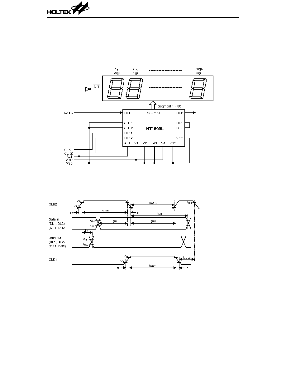
Timing Diagrams
Static driver
When the HT1609L is used as a static driver,
data is transferred on the falling edge of CLK2
and latched on the falling edge of CLK1. The
frequency of CLK1 becomes the frame fre-
quency of the LCD driver. The frequency of ALT
has to be twice the frequency of CLK1. ALT has
to be synchronized on the falling edge of CLK1.
The power supply for the LCD driver is used by
shortening V1, V4 or V2, V3. The application
circuit connections are shown below:
HT1609L
9
25th Aug '98

Application Circuits
HT1609L
10
25th Aug '98