 | –≠–ª–µ–∫—Ç—Ä–æ–Ω–Ω—ã–π –∫–æ–º–ø–æ–Ω–µ–Ω—Ç: HT1613C | –°–∫–∞—á–∞—Ç—å:  PDF PDF  ZIP ZIP |
Document Outline
- ˛ˇ
- ˛ˇ
- ˛ˇ
- ˛ˇ
- ˛ˇ
- ˛ˇ
- ˛ˇ
- ˛ˇ
- ˛ˇ
- ˛ˇ
- ˛ˇ
- ˛ˇ

HT1613C
Timer with Dialer Interface
Block Diagram
Rev. 1.10
1
August 17, 2001
Features
∑
Operating voltage: 1.2V~1.7V
∑
Low operating current: 3mA (typ.)
∑
Dialing number and conversation time display
∑
Conversation timer (59 mins and 59 secs max.)
∑
8 or 10-digit LCD display driver; 3V, 1/2 bias, 1/3 duty (8
digit hand-held calculator LCD used for 8-digit applica-
tion)
∑
Real time clock with stopwatch
∑
Built-in dialer interface
∑
12-hour or 24-hour format
∑
Uses 32768Hz crystal
∑
Two-button sequential operation for real time clock
setting
∑
Pad options
-
Real time (RT)
-
Auto change to timer mode (ACT)
-
Extension phone number display (EPN)
∑
Blinking cursor waits for dialing number
∑
Last call time display
General Description
The HT1613C is a CMOS chip designed for dialer inter-
faces driving 8 or 10 digit LCDs. Various functions, such
as real time clock, dialing number and conversation time
display are provided.
The HT1613C can display the real time or be blank by
default. When answering a telephone call, the timer is
activated to tell users how long the conversation has
taken. The HT1613C receives dialing data from the di-
aler and displays the phone number on the LCD from left
to right each time a phone call is made. By adding a
TIMER key, the HT1613C can provide the stopwatch
and timer reset/hold functions. Refer to the functional
description for details.
Applications
∑
Timers, clocks and watches
∑
LCD display drivers
∑
Telephone display interface
∑
Instrument display
Patent Number: 84545 (R.O.C.)
Patent Pending: 08/214, 079 (U.S.A.)
T 1
E P N
S K
S E G 1
S E G 3 0
T I M E R
S 1
H K
T i m e
B a s e
T i m e r
S h i f t
R e g i s t e r
S t a t e
C o n t r o l
C o n t r o l
C i r c u i t
C o m m o n
C i r c u i t
D e c o d e r
&
M U X
V o l t a g e
D o u b l e r
S e g m e n t
L a t c h
&
S e l e c t
S c a n
C K T
X 1
X 2
S 2
I N T
C O M 1
C O M 2
C O M 3
V A
V B
V C
R T
A C T
R E S
1 2 / 2 4
D I
T 2

Pad Assignment
Chip size: 128 ¥ 141 (mil)
2
* The IC substrate should be connected to VDD in the PCB layout artwork.
Pad Coordinates
Unit: mil
Pad No.
X
Y
Pad No.
X
Y
Pad No.
X
Y
1
-57.91
45.52
19
-10.25
-61.96
37
58.10
28.84
2
-57.91
38.59
20
2.76
-61.96
38
58.10
36.19
3
-57.91
31.67
21
11.94
-62.50
39
58.10
43.53
4
-57.91
24.79
22
32.97
-62.50
40
58.10
50.87
5
-57.37
16.98
23
39.86
-62.50
41
58.10
58.22
6
-57.37
2.91
24
46.74
-62.50
42
37.26
63.04
7
-57.91
-8.60
25
58.10
-62.46
43
29.91
63.04
8
-57.91
-15.53
26
58.10
-55.04
44
22.57
63.04
9
-57.91
-22.49
27
58.10
-48.16
45
15.23
63.04
10
-57.91
-29.38
28
58.10
-36.30
46
7.88
63.04
11
-57.91
-36.26
29
58.10
-28.95
47
0.54
63.04
12
-57.91
-45.82
30
58.10
-21.61
48
-6.81
63.04
13
-57.91
-54.20
31
58.10
-15.22
49
-14.15
63.04
14
-57.91
-62.50
32
58.10
-7.88
50
-21.50
63.04
15
-47.20
-62.50
33
58.10
-0.54
51
-28.84
63.04
16
-33.43
-62.50
34
58.10
6.81
52
-36.18
63.04
17
-22.80
-62.46
35
58.10
14.15
53
-43.53
63.04
18
-16.37
-62.50
36
58.10
21.50
54
-50.87
63.04
HT1613C
Rev. 1.10
2
August 17, 2001
AC
T
1
2 8
2
2 9
3
3 0
4
3 1
5
3 2
6
3 3
7
3 4
8
3 5
9
3 6
1 0
3 7
1 1
3 8
1 2
3 9
1 3
4 0
1 4
4 1
1 5
4 2
1 6
4 3
1 7
4 4
1 8
4 5
1 9
4 6
2 0
4 7
2 1
4 8
2 2
4 9
2 3
5 0
2 4
5 1
2 5
5 2
2 6
5 3
2 7
5 4
( 0 , 0 )
SE
G
1
5
SE
G
1
6
SE
G
1
7
SE
G
1
8
SE
G
1
9
SE
G
2
0
SE
G
2
1
SE
G
2
2
SE
G
2
3
SE
G
2
4
SE
G
2
5
SE
G
2
6
SE
G
2
7
R T
S E G 1 4
S E G 1 3
S E G 1 2
S E G 1 1
S E G 1 0
S E G 9
S E G 8
S E G 7
S E G 6
S E G 5
S E G 4
S E G 3
S E G 2
S E G 1
C O M 3
C O M 1
1 2 / 2 4
S E G 2 8
S E G 2 9
S E G 3 0
C O M 2
S 2
X 2
X 1
T I M E R
S 1
H K
I N T
T 1
T 2
SK
VS
S
VA
VB
VC
VDD
DI
RE
S
EP
N

Pad Description
Pad Name
I/O
Internal
Connection
Description
SEG1~SEG30
O
CMOS OUT
LCD segment signal output pads
COM1~COM3
O
CMOS OUT
LCD common signal output pads
HK
I
CMOS IN
Pull-high
Hook switch detector input
Active low
X1
I
OSCILLATOR
32768Hz crystal oscillator input
X2
O
32768Hz crystal oscillator output
T1
I
CMOS IN
Pull-high
Test pad (connected to VSS for production test)
T2
I
CMOS IN
Pull-high
Test pad (connected to VSS for production test)
INT
O
NMOS OUT
Interrupt output, 8Hz or 16Hz by mask option
TIMER
I
CMOS IN
Pull-low
Timer reset and start/hold toggle control input pad
12/24
I
CMOS IN
Pull-low
12-hour or 24-hour format option pad, connected to VDD for 12-hour format
S1
I
CMOS IN
Pull-low
Clock setting switch
Active high
S2
I
CMOS IN
Pull-low
Clock adjusting switch
Active high
DI
I
CMOS IN
Pull-high
Serial data input pad (connected to the dialer)
Data should be valid at the falling edge of SK
SK
I
CMOS IN
Pull-high
Clock input pad (connected to the dialer)
RES
I
CMOS IN
Pull-high
System initialization pin (active low)
The pull-high resistance is 200kW typ.
RT
I
CMOS
LATCH IN
Pull-low
Real time selection pin
VDD: With real time mode
Floating: Without real time mode
EPN
I
CMOS
LATCH IN
Pull-high
Extension phone number display selection pin
VSS: Without extension phone number display
Floating: With extension phone number display
ACT
I
CMOS
LATCH IN
Pull-high
In the dialing number display mode, auto change to timer mode selection
VSS: Auto change to timer mode
Floating: Manual change to timer mode
VA
O
CMOS OUT
Voltage doubler, connected to external capacitor
VB
O
CMOS OUT
Voltage doubler, connected to external capacitor
VC
O
CMOS OUT
Voltage doubler, connected to external capacitor
VDD
æ
æ
Positive power supply
VSS
æ
æ
Negative power supply, ground
HT1613C
Rev. 1.10
3
August 17, 2001
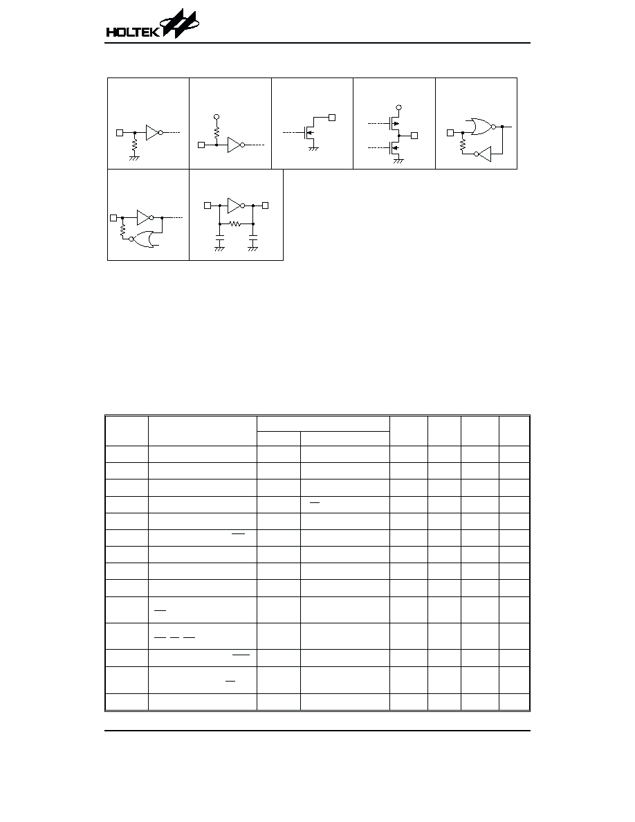
Approximate internal connection circuits
Absolute Maximum Ratings
Supply Voltage ............................................-0.3V to 5V
Storage Temperature ............................-50∞C to 125∞C
Input Voltage..............................V
SS
-0.3V to V
DD
+0.3V
Operating Temperature...........................-20∞C to 75∞C
Note: These are stress ratings only. Stresses exceeding the range specified under ≤Absolute Maximum Ratings≤ may
cause substantial damage to the device. Functional operation of this device at other conditions beyond those
listed in the specification is not implied and prolonged exposure to extreme conditions may affect device reliabil-
ity.
Electrical Characteristics
f
OSC
=32768Hz, Ta=25∞C
Symbol
Parameter
Test Conditions
Min.
Typ.
Max.
Unit
V
DD
Conditions
V
DD
Operating Voltage
æ
æ
1.2
1.5
1.7
V
V
IL
Input Low Voltage
1.2V~1.7V
æ
V
SS
æ
0.2V
DD
V
V
IH
Input High Voltage
1.2V~1.7V
æ
0.8V
DD
æ
V
DD
V
I
STB
Standby Current
1.5V
V
HK
=Floating (or V
DD
)
æ
0.1
1
mA
I
DD
Operating Current
1.5V
No load
æ
3
10
mA
I
OL
Output Sink Current of INT
1.5V
V
O
=0.3V
500
1000
æ
mA
t
A
Data Setup Time
1.5V
æ
1
æ
æ
ms
t
B
Data Hold on Time
1.5V
æ
2
æ
æ
ms
t
C
Inter Digit Time
1.5V
æ
5
æ
æ
ms
t
DB
Debounce Time
(HK, S1, S2, TIMER)
1.5V
æ
æ
31.25
æ
ms
R
HI1
Pull-high Resistance
(HK, DI, SK)
1.5V
V
IN
=0V
æ
1
æ
MW
R
HI2
Pull-high Resistance (RES)
1.5V
V
IN
=0V
100
200
400
kW
R
LO
Pull-low Resistance
(TIMER, S1, S2, 12/24)
1.5V
V
IN
=1.5V
æ
5
æ
MW
f
OSC
System Frequency
1.5V
Crystal=32768Hz
æ
32768
æ
Hz
HT1613C
Rev. 1.10
4
August 17, 2001
C M O S L A T C H I N
P u l l - h i g h
C M O S L A T C H I N
P u l l - l o w
P W R O N
1 5 k W
N M O S O U T
C M O S I N
P u l l - l o w
C M O S I N
P u l l - h i g h
O S C I L L A T O R
C M O S O U T
X 1
1 2 p F
1 5 p F
1 0 M W
V
D D
P W R O N
1 5 k W
X 2
V
D D

Functional Description
Operational flow chart
HT1613C
Rev. 1.10
5
August 17, 2001
EPN="0" ?
Power-on
RT="1" ?
Blank
Real time clock
HK="0" ?
Blinking"
"
ACT="0" ?
Dialing?
Display no.
TIMER input?
Dialing?
Display no.
Over 10 secs?
TIMER input?
Reset timer &
start counting
Keep counting
Dialing?
TIMER input?
Hold timer
Dialing?
TIMER input?
TIMER input?
Display last timer value
Over 9 secs?
TIMER input?
Display no.
TIMER input?
Over 10 secs?
Display last
timer value
Over 9 secs?
N
Y
N
N
N
N
N
N
Y
N
N
N
Y
Y
Y
Y
Y
N
Y
Y
N
Y
Y
N
Y
N
N
Y
Y
N
N
Y
N
Y
N
Y
N
Y
N
Y
N
Y
N
Y
Y
Display no.
TIMER input?
Over 10 secs?
Y
Y
N
Y
Y
N
N
N
N
Y
Y
Y
Y
N
HK="0" ?
HK="0" ?
HK="0" ?
HK="0" ?
HK="0" ?
HK="0" ?
HK="0" ?
HK="0" ?
EPN="0" ?
N