 | ÐлекÑÑоннÑй компоненÑ: HT23C040 | СкаÑаÑÑ:  PDF PDF  ZIP ZIP |
Äîêóìåíòàöèÿ è îïèñàíèÿ www.docs.chipfind.ru
HT23C040
CMOS 512K´8-Bit Mask ROM
1
January 20, 2000
Features
·
Operating voltage: 2.7V~5.5V
·
Low power consumption
Operation: 25mA max. (V
CC
=5V)
10mA max. (V
CC
=3V)
Standby: 30mA max. (V
CC
=5V)
10mA max. (V
CC
=3V)
·
Access time: 120ns max. (V
CC
=5V)
250ns max. (V
CC
=3V)
·
524288´8-bit of mask ROM
·
Mask option: chip enable CE/CE/OE1/OE1,
and output enable OE/OE/NC
·
TTL compatible inputs and outputs
·
Tristate outputs
·
Fully static operation
·
Package type: 32-pin DIP/SOP
General Description
The HT23C040 is a read-only memory with
high performance CMOS storage device whose
4096K of memory is arranged into 524288 word
by 8 bits.
For application flexibility, the chip enable and
output enable control pins can be selected as ac-
tive high or active low. This flexibility not only
allows easy interface with most microproces-
sors, but also eliminates bus contention in mul-
tiple bus microprocessor systems. An
additional feature of the HT23C040 is its abil-
ity to enter the standby mode whenever the
chip enable (CE/CE) is inactive, thus reducing
current consumption to below 30mA. The combi-
nation of these functions makes the chip suit-
able for high density low power memory
applications.
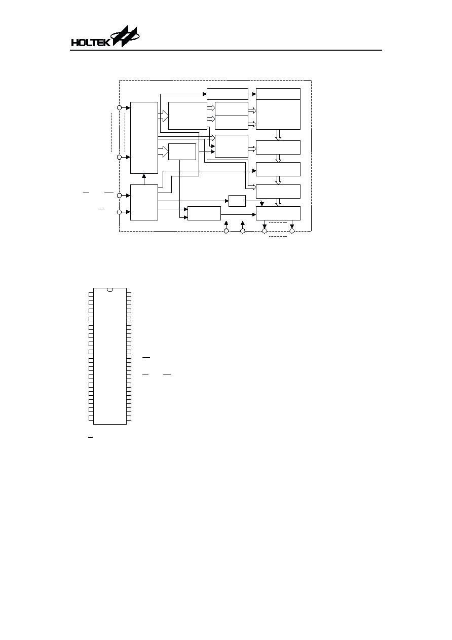
Block Diagram
Pin Assignment
HT23C040
2
January 20, 2000
A 0
A 1 8
R O M C e l l
A r r a y
( 5 1 2 K ´ 8 - B i t s )
C T R L
Z - D e c
Z - s e l e c t o r
S e n s e A m p l i f i e r s
O u t p u t B u f f e r s
V S S
V C C
D 7
C E / C E / O E 1 / O E 1
A d d r e s s
B u f f e r s
D 0
O E / O E / N C
P u l l - h i g h N M O S
M u x
P r e - c h a r g e C K T
X Y
P r e - d e c o d e r
A T D
L a t c h
Y - D e c
X - D e c
M u x
V C C
A 1 8
A 1 7
A 1 4
A 1 3
A 8
A 9
A 1 1
O E / O E / N C
A 1 0
C E / C E / O E 1 / O E 1
D 7
D 6
D 5
D 4
D 3
N C
A 1 6
A 1 5
A 1 2
A 7
A 6
A 5
A 4
A 3
A 2
A 1
A 0
D 0
D 1
D 2
V S S
1
2
3
4
5
6
7
8
9
1 0
1 1
1 2
1 3
1 4
1 5
1 6
3 2
3 1
3 0
2 9
2 8
2 7
2 6
2 5
2 4
2 3
2 2
2 1
2 0
1 9
1 8
1 7
H T 2 3 C 0 4 0
3 2 D I P / S O P
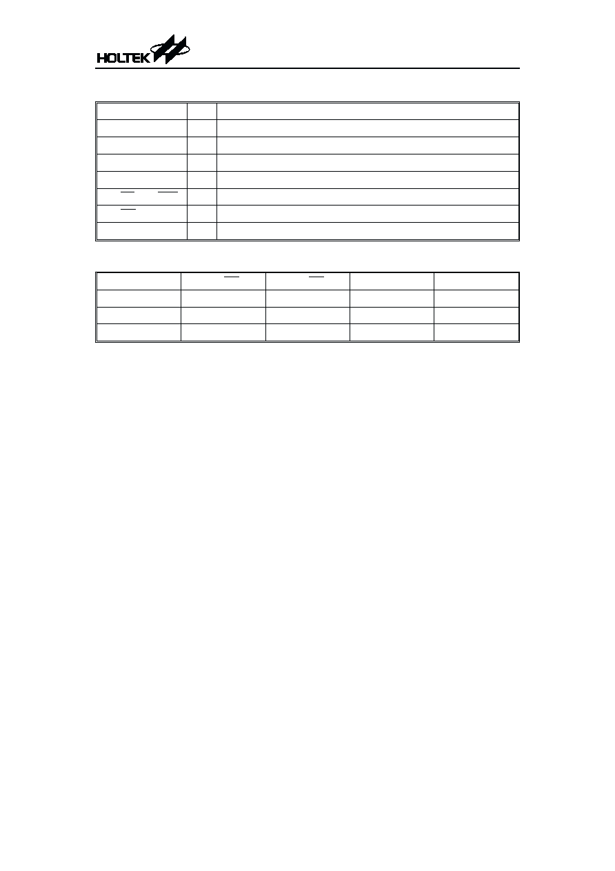
Pin Description
Pin Name
I/O
Description
NC
¾
No connection
A0~A18
I
Address inputs
D0~D7
O
Data outputs
VSS
¾
Negative power supply
CE/CE/OE1/OE1
I
Chip enable/Output enable input
OE/OE/NC
I
Output enable input
VCC
¾
Positive power supply
Operation Truth Table
Mode
CE/CE
OE/OE
A0~A18
D0~D7
Read
H/L
H/L
Valid
Data Out
Deselect
H/L
L/H
X
High Z
Standby
L/H
X
X
High Z
Note: H=V
IH
, L=V
IL
, X=V
IH
or V
IL
Absolute Maximum Ratings
Supply Voltage.................................-0.3V to 6V
Storage Temperature.................-50°C to 125°C
Input Voltage .......................-0.3V to V
CC
+0.3V
Operating Temperature ..............-40°C to 85°C
Note: These are stress ratings only. Stresses exceeding the range specified under ²Absolute Maxi-
mum Ratings² may cause substantial damage to the device. Functional operation of this device
at other conditions beyond those listed in the specification is not implied and prolonged expo-
sure to extreme conditions may affect device reliability.
HT23C040
3
January 20, 2000
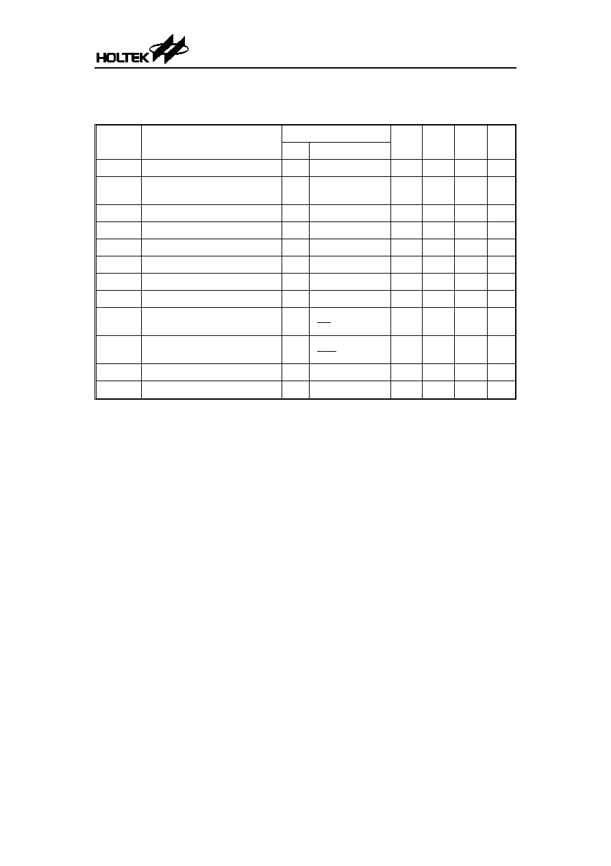
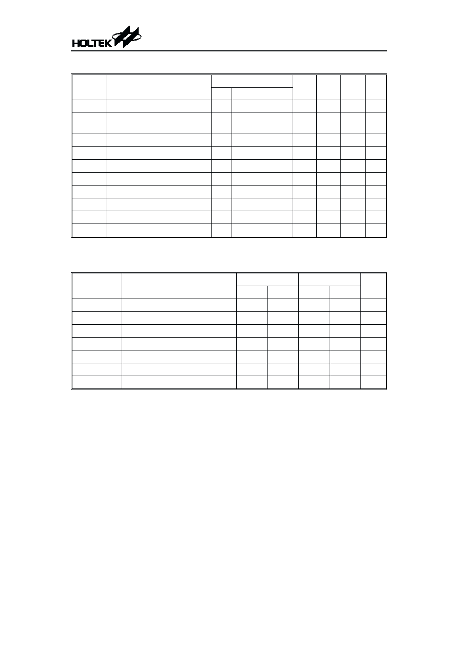
D.C. Characteristics
Supply voltage: 4.5V~5.5V
T
a
=-40°C to 85°C
Symbol
Parameter
Test Conditions
Min. Typ. Max. Unit
V
CC
Conditions
V
CC
Operating Voltage
¾
¾
4.5
¾
5.5
V
I
CC1
Operating Current
5V
O/P Unload,
f=5MHz
¾
¾
25
mA
V
IL1
Input Low Voltage
5V
¾
V
SS
¾
0.8
V
V
IH1
Input High Voltage
5V
¾
2.2
¾
V
CC
V
V
OL1
Output Low Voltage
5V
I
OL
=3.2mA
¾
¾
0.4
V
V
OH1
Output High Voltage
5V
I
OH
=-1mA
2.4
¾
V
CC
V
I
LI
Input Leakage Current
5V
V
IN
=0 to V
CC
¾
¾
10
mA
I
LO
Output Leakage Current
5V
V
OUT
=0 to V
CC
¾
¾
10
mA
I
STB1
Standby Current
5V
CE=V
IL
CE=V
IH
¾
¾
1.5
mA
I
STB2
Standby Current
5V
CE£0.2V
CE³V
CC
-0.2V
¾
¾
30
mA
C
IN
Input Capacitance (See note)
¾
f=1MHz
¾
¾
10
pF
C
OUT
Output Capacitance (See note)
¾
f=1MHz
¾
¾
10
pF
HT23C040
4
January 20, 2000
Supply voltage: 2.7V~3.3V
T
a
=-40°C to 85°C
Symbol
Parameter
Test Conditions
Min. Typ. Max. Unit
V
CC
Conditions
V
CC
Operating Voltage
¾
¾
2.7
¾
3.3
V
I
CC2
Operating Current
3V
O/P Unload,
f=5MHz
¾
¾
10
mA
V
IL2
Input Low Voltage
3V
¾
V
SS
¾
0.4
V
V
IH2
Input High Voltage
3V
¾
1.5
¾
V
CC
V
V
OL2
Output Low Voltage
3V
I
OL
=2mA
¾
¾
0.4
V
V
OH2
Output High Voltage
3V
I
OH
=-0.6mA
1.5
¾
V
CC
V
I
LI
Input Leakage Current
3V
V
IN
=0 to V
CC
¾
¾
10
mA
I
LO
Output Leakage Current
3V
V
OUT
=0 to V
CC
¾
¾
10
mA
C
IN
Input Capacitance (See Note)
¾
f=1MHz
¾
¾
10
pF
C
OUT
Output Capacitance (See Note)
¾
f=1MHz
¾
¾
10
pF
Note: These parameters are periodically sampled but not 100% tested.
A.C. Characteristics
T
a
=-40°C to 85°C
Symbol
Parameter
3V±10%
5V±10%
Unit
Min.
Max.
Min.
Max.
t
CYC
Cycle Time
200
¾
120
¾
ns
t
AA
Address Access Time
¾
250
¾
120
ns
t
ACE
Chip Enable Access Time
¾
250
¾
120
ns
t
AOE
Output Enable Access Time
¾
150
¾
80
ns
t
OH
Output Hold Time
¾
¾
10
¾
ns
t
OD
Output Disable Time (See Note)
¾
¾
¾
70
ns
t
OE
Output Enable Time (See Note)
¾
¾
10
¾
ns
Note: These parameters are periodically sampled but not 100% tested.
HT23C040
5
January 20, 2000
Document Outline
- þÿ
- þÿ
- þÿ
- þÿ
- þÿ
- þÿ
- þÿ
- þÿ
- þÿ
- þÿ
- þÿ
- þÿ
- þÿ