 | ÐлекÑÑоннÑй компоненÑ: HT48C062 | СкаÑаÑÑ:  PDF PDF  ZIP ZIP |
HT48R062/HT48C062 --
Cost-Effective I/O Type 8-Bit MCU
HT48R062/HT48C062
Cost-Effective I/O Type 8-Bit MCU
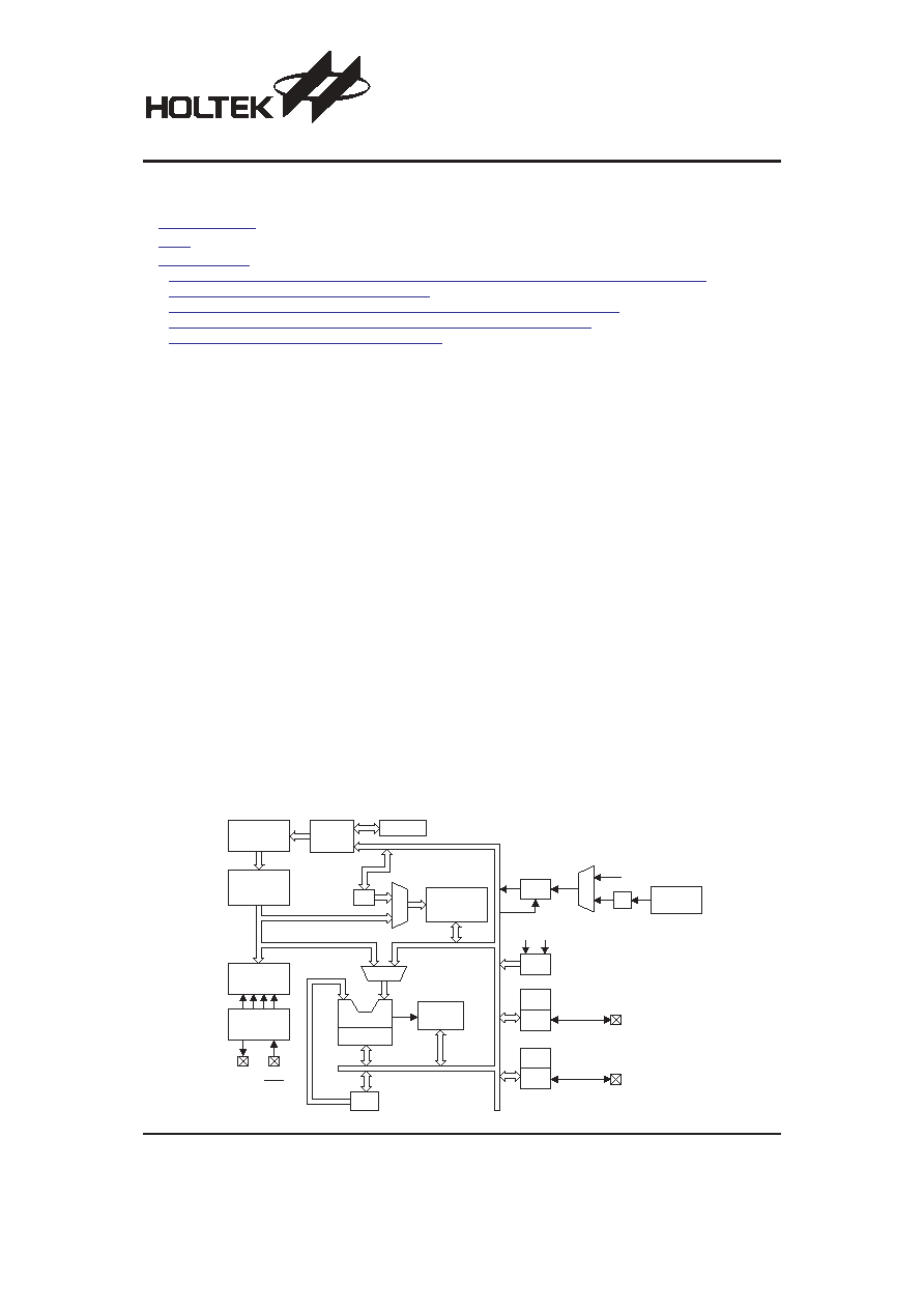
Block Diagram
Rev. 1.00
1
July 13, 2006
Features
·
Operating voltage:
f
SYS
=4MHz: 2.2V~5.5V
f
SYS
=8MHz: 3.3V~5.5V
·
11 bidirectional I/O lines
·
On-chip crystal and RC oscillator
·
Watchdog Timer
·
1K
´14 program memory
·
32
´8 data RAM
·
HALT function and wake-up feature reduce power
consumption
·
63 powerful instructions
·
Up to 0.5
ms instruction cycle with 8MHz system clock
·
All instructions in 1 or 2 machine cycles
·
14-bit table read instructions
·
One-level subroutine nesting
·
Bit manipulation instructions
·
Low voltage reset function
·
16-pin DIP/SOP/SSOP package
General Description
The HT48R062/HT48C062 are 8-bit high performance,
RISC architecture microcontroller devices specifically
designed for cost-effective multiple I/O control product
applications. The mask version HT48C062 is fully pin
and functionally compatible with the OTP version
HT48R062 devices.
The advantages of low power consumption, I/O flexibil-
ity, oscillator options, HALT and wake-up functions,
watchdog timer, as well as low cost, enhance the versa-
tility of these devices to suit a wide range of application
possibilities such as industrial control, consumer prod-
ucts, subsystem controllers, etc.
The HT48C062 is under development and will be avail-
able soon.
Technical Document
·
Tools Information
·
FAQs
·
Application Note
-
HA0003E Communicating between the HT48 & HT46 Series MCUs and the HT93LC46 EEPROM
-
HA0013E HT48 & HT46 LCM Interface Design
-
HA0016E Writing and Reading to the HT24 EEPROM with the HT48 MCU Series
-
HA0018E Controlling the HT1621 LCD Controller with the HT48 MCU Series
-
HA0049E Read and Write Control of the HT1380
P r o g r a m
C o u n t e r
P r o g r a m
I n s t r u c t i o n
R e g i s t e r
I n s t r u c t i o n
D e c o d e r
T i m i n g
G e n e r a t o r
O S C 2
O S C 1
R E S
V D D
V S S
M P
M
U
X
M U X
D a t a
M e m o r y
A L U
S h i f t e r
S T A T U S
A C C
S t a c k
W D T
S y s t e m C l o c k / 4
W D T O S C
( 2 4 k H z )
¸ 2
P B C
P B
P o r t B
P B 0 ~ P B 2
P A C
P A
P A 0 ~ P A 7
P o r t A
M
U
X
L V R
H A L T E N / D I S
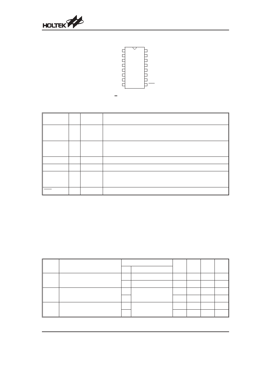
Pin Assignment
Pin Description
Pin Name
I/O
Code
Option
Description
PA0~PA7
I/O
Pull-high
Wake-up
Bidirectional 8-bit input/output port. Each bit can be configured as wake-up in-
put by options. Software instructions determine the CMOS output or Schmitt
trigger input with a pull-high resistor (determined by pull-high options).
PB0~PB2
I/O
Pull-high
Bidirectional 3-bit input/output port. Software instructions determine the
CMOS output or Schmitt trigger input with a pull-high resistor (determined by
pull-high options).
VDD
¾
¾
Positive power supply
VSS
¾
¾
Negative power supply, ground
OSC2
OSC1
O
I
Crystal
or RC
OSC1, OSC2 are connected to an RC network or a crystal (determined by
code option) for the internal system clock. In the case of RC operation, OSC2
is the output terminal for 1/4 system clock (NMOS open drain output).
RES
I
¾
Schmitt trigger reset input. Active low.
Absolute Maximum Ratings
Supply Voltage ...........................V
SS
-0.3V to V
SS
+6.0V
Storage Temperature ............................
-50°C to 125°C
Input Voltage..............................V
SS
-0.3V to V
DD
+0.3V
Operating Temperature...........................
-40°C to 85°C
Note: These are stress ratings only. Stresses exceeding the range specified under
²Absolute Maximum Ratings² may
cause substantial damage to the device. Functional operation of this device at other conditions beyond those
listed in the specification is not implied and prolonged exposure to extreme conditions may affect device reliabil-
ity.
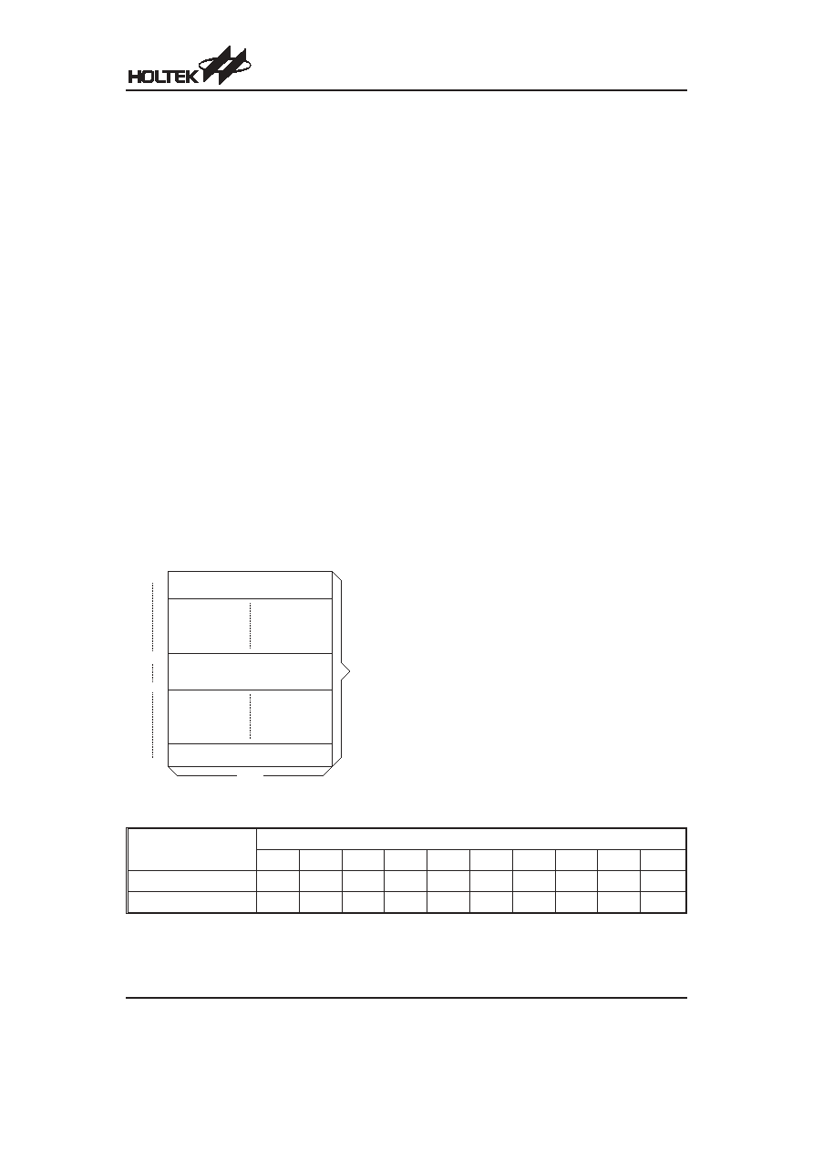
D.C. Characteristics
Ta=25
°C
Symbol
Parameter
Test Conditions
Min.
Typ.
Max.
Unit
V
DD
Conditions
V
DD
Operating Voltage
¾ f
SYS
=4MHz
2.2
¾
5.5
V
¾ f
SYS
=8MHz
3.3
¾
5.5
V
I
DD1
Operating Current (Crystal OSC)
3V
No load, f
SYS
=4MHz
¾
0.6
1.5
mA
5V
¾
2
4
mA
I
DD2
Operating Current (RC OSC)
3V
No load, f
SYS
=4MHz
¾
0.8
1.5
mA
5V
¾
2.5
4
mA
HT48R062/HT48C062
Rev. 1.00
2
July 13, 2006
H T 4 8 R 0 6 2 / H T 4 8 C 0 6 2
1 6 D I P - A / S O P - A / S S O P - A
1 6
1 5
1 4
1 3
1 2
1 1
1 0
9
1
2
3
4
5
6
7
8
P A 4
P A 5
P A 6
P A 7
O S C 2
O S C 1
V D D
R E S
P A 3
P A 2
P A 1
P A 0
P B 0
V S S
P B 1
P B 2
Symbol
Parameter
Test Conditions
Min.
Typ.
Max.
Unit
V
DD
Conditions
I
DD3
Operating Current
(Crystal OSC, RC OSC)
5V
No load, f
SYS
=8MHz
¾
4
8
mA
I
STB1
Standby Current (WDT Enabled)
3V
No load, system HALT
¾
¾
5
mA
5V
¾
¾
10
mA
I
STB2
Standby Current (WDT Disabled)
3V
No load, system HALT
¾
¾
1
mA
5V
¾
¾
2
mA
V
IL1
Input Low Voltage for I/O Port
¾
¾
0
¾
0.3V
DD
V
V
IH1
Input High Voltage for I/O Port
¾
¾
0.7V
DD
¾
V
DD
V
V
IL2
Input Low Voltage (RES)
¾
¾
0
¾
0.4V
DD
V
V
IH2
Input High Voltage (RES)
¾
¾
0.9V
DD
¾
V
DD
V
V
LVR
Low Voltage Reset
¾ LVRenabled
2.7
3
3.3
V
I
OL
I/O Port Sink Current
3V
V
OL
=0.1V
DD
4
8
¾
mA
5V
10
20
¾
mA
I
OH
I/O Port Source Current
3V
V
OH
=0.9V
DD
-2
-4
¾
mA
5V
-5
-10
¾
mA
R
PH
Pull-high Resistance
3V
¾
20
60
100
k
W
5V
10
30
50
k
W
A.C. Characteristics
Ta=25
°C
Symbol
Parameter
Test Conditions
Min.
Typ.
Max.
Unit
V
DD
Conditions
f
SYS1
System Clock (Crystal OSC)
¾ 2.2V~5.5V
400
¾
4000
kHz
¾ 3.3V~5.5V
400
¾
8000
kHz
f
SYS2
System Clock (RC OSC)
¾ 2.2V~5.5V
400
¾
4000
kHz
¾ 3.3V~5.5V
400
¾
8000
kHz
t
WDTOSC
Watchdog Oscillator Period
3V
¾
22
45
90
ms
5V
16
32
64
ms
t
RES
External Reset Low Pulse Width
¾
¾
1
¾
¾
ms
t
SST
System Start-up Timer Period
¾
Power-up or wake-up
from HALT
¾
1024
¾
t
SYS
t
LVR
Low Voltage Width to Reset
¾
¾
0.25
1
2
ms
Note: t
SYS
=1/f
SYS
HT48R062/HT48C062
Rev. 1.00
3
July 13, 2006
HT48R062/HT48C062
Rev. 1.00
4
July 13, 2006
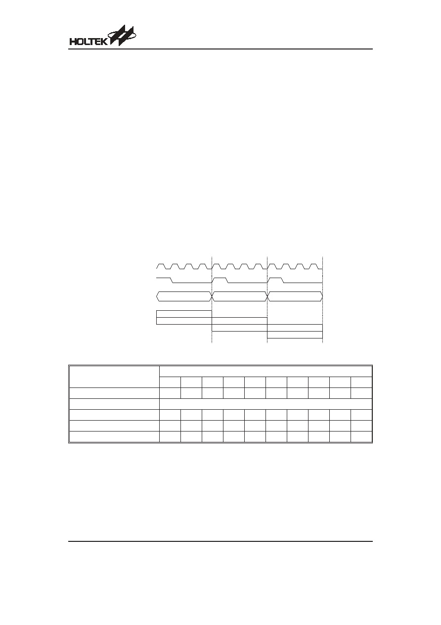
Functional Description
Execution Flow
The HT48R062/HT48C062 system clock can be derived
from a crystal/ceramic resonator oscillator or an RC. It is
internally divided into four non-overlapping clocks. One
instruction cycle consists of four system clock cycles.
Instruction fetching and execution are pipelined in such
a way that a fetch takes an instruction cycle while de-
coding and execution takes the next instruction cycle.
However, the pipelining scheme causes each instruc-
tion to effectively execute in a cycle. If an instruction
changes the program counter, two cycles are required to
complete the instruction.
Program Counter
- PC
The 10-bit program counter (PC) controls the sequence
in which the instructions stored in program ROM are ex-
ecuted and its contents specify a maximum of 1024 ad-
dresses.
After accessing a program memory word to fetch an in-
struction code, the contents of the program counter are
incremented by one. The program counter then points to
the memory word containing the next instruction code.
When executing a jump instruction, conditional skip ex-
ecution, loading PCL register, subroutine call, initial re-
set or return from subroutine, the PC manipulates the
program transfer by loading the address corresponding
to each instruction.
The conditional skip is activated by instruction. Once the
condition is met, the next instruction, fetched during the
current instruction execution, is discarded and a dummy
cycle replaces it to get the proper instruction. Otherwise
proceed with the next instruction.
The lower byte of the program counter (PCL) is a read-
able and writeable register (06H). Moving data into the
PCL performs a short jump. The destination will be
within 256 locations.
When a control transfer takes place, an additional
dummy cycle is required.
T 1
T 2
T 3
T 4
T 1
T 2
T 3
T 4
T 1
T 2
T 3
T 4
F e t c h I N S T ( P C )
E x e c u t e I N S T ( P C - 1 )
F e t c h I N S T ( P C + 1 )
E x e c u t e I N S T ( P C )
F e t c h I N S T ( P C + 2 )
E x e c u t e I N S T ( P C + 1 )
P C
P C + 1
P C + 2
S y s t e m C l o c k
I n s t r u c t i o n C y c l e
P C
Execution Flow
Mode
Program Counter
*9
*8
*7
*6
*5
*4
*3
*2
*1
*0
Initial Reset
0
0
0
0
0
0
0
0
0
0
Skip
Program Counter+2
Loading PCL
*9
*8
@7
@6
@5
@4
@3
@2
@1
@0
Jump, Call Branch
#9
#8
#7
#6
#5
#4
#3
#2
#1
#0
Return from Subroutine
S9
S8
S7
S6
S5
S4
S3
S2
S1
S0
Program Counter
Note:
*9~*0: Program counter bits
S9~S0: Stack register bits
#9~#0: Instruction code bits
@7~@0: PCL bits
HT48R062/HT48C062
Rev. 1.00
5
July 13, 2006
Program Memory
- ROM
The program memory is used to store the program in-
structions which are to be executed. It also contains
data and table and is organized into 1024
´14 bits, ad-
dressed by the program counter and table pointer.
Certain locations in the program memory are reserved
for special usage:
·
Location 000H
This area is reserved for the initialization program. Af-
ter chip reset, the program always begins execution at
location 000H.
·
Table location
Any location in the EPROM space can be used as
look-up tables. The instructions
²TABRDC [m]² (the
current page, one page=256 words) and
²TABRDL
[m]
² (the last page) transfer the contents of the
lower-order byte to the specified data memory, and
the higher-order byte to TBLH (08H). Only the desti-
nation of the lower-order byte in the table is
well-defined, the other bits of the table word are trans-
ferred to the lower portion of TBLH, the remaining 2
bits are read as
²0². The Table Higher-order byte reg-
ister (TBLH) is read only. The table pointer (TBLP) is a
read/write register (07H), where P indicates the table
location. Before accessing the table, the location must
be placed in TBLP. The TBLH is read only and cannot
be restored. All table related instructions need 2 cy-
cles to complete the operation. These areas may
function as normal program memory depending upon
the requirements.
Stack Register
- STACK
This is a special part of the memory used to save the
contents of the Program Counter only. The stack is orga-
nized into one level and is neither part of the data nor
part of the program space, and is neither readable nor
writeable. The activated level is indexed by the stack
pointer (SP) and is neither readable nor writeable. At a
subroutine call the contents of the program counter are
pushed onto the stack. At the end of a subroutine sig-
naled by a return instruction (RET), the program counter
is restored to its previous value from the stack. After a
chip reset, the SP will point to the top of the stack.
If the stack is full and a
²CALL² is subsequently exe-
cuted, stack overflow occurs and the first entry will be
lost (only the most recent return address is stored).
Data Memory
- RAM
The data memory is designed with 44
´8 bits. The data
memory is divided into two functional groups: special
function registers and general purpose data memory
(32
´8). Most of them are read/write, but some are read
only.
The special function registers include the Indirect Ad-
dressing Register (00H), the Memory Pointer register
(MP;01H), the Accumulator (ACC;05H) the Program
Counter Lower-order byte register (PCL;06H), the Table
Pointer (TBLP;07H), the table higher-order byte register
(TBLH;08H), the Watchdog Timer option setting register
(WDTS;09H), the STATUS register (STATUS;0AH), the
I/O registers (PA;12H, PB;14H) and I/O control registers
(PAC;13H, PBC;15H). The remaining space before the
20H is reserved for future expanded usage and reading
these locations will return the result 00H. The general
purpose data memory, addressed from 20H to 3FH, is
used for data and control information under instruction
command.
All data memory areas can handle arithmetic, logic, in-
crement, decrement and rotate operations directly. Ex-
cept for some dedicated bits, each bit in the data
memory can be set and reset by the
²SET [m].i² and
²CLR [m].i² instructions, respectively. They are also indi-
rectly accessible through memory pointer register
(MP;01H).
0 0 0 H
D e v i c e i n i t i a l i z a t i o n p r o g r a m
P r o g r a m
1 4 b i t s
L o o k - u p t a b l e ( 2 5 6 w o r d s )
n 0 0 H
L o o k - u p t a b l e ( 2 5 6 w o r d s )
3 F F H
N o t e : n r a n g e s f r o m 0 t o 3
n F F H
Program Memory
Instruction(s)
Table Location
*9
*8
*7
*6
*5
*4
*3
*2
*1
*0
TABRDC [m]
P9
P8
@7
@6
@5
@4
@3
@2
@1
@0
TABRDL [m]
1
1
@7
@6
@5
@4
@3
@2
@1
@0
Table Location
Note:
*9~*0: Table location bits
@7~@0: Table pointer bits
P9~P8: Current program counter bits
Document Outline
- þÿ
- þÿ
- þÿ
- þÿ
- þÿ
- þÿ
- þÿ
- þÿ
- þÿ
- þÿ
- þÿ
- þÿ
- þÿ
- þÿ
- þÿ