 | ÐлекÑÑоннÑй компоненÑ: HT9274 | СкаÑаÑÑ:  PDF PDF  ZIP ZIP |
Äîêóìåíòàöèÿ è îïèñàíèÿ www.docs.chipfind.ru
HT9274
Quad Micropower Op Amp
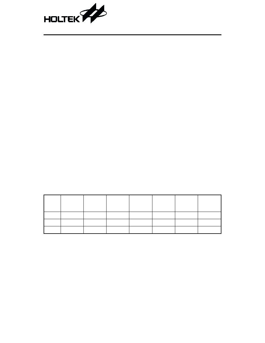
Comparison Table
ITEM Operating
Voltage
Operating
Current
Output
Source
Current
Output
Sink
Current
Input Bias
Current
GBW
Max. load
(To VDD
or VSS)
HT9274 1.6~5.5V
5mA
500mA
500mA
1pA
0.1MHz
>10kW
WT274
1.35~10V
9mA
16mA
2mA
1pA
0.1MHz
>500kW
LM324
3~32V
400mA
20mA
8mA
45nA
1MHz
>2kW
1
November 23, 1999
General Description
The HT9274 is a CMOS quad micro-power op-
erational amplifier featuring high input imped-
ance, extremely low power, high gain and high
stability.
It allows common mode input voltage range
which extends below the negative rail, output
swings to both rails with a reasonable sink and
souce capability of the output drive current.
This cost-effective device is suitable for high
gain, low frequency, low power applications, es-
pecially ideal for battery powered systems
where mA range of standby current is essential
for long battery life span. For example, in
multi-standard Caller ID systems, HT9274 is
ideal as a low power line signal monitor/detec-
tor, and in car alarm systems, the HT9274 is ex-
cellent for piezo vibratile detector signal
amplifier application.
Features
·
Quad micro power op amp
·
Wide range of supply voltage: 1.6V~5.5V
·
High input impedance
·
Single supply operation
·
Low current consumption: < 5mA per amp
·
Rail to rail output
·
Provides both sink and source output drive
capability
·
Common mode input extends below nega-
tive rail
·
Pin compatible with LM324/WT274 (14-pin
DIP)
·
14-pin DIP/SOP package
Applications
·
Battery powered system
·
Sensor amplifier
·
Low power gain blocks
·
Low power comparators
·
Signal detectors
·
Active filters
·
Caller ID systems
·
Communication systems
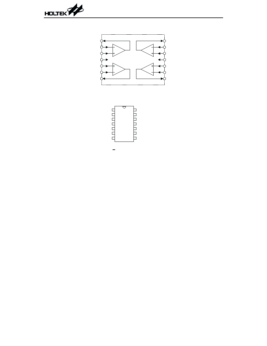
Block Diagram
Pin Assignment
HT9274
2
November 23, 1999
1 O U T
1 I N -
1 I N +
V D D
2 I N +
2 I N -
2 O U T
4 O U T
4 I N -
4 I N +
V S S
3 I N +
3 I N -
3 O U T
1 4
1 3
1 2
1 1
1 0
9
8
1
2
3
4
5
6
7
1 O U T
1 I N -
1 I N +
V D D
2 I N +
2 I N -
2 O U T
4 O U T
4 I N -
4 I N +
V S S
3 I N +
3 I N -
3 O U T
H T 9 2 7 4
1 4 D I P / S O P
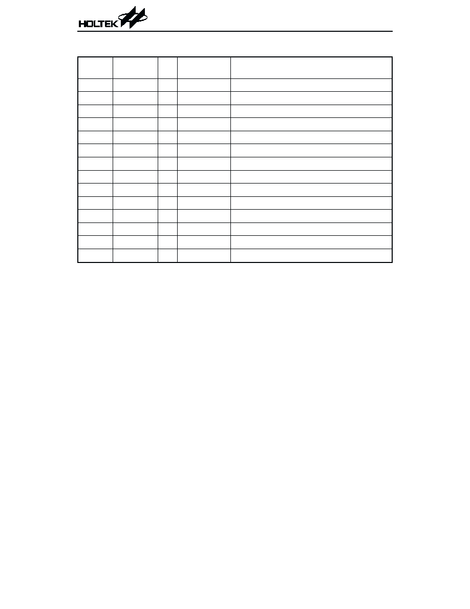
Pin Description
Pin No. Pin Name
I/O
Internal
Connection
Description
1
1OUT
O
CMOS OUT Output pin of the op amp 1
2
1IN-
I
PMOS IN
Inverting input pin of the op amp 1
3
1IN+
I
PMOS IN
Noninverting input pin of the op amp 1
4
VDD
¾
¾
Positive power supply
5
2IN+
I
PMOS IN
Noninverting input pin of the op amp 2
6
2IN-
I
PMOS IN
Inverting input pin of the op amp 2
7
2OUT
O
CMOS OUT Output pin of the op amp 2
8
3OUT
O
CMOS OUT Output pin of the op amp 3
9
3IN-
I
PMOS IN
Inverting input pin of the op amp 3
10
3IN+
I
PMOS IN
Noninverting input pin of the op amp 3
11
VSS
¾
¾
Negative power supply
12
4IN+
I
PMOS IN
Noninverting input pin of the op amp 4
13
4IN-
I
PMOS IN
Inverting input pin of the op amp 4
14
4OUT
O
CMOS OUT Output pin of the op amp 4
Absolute Maximum Ratings
Supply Voltage.................................-0.3V to 6V
Storage Temperature.................-50°C to 125°C
Input Voltage.................V
SS
-0.3V to V
DD
+0.3V
Operating Temperature ..............-20°C to 75°C
Note: These are stress ratings only. Stresses exceeding the range specified under "Absolute Maxi-
mum Ratings" may cause substantial damage to the device. Functional operation of this device
at other conditions beyond those listed in the specification is not implied and prolonged expo-
sure to extreme conditions may affect device reliability.
HT9274
3
November 23, 1999

Pin Description
Pin No. Pin Name
I/O
Internal
Connection
Description
1
1OUT
O
CMOS OUT Output pin of the op amp 1
2
1IN-
I
PMOS IN
Inverting input pin of the op amp 1
3
1IN+
I
PMOS IN
Noninverting input pin of the op amp 1
4
VDD
¾
¾
Positive power supply
5
2IN+
I
PMOS IN
Noninverting input pin of the op amp 2
6
2IN-
I
PMOS IN
Inverting input pin of the op amp 2
7
2OUT
O
CMOS OUT Output pin of the op amp 2
8
3OUT
O
CMOS OUT Output pin of the op amp 3
9
3IN-
I
PMOS IN
Inverting input pin of the op amp 3
10
3IN+
I
PMOS IN
Noninverting input pin of the op amp 3
11
VSS
¾
¾
Negative power supply
12
4IN+
I
PMOS IN
Noninverting input pin of the op amp 4
13
4IN-
I
PMOS IN
Inverting input pin of the op amp 4
14
4OUT
O
CMOS OUT Output pin of the op amp 4
HT9274
4
November 23, 1999
HT9274
5
November 23, 1999
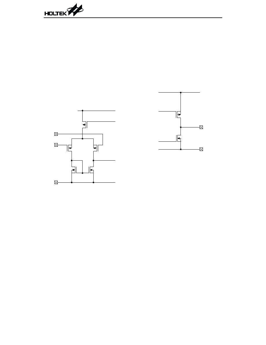
Functional Description
Input stage
The input stage of op amps are nominal PMOS
differential amplifiers (see the following dia-
gram), therefore the common mode input volt-
age can extend to V
SS
-0.6V. On the other hand
the common mode input voltage has to be main-
tained below (V
DD
-1)V to keep the input device
(M2 and M3) active. This implies that when us-
ing HT9274 as a voltage follower, the input as
well as output active range will be limited be-
tween V
SS
~ V
DD
-1V (approx.). Avoid applying
any voltage greater than V
DD
+0.6V or less than
V
SS
-0.6V to the input pins, otherwise the inter-
nal input protection devices may be damaged.
Since the input impedance of PMOS is inher-
ently very high, it can directly couple to high
impedance elements without loading effect. For
example, coupling to ceramic transducers, inte-
grating capacitor and resistor networks.
Actually the extremly high input impedance is
its major advantage over the bipolar counter-
part, in some application fields such as integra-
tors where the input current of op amp can
cause significant error, the HT9274 is a better
choice than the popular LM324.
Output stage
The HT9274 uses push-pull CMOS configura-
tion as the output stage of op amps to minimize
low power consumption and to provide ade-
quate output driving current.
Note that the output is an unbuffered struc-
ture, therefore the open loop gain will be af-
fected by the load resistor since the voltage gain
of this stage can be expressed as (gm5+
gm6)´R
L
.
Because of the consideration for minimized
power consumption, the max. output current is
limited to about 400mA for both source and sink
drive. This is believed to be enough for most low
power systems, however it is recommended to
use the load resistor of >10kW for normal appli-
cations. In case of heavy load driving, an exter-
nal buffer stage using bipolar transistors is
recommended.
The HT9274 is internally compensated for AC
stability and capable to withstand up to a
100pF capacitive load.
V
D D
V
B I A S
M 1
M 2
M 3
M 4
M 5
V
S S
V
S S
P M O S
P M O S
N o n i n v e r t i n g I n
I n v e r t i n g I n
T o O u t p u t S t a g e
M 5
M 6
V
D D
V
S S
O U T
V
B I A S
F r o m
D i f f e r e n t i a l
A m p
Document Outline
- þÿ
- þÿ
- þÿ
- þÿ
- þÿ
- þÿ
- þÿ
- þÿ
- þÿ
- þÿ
- þÿ