
HI-8010/HI-8110 Series
The HI-8010 & HI-8110 high voltage display drivers
are constructed of MOS P Channel and N Channel
enhancement mode devices in a single monolithic
structure. They are designed to drive high voltage
liquid crystal displays by converting low level input
signals (TTL on the HI-8010 and CMOS on the
HI-8110) to high voltage drive signals.
Both devices can drive up to 38 segments and
require minimal display-to-data source interfacing.
Serial data is loaded and held in internal latches until
new display data is received.
The HI-8010 & HI-8110 are available in a variety of
ceramic and plastic packaging including DIP; leaded
and leadless chip carriers; and J-lead and gull-wing
quad flat packs.
!
!
!
Dichroic Liquid Crystal Displays
Standard Liquid Crystal Displays
Vacuum Fluorescent Displays
!
!
!
!
!
!
!
!
!
5 volt input translated to 30 volts or less
Pin-out adaptable to drive 30, 32 or 38
LCD segments
RC oscillator or high voltage (BP) clock input
TTL compatible inputs (HI-8010 only)
CMOS compatible inputs (HI-8110 only)
Low power consumption
Industrial (-40∞C to +85∞C) & Military (-55∞C
to +125∞C) temperature ranges
Pin for pin compatible with the Micrel
MIC8010/8011 series and the AMI S4520
series drivers
Cascadable
Military level processing available
!
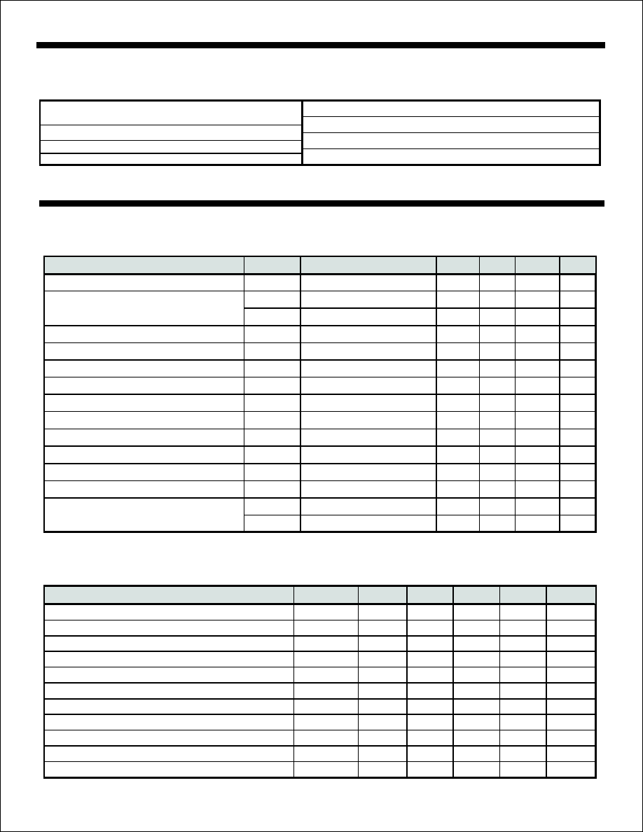
PIN CONFIGURATION
(Top View)
FUNCTIONAL BLOCK DIAGRAM
Þ
BP
O s c i l l a t o r
D i v i d e r
V o l t a g e
T r a n s l a t o r
H i g h V o l t a g e
B u f f e r
3 8 S t a g e
S h i f t R e g i s t e r
3 8 B i t L a t c h
V o l t a g e
T r a n s l a t o r s
H i g h V o l t a g e
D r i v e r s
SEGMENTS
DATA IN
CLK
LE
Þ
Þ
Þ
DOUT 38
DOUT 32
DOUT 30
GENERAL DESCRIPTION
DIN
Þ
CL
Þ
CS
Þ
LD
Þ
LCDÿ
Þ
LCDÿ OPT
Þ
(See page 3-6 for additional package pin configurations)
FEATURES
January 2001
39
38
37
36
35
34
33
32
31
30
29
28
S26
S25
S24
S23
S22
S21
S20
DOUT 38
N/C
N/C
N/C
BP
S19
2
3
4
5
6
7
8
9
10
11
12
LD
DIN
LCDÿ
LCDÿOPT
V
S37
S38
S1
S2
S3
S4
S5
S6
DD
HI-8010PQI
HI-8110PQI
HI-8010PQT
&
HI-8110PQT
52 - PIN
PLASTIC
P
QF
HOLT INTEGRATED CIRCUITS
3-3
(DS8010, Rev. C)
01/01

FUNCTIONAL DESCRIPTION
Whenever a Logic "0" is applied to the Chip Select (
)
input, one bit of data is clocked into the shift register from the
serial data input (DIN) with each negative transition of the
Clock (
) input.
is internally tied to VSS on some
versions. A Logic "1" present at the Load (LD) input will
cause a parallel transfer of data from the shift register to the
data latch. If the Load (LD) input is held high while data is
clocked into the shift register, the latch will be transparent.
To display segments, a Logic "1" is stored in the appropriate
shift register bit position, and the segment output is out-of-
phase with the backplane.
The backplane output functions in 1 of 2 modes; externally
driven or self-oscillating. When the LCDÿ input is externally
driven with the LCDÿOPT input open circuit (Figure 2), the
backplane output will be in-phase with LCDÿ. Utilizing the
self-oscillating mode, inputs LCDÿ and LCDÿOPT are tied
together and connected to an RC circuit (Figure 3).
A 150K
resistor with a 470pF capacitor generates an
approximate backplane frequency of 100Hz. The
LCDÿ/LCDÿOPT oscillator frequency is divided by 256 to
determine the backplane output frequency.
The resistor
value (R) must be at least 30K
for proper self-oscillator
operation.
For displays having a number of segments greater than 38,
two or more of the display drivers may be cascaded together
by connecting the serial data output (DOUT) from the first
driver, to the serial data input (DIN) of the following driver,
etc. (See Figures 2 & 3). Data out (DOUT) will change state
CS
CL
CS
W
All four logic inputs are TTL compatible on the HI-8010 and
CMOS compatible on the HI-8110.
W
HI-8010/HI-8110 Series
TIMING DIAGRAM
t
CSH
t
CSS
t
DS
t
DH
t
CL
t
CDO
t
LS
t
LW
t
CSL
t
LCS
CL
INPUT
DIN
INPUT
CS
INPUT
LD
INPUT
DOUT
OUTPUT
VALID
VALID
INTERNAL OSCILLATOR CIRCUIT
TO BACKPLANE
TRANSLATOR
AND DRIVER
˜ 256
LCDÿ
OPT
LCDÿ
Figure 1
Q
on the rising edge of the Clock (
). Clock (
), Load (LD)
and Chip Select (
) should be tied in common with each
other, respectively, between all cascaded display drivers.
CL
CL
CS
HOLT INTEGRATED CIRCUITS
3-4
HI-8010/HI-8110 Series
DC ELECTRICAL CHARACTERISTICS
VDD = 5V, VEE = -25V, VSS = 0V, TA = Operating Temperature Range (unless otherwise specified).
PARAMETER
SYMBOL
CONDITION
MIN
TYP
MAX
UNITS
Operating Voltage
VDD
3.0
7.0
V
Supply Current
IDD
Static, No Load
200
µA
IEE
Static, No Load f
=100Hz
150
µA
Input Low Voltage, HI-8010 (except LCDÿ)
VIL
0
0.8
V
Input High Voltage, HI-8010 (except LCDÿ)
VIH
2
VDD
V
Input Low Voltage, HI-8110 (except LCD )
VIL
0
0.3 VDD
V
Input High Voltage, HI-8110 (except LCD
Input Low Voltage (LCDÿ)
VILX
VEE
3
V
Input High Voltage (LCDÿ)
VIHX
3.5
VDD
V
Input Current
IIN
VIN = 0 to 5V
1
µA
Input Capacitance (not tested)
CI
5
pF
Segment Output Impedance
RSEG
IL = 10µA
10,000
Backplane Output Impedance
RBP
IL = 10µA
450
Data Out Current:
IDOH
Source Current, VOH = 4.5V
-0.6
mA
IDOL
Sink Current, VOL = 0.5V
0.6
mA
BP
TTL
TTL
CMOS
W
W
ÿ
ÿ)
VIH
0.7 VDD
VDD
V
CMOS
PARAMETER
SYMBOL
VDD
MIN
TYP
MAX
UNITS
CL
Clock Period
t
5V
1200
ns
Clock Pulse Width
t
5V
520
ns
Data In - Setup
t
5V
50
ns
Data In - Hold
t
5V
400
ns
Chip Select - Setup to Clock
t
5V
200
ns
Chip Select - Hold to Clock
t
5V
450
ns
Load - Setup to Clock
t
5V
500
ns
Chip Select - Setup to Load
t
5V
300
ns
Load Pulse Width
t
5V
500
ns
Chip Select - Hold to Load
t
5V
300
ns
CW
DS
DH
CSS
CSH
LS
CSL
LW
LCS
Data Out Valid, from Clock
t
5V
800
ns
CDO
AC ELECTRICAL CHARACTERISTICS
VDD = 5V, VEE = -25V, VSS = 0V, TA = Operating Temperature Range (unless otherwise specified).
ABSOLUTE MAXIMUM RATINGS
NOTE: Stresses above those listed under "Absolute Maximum Ratings" may cause permanent damage to the device. These are stress ratings only.
Functional operation of the device at these or any other conditions above those indicated in the operational sections of the specifications is not implied.
Exposure to absolute maximum rating conditions for extended periods may affect device reliability.
Voltages referenced to VSS = 0V
VDD........................
VEE................
Supply Voltage
VDD-35V to 0V
0V to 7V
Voltage at any input, except LCD ..-0.3 to VDD+0.3V
ÿ
Voltage at
input...............VDD-35 to VDD+0.3V
LCDÿ
DC Current any input pin...................................10 mA
Power Dissipation......................................................300 mW
Operating Temperature Range - Hi-Temp/Mil..-55∞ to +125∞C
Storage Temperature Range...........................-65∞ to +150∞C
Operating Temperature Range - Industrial........-40∞ to +85∞C
HOLT INTEGRATED CIRCUITS
3-5

CASCADING - EXT. OSCILLATOR
HI-8010/HI-8110 Series
CASCADING - RC OSCILLATOR
ADDITIONAL HI-8010/HI-8110 PIN CONFIGURATIONS
(See page 3-3 for 52-Pin Plastic QFP)
DIN
HI-8010J-85
CS
LCDÿ
CL
LD
DOUT
BP
SEGMENTS
1 - 32
DIN
HI-8010J-85
CS
LCDÿ
CL
LD
DOUT
BP
SEGMENTS
33 - 64
DIN
HI-8010J-85
CS
LCDÿ
CL
LD
DOUT
BP
SEGMENTS
65 - 96
BACK
PLANE
LD
CL
CS
DIN
HI-8110PQI
CS
LCDÿ
CL
LD
DOUT
BP
SEGMENTS
1 - 38
LCDÿ OPT
DIN
HI-8110PQI
CS
LCDÿ
CL
LD
DOUT
BP
SEGMENTS
39 - 76
LCDÿ OPT
DIN
HI-8110PQI
CS
LCDÿ
CL
LD
DOUT
BP
SEGMENTS
77 - 114
LCDÿ OPT
BACK
PLANE
470pf
150K
W
LD
CL
CS
Figure 2
Figure 3
39
38
37
36
35
34
33
32
31
30
29
S17
S16
S15
S14
S13
S12
S11
S10
S9
S8
V
EE
S27
S28
S29
S30
S31
S32
N/C
V
LD
SS
CS
CL
7
8
9
10
11
12
13
14
15
16
17
HI-8010J-85
&
HI-8110J-85
44 - PIN
PLASTIC
PLCC
HI-8010SM-36
&
HI-8110SM-36
40 - PIN
CERAMIC
LCC
S25
S24
S23
S22
S21
S20
DOUT 30
BP
S19
S18
6
7
8
9
10
11
12
13
14
15
35
34
33
32
31
30
29
28
27
26
LCDÿOPT
V
S1
S2
S3
S4
S5
S6
S7
S8
DD
HI-8010SM-32
&
HI-8110SM-32
48 - PIN
CERAMIC
LCC
S28
S27
S26
S25
S24
S23
S22
S21
S20
DOUT 38
BP
S19
LCDÿ
LCDÿOPT
V
S37
S38
S1
S2
S3
S4
S5
S6
S7
DD
7
8
9
10
11
12
13
14
15
16
17
18
42
41
40
39
38
37
36
35
34
33
32
HOLT INTEGRATED CIRCUITS
3-6

HI-8010/HI-8110 Series
ORDERING INFORMATION
PACKAGE
#
DESCRIPTION
LEADS
PLASTIC DUAL-IN-LINE (PDIP)
40
48
PLASTIC QUAD FLAT PACK (PQFP)
52
PLASTIC J-LEAD CHIP CARRIER (PLCC)
44
CERAMIC DUAL-IN-LINE (CDIP)
40
48
CERAMIC LEADLESS CHIP CARRIER (LCC)
40
48
CERAMIC J-LEAD CHIP CARRIER
44
48
CERAMIC LEADED CHIP CARRIER
40
48
SEMI-CUSTOM PACKAGING
The above part numbers represent some of the typical configurations of the HI-8010 & HI-8110 products. They can also be provided
with a varied number of output segments (30, 32 and 38), with either industrial or military screening and in a wide variety of packages.
Listed below are currently available packages. Please contact the Holt Sales Department for your specific requirements.
PART
NUMBER OF
MASTER PACKAGE
TEMPERATURE
BURN
LEAD
NUMBER
SEGMENTS
/SLAVE
DESCRIPTION
RANGE
FLOW
IN
FINISH
TTL Logic Inputs
HI-8010J-85
32
BOTH
44 PIN PLASTIC J LEAD
-40∞C TO +85∞C
I
NO
SOLDER
HI-8010PQI
38
BOTH
52 PIN PLASTIC QUAD FLAT PACK (PQFP)
-40∞C TO +85∞C
I
NO
SOLDER
HI-8010PQT
38
BOTH
52 PIN PLASTIC QUAD FLAT PACK (PQFP)
-55∞C TO +125∞C
T
NO
SOLDER
HI-8010SM-32
38
BOTH
48 PIN CERAMIC LEADLESS CHIP CARRIER -55∞C TO +125∞C
M
YES SOLDER
HI-8010SM-36
30
BOTH
40 PIN CERAMIC LEADLESS CHIP CARRIER -55∞C TO +125∞C
M
YES SOLDER
CMOS Logic Inputs
HI-8110J-85
32
BOTH
44 PIN PLASTIC J LEAD
-40∞C TO +85∞C
I
NO
SOLDER
HI-8110PQI
38
BOTH
52 PIN PLASTIC QUAD FLAT PACK (PQFP)
-40∞C TO +85∞C
I
NO
SOLDER
HI-8110PQT
38
BOTH
52 PIN PLASTIC QUAD FLAT PACK (PQFP)
-55∞C TO +125∞C
T
NO
SOLDER
HI-8110SM-32
38
BOTH
48 PIN CERAMIC LEADLESS CHIP CARRIER -55∞C TO +125∞C
M
YES SOLDER
HI-8110SM-36
30
BOTH
40 PIN CERAMIC LEADLESS CHIP CARRIER -55∞C TO +125∞C
M
YES SOLDER
HOLT INTEGRATED CIRCUITS
3-7
HI-8010/HI-8110 Series
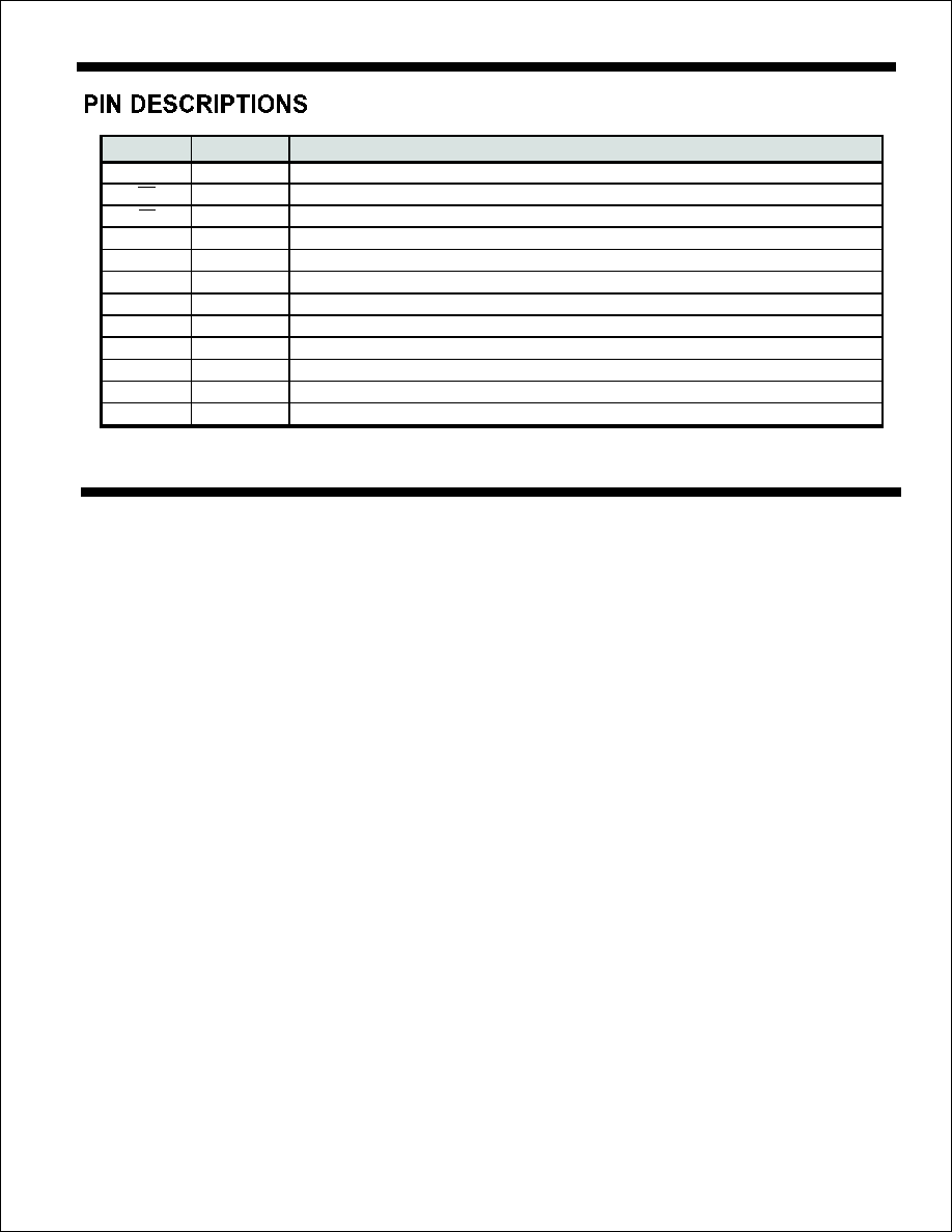
SYMBOL
FUNCTION
DESCRIPTION
VSS
POWER
0 Volts
INPUT
Logic input
Chip select
INPUT
Logic input
Clocks shift register on negative edge and DOUT pins on positive edge
LD
INPUT
Logic input
Segment outputs equal shift register data if Load is high
DIN
INPUT
Logic input
Shift register data input
LCD0
INPUT
Analog input
Display clock input and is always bonded out. Can swing from VEE to VDD
LCD0OPT
OUTPUT
Analog output
Bonded out only if an RC oscillator is required
VDD
POWER
5 Volts
VEE
POWER
O Volts to -30 Volts
DOUT
OUTPUT
Logic output
Selected pinout can provide shift register taps at positions 30, 32, 34, or 38
BP
OUTPUT
Display drive output
Low resistance drive for the backplane and swings from VDD to VEE
Segments
OUTPUT
Display drive output
High resistance drive for each segment and swings from VDD to VEE
CS
CL
HOLT INTEGRATED CIRCUITS
3-8

Package Type:
PIN NO. 1 IDENT
.045 x 45∞
.050
±
.005
(1.27
±
.127)
.045 x 45∞
PIN NO. 1
44-PIN PLASTIC PLCC
SEE DETAIL
A
.172
±
.008
(4.369
±
.203)
DETAIL A
.020 MIN
(.508
)
.025
.045
R
.690
±
.005
(17.526
±
.127)
SQ.
.610
±
.020
(15.494
±
.508)
.031
±
.005
(.787
±
.127)
.653
±
.004
(16.586
±
.102)
SQ.
.017
±
.004
(.432
±
.102)
.015 ± .002
(.381
±
.051)
.009
.011
44J
HI-8010/HI-8110 PACKAGE DIMENSIONS
inches (millimeters)
Package Type:
.008
(0.20)
Min.
0
∞
7
∞
ETAIL
D
A
See Detail A
.088
±
.032
(1.6
±
.175)
Typ.
.394
±
.004
(10.00
±
.10)
SQ.
.079
±
.002
(2.00
±
.05)
.092
±
.004
(2.32
±
.12)
.009 R typ
(0.23 R typ)
.012
±
.003
(.30
±
.08)
.0256 BSC
(0.65 BSC)
.009
±
.003R
(.225
±
.075R)
.035
±
.006
(.88
±
.15)
.520
±
.010
(13.2
±
.25)
SQ.
52PQS
52-PIN PLASTIC QUAD FLAT PACK
HOLT INTEGRATED CIRCUITS
1

ACKAGE
YPE
P
T
:
Package Type:
.484 ± .009
(12.294
±
.228)
SQ.
PIN 1 IDENT.
PIN 1 IDENT.
.020
±
.003
(.508
±
.076)
.085 MAX.
(2.159 MAX.)
.044
±
.011
(1.118
±
.280)
.040
± .
003
(1.016
±
.076)
40-PIN CERAMIC LEADLESS CHIP CARRIER
40S
PIN 1 IDENT.
PIN 1 IDENT.
.040 TYP.
(1.016 TYP.)
.020 TYP.
(.508 TYP.)
.090 MAX.
(2.286 MAX.)
.563
±
.009
(14.300
±
.228)
SQ.
.040
±
.007
(1.016
±
.178)
48-PIN CERAMIC LEADLESS CHIP CARRIER
48S
HI-8010/HI-8110 PACKAGE DIMENSIONS
inches (millimeters)
HOLT INTEGRATED CIRCUITS
2