
HI-8584
Enhanced ARINC 429
Serial Transmitter and Dual Receiver
PIN CONFIGURATION
(Top View)
52 - Pin Plastic Quad Flat Pack (PQFP)
(See page 13 for additional pin configuration)
HI-8584PQI
&
HI-8584PQT
52
-
51
-
RIN2B
50
-
RIN2A
49
-
RIN1B
48
-
RIN1A
47
-
VDD
46
-
N/C
45
-
N/C
44
-
43
-
TXCLK
42
-
CLK
41
-
40
-
N/C
D/R1
MR
RSR
39 - N/C
38 -
37 - ENTX
36 - N/C
35 -
34 - 429DO
33 - N/C
32 -
31 -
30 - TX/R
29 -
28 -
27 - BD00
CWSTR
FFT
HFT
PL2
PL1
429DO
BD10
-
14
BD09
-
15
BD08
-1
6
BD07
-1
7
BD06
-1
8
N/C
-1
9
VSS
-2
0
-2
1
BD05
-2
2
BD04
-2
3
BD03
-
24
BD02
-2
5
BD01
-2
6
NFD
FF1
HF1
D/R2
FF2
HF2
EN1
EN2
- 1
- 2
- 3
- 4
- 5
SEL - 6
- 7
- 8
BD15 - 9
BD14 - 10
BD13 - 11
BD12 - 12
BD11 - 13
GENERAL DESCRIPTION
The HI-8584 from Holt Integrated Circuits is a silicon gate
CMOS device for interfacing a 16-bit parallel data bus to the
ARINC 429 serial bus. The HI-8584 design offers many
enhancements to the industry standard HI-8282
architecture. The device provides two receivers each with
label recognition, a 32 by 32 FIFO, and an analog line
receiver. Up to 16 labels may be programmed for each
receiver. The independent transmitter also has a 32 by 32
FIFO The status of all three FIFOs can be monitored using
the external status pins or by polling the HI-8584's status
register.
Other new features include a programmable option of data
or parity in the 32nd bit, and the ability to unscramble the 32
bit word. Also, versions are available with different values
of input resistance to allow users to more easily add
external lightning protection circuitry. The device can be
used at nonstandard data rates when an option pin,
, is
invoked.
The 16-bit parallel data bus exchanges the 32-bit ARINC
data word in two steps when either loading the transmitter
or interrogating the receivers. The databus and all control
signals are CMOS and TTL compatible.
The HI-8584 applies the ARINC protocol to the receivers
and transmitter. Timing is based on a 1 Megahertz clock.
NFD
.
Additional interface circuitry such as the Holt HI-8585,
HI-8586 or HI-3182 is required to translate the transmit-
ter's 5 volt logic outputs to ARINC 429 drive levels.
APPLICATIONS
!
!
!
Avionics data communication
Serial to parallel conversion
Parallel to serial conversion
FEATURES
!
!
!
!
!
!
!
!
!
!
ARINC specification 429 compatible
Dual receiver and transmitter interface
Programmable label recognition
32 x 32 FIFOs each receiver and transmitter
Status register
Data scramble control
32nd transmit bit can be data or parity
Self test mode
Low power
Industrial & full military temperature ranges
!
!
!
Analog line receivers connect directly to
ARINC bus
On-chip 16 label memory for each receiver
Independent data rate selection for
transmitter and each receiver
HOLT INTEGRATED CIRCUITS
www.holtic.com
(DS8584 Rev. A)
02/03
February 2003

SIGNAL
FUNCTION
DESCRIPTION
VDD
POWER
+5V ± %
BD05
I/O
Data Bus
BD04
I/O
Data Bus
BD03
I/O
Data Bus
BD02
I/O
Data Bus
5
RIN1A
INPUT
ARINC receiver 1 positive input
RIN1B
INPUT
ARINC receiver 1 negative input
RIN2A
INPUT
ARINC receiver 2 positive input
RIN2B
INPUT
ARINC receiver 2 negative input
OUTPUT
Receiver 1 data ready flag
OUTPUT
FIFO full Receiver 1
OUTPUT
FIFO Half full, Receiver 1
OUTPUT
Receiver 2 data ready flag
OUTPUT
FIFO full Receiver 2
OUTPUT
FIFO Half full, Receiver 2
SEL
INPUT
Receiver data byte selection (0 = BYTE 1) (1 = BYTE 2)
INPUT
Data Bus control, enables receiver 1 data to outputs
INPUT
Data Bus control, enables receiver 2 data to outputs if
is high
BD15
I/O
Data Bus
BD14
I/O
Data Bus
BD13
I/O
Data Bus
BD12
I/O
Data Bus
BD11
I/O
Data Bus
BD10
I/O
Data Bus
BD09
I/O
Data Bus
BD08
I/O
Data Bus
BD07
I/O
Data Bus
BD06
I/O
Data Bus
GND
POWER
0 V
BD01
I/O
Data Bus
BD00
I/O
Data Bus
INPUT
Latch enable for byte 1 entered from data bus to transmitter FIFO.
INPUT
Latch enable for byte 2 entered from data bus to transmitter FIFO. Must follow
TX/R
OUTPUT
Transmitter ready flag. Goes low when ARINC word loaded into FIFO. Goes high
after transmission and FIFO empty.
OUTPUT
Transmitter FIFO Half Full
OUTPUT
Transmitter FIFO Full
429DO
OUTPUT
"ONES" data output from transmitter
OUTPUT
"ZEROS" data output from transmitter
ENTX
INPUT
Enable Transmission
INPUT
Clock for control word register
INPUT
Read Status Register if SEL=0, read Control Register if SEL=1
INPUT
No frequency discrimination if low (pull-up)
CLK
INPUT
Master Clock input
TX CLK
OUTPUT
Transmitter Clock equal to Master Clock (CLK), divided by either 10 or 80.
INPUT
Master Reset, active low
D/R1
FF1
HF1
D/R2
FF2
HF2
EN1
EN2
EN1
PL1
PL2
PL1.
HFT
FFT
429DO
CWSTR
RSR
NFD
MR
PIN DESCRIPTIONS
HOLT INTEGRATED CIRCUITS
2
HI-8584

SR
Bit
FUNCTION
STATE
DESCRIPTION
SR0
Data ready
0
Receiver 1 FIFO empty
1
Receiver 1 FIFO contains valid data
Resets to zero when all data has
been read.
pin is the inverse of
this bit
(Receiver 1)
SR1
FIFO half full
0
Receiver 1 FIFO holds less than 16
(Receiver 1)
words
1
Receiver 1 FIFO holds at least 16
words.
pin is the inverse of
this bit.
SR2
FIFO full
0
Receiver 1 FIFO not full
(Receiver 1)
1
Receiver 1 FIFO full. To avoid data
loss, the FIFO must be read within
one ARINC word period.
pin is
the inverse of this bit
SR3
Data ready
0
Receiver 2 FIFO empty
(Receiver 2)
1
Receiver 2 FIFO contains valid data
Resets to zero when all data has
been read.
pin is the inverse of
this bit
SR4
FIFO half full
0
Receiver 2 FIFO holds less than 16
(Receiver 2)
words
1
Receiver 2 FIFO holds at least 16
words.
pin is the inverse of
this bit.
SR5
FIFO full
0
Receiver 2 FIFO not full
(Receiver 2)
1
Receiver 2 FIFO full. To avoid data
loss, the FIFO must be read within
one ARINC word period.
pin is
the inverse of this bit
SR6
Transmitter FIFO
0
Transmitter FIFO not empty
empty
1
Transmitter FIFO empty.
SR7
Transmitter FIFO
0
Transmitter FIFO not full
full
1
Transmitter FIFO full.
pin is the
inverse of this bit.
SR8
Transmitter FIFO
0
Transmitter FIFO contains less than
half full
16 words
1
Transmitter FIFO contains at least
16 words.
pin is the
inverse of this bit.
D/R1
HF1
FF1
D/R2
HF2
FF2
FFT
HFT
FUNCTIONAL DESCRIPTION
CONTROL WORD REGISTER
The HI-8584 contains a 16-bit control register which is used to con-
figure the device. The control register bits CR0 - CR15 are loaded
from BD00 - BD15 when
is pulsed low. The control regis-
ter contents are output on the databus when SEL = 1 and
is
pulsed low. Each bit of the control register has the following func-
tion:
CWSTR
RSR
STATUS REGISTER
The HI-8584 contains a 9-bit status register which can be interro-
gated to determine the status of the ARINC receivers, data FIFOs
and transmitter. The contents of the status register are output on
BD00 - BD08 when the
pin is taken low and SEL = 0. Unused
bits are output as zeros. The following table defines the status reg-
ister bits.
RSR
HOLT INTEGRATED CIRCUITS
3
HI-8584
CR
Bit
FUNCTION
STATE
DESCRIPTION
CR0
Receiver 1
0
Data rate = CLK/10
Select
1
Data rate = CLK/80
Data clock
CR1
Label Memory
0
Normal operation
Read / Write
1
Load 16 labels using
/
Read 16 labels using
/
CR2
Enable Label
0
Disable label recognition
Recognition
(Receiver 1)
1
Enable label recognition
CR3
Enable Label
0
Disable Label Recognition
Recognition
(Receiver 2)
1
Enable Label recognition
CR4
Enable
0
Transmitter 32nd bit is data
32nd bit
as parity
1
Transmitter 32nd bit is parity
CR5
Self Test
0
The 429DO and
digital
outputs are internally connected
to the receiver logic inputs
1
Normal operation
CR6
Receiver 1
0
Receiver 1 decoder disabled
decoder
1
ARINC bits 9 and 10 must match
CR7 and CR8
CR7
-
-
If receiver 1 decoder is enabled,
the ARINC bit 9 must match this bit
CR8
-
-
If receiver 1 decoder is enabled,
the ARINC bit 10 must match this bit
CR9
Receiver 2
0
Receiver 2 decoder disabled
Decoder
1
ARINC bits 9 and 10 must match
CR10 and CR11
CR10
-
-
If receiver 2 decoder is enabled,
the ARINC bit 9 must match this bit
CR11
-
-
If receiver 2 decoder is enabled,
the ARINC bit 10 must match this bit
CR12
Invert
0
Transmitter 32nd bit is Odd parity
Transmitter
parity
1
Transmitter 32nd bit is Even parity
CR13
Transmitter
0
Data rate=CLK/10, O/P slope=1.5us
data clock
select
1
Data rate=CLK/80, O/P slope=10us
CR14
Receiver 2
0
Data rate=CLK/10
data clock
select
1
Data rate=CLK/80
CR15
Data
0
Scramble ARINC data
format
1
Unscramble ARINC data
PL1 PL2
EN1 EN2
429DO

v
cc
GND
GND
RIN1B
OR
RIN2B
RIN1A
OR
RIN2A
DIFFERENTIAL
AMPLIFIERS
ONES
COMPARATORS
NULL
ZEROES
v
cc
FIGURE 1. ARINC RECEIVER INPUT
The HI-8584 guarantees recognition of these levels with a common
mode Voltage with respect to GND less than ±4 for the worst case
condition (4.75V supply and 13V signal level).
The tolerances in the design guarantee detection of the above
levels, so the actual acceptance ranges are slightly larger. If the
ARINC signal is out of the actual acceptance ranges, including the
nulls, the chip rejects the data.
RECEIVER LOGIC OPERATION
BIT TIMING
BIT RATE
PULSE RISE TIME
PULSE FALL TIME
PULSE WIDTH
Figure 2 shows a block diagram of the logic section of each receiver.
The ARINC 429 specification contains the following timing specifi-
cation for the received data:
100K BPS ± 1% 12K -14.5K BPS
1.5 ± 0.5 µsec
10 ± 5 µsec
1.5 ± 0.5 µsec
10 ± 5 µsec
5 µsec ± 5%
34.5 to 41.7 µsec
If the
pin is high, the HI-8584 accepts signals that meet these
specifications and rejects outside the tolerances.
The way the
logic operation achieves this is described below:
HIGH SPEED
LOW SPEED
NFD
3. Each data bit must follow its predecessor by not less than
8 samples and no more than 12 samples. In this manner the
bit rate is checked. With exactly 1MHz input clock frequency,
the acceptable data bit rates are as follows:
83K BPS
10.4K BPS
125K BPS
15.6K BPS
4. The Word Gap timer samples the Null shift register every
10 input clocks (80 for low speed) after the last data bit of a
valid reception. If the Null is present, the Word Gap counter is
incremented. A count of 3 will enable the next reception.
If
is held low, frequency discrimination is disabled and any
data stream totaling 32 bits is accepted even with gaps between
bits. The protocol still requires a word gap as defined in 4. above.
HIGH SPEED
LOW SPEED
DATA BIT RATE MIN
DATA BIT RATE MAX
NFD
FUNCTIONAL DESCRIPTION (cont.)
THE RECEIVERS
ARINC BUS INTERFACE
Figure 1 shows the input circuit for each receiver. The ARINC 429
specification requires the following detection levels:
ONE
+6.5 Volts to +13 Volts
NULL
+2.5 Volts to -2.5 Volts
ZERO
-6.5 Volts to -13 Volts
STATE
DIFFERENTIAL VOLTAGE
1. Key to the performance of the timing checking logic is an
accurate 1MHz clock source. Less than 0.1% error is recom-
mended.
2. The sampling shift registers are 10 bits long and must
show three consecutive Ones, Zeros or Nulls to be consid-
ered valid data. Additionally, for data bits, the One or Zero in
the upper bits of the sampling shift registers must be followed
by a Null in the lower bits within the data bit time. For a Null in
the word gap, three consecutive Nulls must be found in both
the upper and lower bits of the sampling shift register.
In this
manner the minimum pulse width is guaranteed.
HOLT INTEGRATED CIRCUITS
4
HI-8584
ARINC 429 DATA FORMAT
Control register bit CR15 is used to control how individual bits in the
received or transmitted ARINC word are mapped to the HI-8584
data bus during data read or write operations. The following table
describes this mapping:
DATA
BD BD BD BD BD BD BD BD BD BD BD BD BD BD BD BD
BUS
15
14
13
12
11
10
09
08
07
06
05
04
03
02
01
00
ARINC
13
12
11
10
9
31
30
32
1
2
3
4
5
6
7
8
BIT
CR15=0
BYTE 1
ARINC
16
15
14
13
12
11
10
9
8
7
6
5
4
3
2
1
BIT
CR15=1
BYTE 2
DATA
BD BD BD BD BD BD BD BD BD BD BD BD BD BD BD BD
BUS
15
14
13
12
11
10
09
08
07
06
05
04
03
02
01
00
ARINC
29
28
27
26
25
24
23
22
21
20
19
18
17
16
15
14
BIT
CR15=0
ARINC
32
31
30
29
28
27
26
25
24
23
22
21
20
19
18
17
BIT
CR15=1
Parity
SDI
SDI
Label
Label
SDI
SDI
Label
Label
Label
Label
Label
Label
Label
Label
Label
Label
Label
Label
Label
Label
Parity

FIFO
LOAD
CONTROL
SEL
EN
CONTROL
BIT
/
R/W
CONTROL
32 TO 16 DRIVER
32 BIT SHIFT REGISTER
TO PINS
CONTROLBITS
CR0, CR14
CLOCK
OPTION
CLOCK
CLK
BIT
COUNTER
AND
END OF
SEQUENCE
PARITY
CHECK
32ND
BIT
DATA
BIT CLOCK
WORD GAP
WORD GAP
TIMER
BIT CLOCK
END
START
SEQUENCE
CONTROL
ERROR
CLOCK
ERROR
DETECTION
SHIFT REGISTER
SHIFT REGISTER
NULL
ZEROS
SHIFT REGISTER
ONES
EOS
FIGURE 2.
RECEIVER BLOCK DIAGRAM
LABEL /
DECODE
COMPARE
16 x 8
LABEL
MEMORY
32 X 32
FIFO
D/R
FF
MUX
CONTRO
L
CONTROL
BITS
HF
FUNCTIONAL DESCRIPTION (cont.)
0
X
0
X
Load FIFO
1
No
0
X
Ignore data
1
Yes
0
X
Load FIFO
0
X
1
No
Ignore data
0
X
1
Yes
Load FIFO
1
Yes
1
No
Ignore data
1
No
1
Yes
Ignore data
1
No
1
No
Ignore data
1
Yes
1
Yes
Load FIFO
CR2(3) ARINC word CR6(9) ARINC word
FIFO
matches
bits 9,10
label
match
CR7,8 (10,11)
RECEIVER PARITY
The receiver parity circuit counts Ones received, including the
parity bit. If the result is odd, then "0" will appear in the 32nd bit.
RETRIEVING DATA
Once 32 valid bits are recognized, the receiver logic generates an
End of Sequence (EOS). Depending upon the state of control
register bits CR2-CR11, the received ARINC 32-bit word is then
checked for correct decoding and label matching before being
loaded into the 32 x 32 receive FIFO. ARINC words which do not
meet the necessary 9th and 10th ARINC bit or label matching are
ignored and are not loaded into the receive FIFO. The following
table describes this operation.
HOLT INTEGRATED CIRCUITS
5
HI-8584

FUNCTIONAL DESCRIPTION (cont.)
READING LABELS
After the write that changes CR1 from 0 to 1, the next 16 data
reads of the selected receiver (
taken low) are labels.
is
used to read labels for receiver 1, and
to read labels for
receiver 2. Label data is presented on BD00 - BD07.
When writing to, or reading from the label memory, SEL must be a
one, all 16 locations should be accessed, and CR1 must be
written to zero before returning to normal operation. Label
recognition must be disabled (CR2/3=0) during the label read
sequence.
EN
EN1
EN2
TRANSMITTER
FIFO OPERATION
The FIFO is loaded sequentially by first pulsing
to load byte 1
and then
to load byte 2. The control logic automatically loads
the 31 bit word (or 32 bit word if CR4=0) in the next available
position of the FIFO. If TX/R, the transmitter ready flag is high
(FIFO empty), then up to 32 words, each 31 or 32 bits long, may
be loaded. If TX/R is low, then only the available positions may be
loaded. If all 32 positions are full, the
flag is asserted and the
FIFO ignores further attempts to load data.
A transmitter FIFO half-full flag
is provided. When the
transmit FIFO contains less than 16 words,
is high,
indicating to the system microprocessor that a 16 ARINC word
block write sequence can be initiated.
In normal operation (CR4=1), the 32nd bit transmitted is a parity
bit. Odd or even parity is selected by programming control
register bit CR12 to a zero or one. If CR4 is programmed to a 0,
then all 32-bits of data loaded into the transmitter FIFO are treated
as data and are transmitted.
PL1
PL2
FFT
HFT
HFT
CR4,12
FIGURE 3.
TRANSMITTER BLOCK DIAGRAM
DATA
CLOCK
CR13
PL1
PL2
CLK
TX CLK
PARITY
GENERATOR
DATA AND
NULL TIMER
SEQUENCER
BIT
AND
WORD GAP
COUNTER
START
SEQUENCE
WORD COUNTER
AND
FIFO CONTROL
INCREMENT
WORD COUNT
DATA CLOCK
DIVIDER
FIFO
LOADING
SEQUENCER
429DO
429DO
32 x 32 FIFO
32 BIT PARALLEL
LOAD SHIFT REGISTER
BIT CLOCK
WORD CLOCK
ADDRESS
LOAD
DATA BUS
TX/R
ENTX
The chip compares the incoming label to the stored labels if label
recognition is enabled. If a match is found, the data is processed.
If a match is not found, no indicators of receiving ARINC data are
presented. Note that 00(Hex) is treated in the same way as any
other label value. Label bit significance is not changed by the
status of control register bit CR15. Label bits BD00-BD07 are
always compared to received ARINC bits 1 -8 respectively.
After a write that takes CR1 from 0 to 1, the next 16 writes of data
(
pulsed low) load label data into each location of the label
memory from the BD00 - BD07 pins. The
pin is used to write
label data for receiver 1 and
for receiver 2.
LOADING LABELS
PL
PL1
PL2
Note that ARINC
word reception is suspended during the label memory write
sequence.
Once a valid ARINC word is loaded into the FIFO, then EOS
clocks the data ready flag flip flop to a "1",
or
(or both)
will go low. The data flag for a receiver will remain low until
ARINC bytes from that receiver are retrieved and the FIFO is
empty. This is accomplished by first activating
with SEL, the
byte selector, low to retrieve the first byte and then activating
with SEL high to retrieve the second byte.
retrieves data
from receiver 1 and
retrieves data from receiver 2.
Up to 32 ARINC words may be loaded into each receiver's FIFO.
The
(
) pin will go low when the receiver 1 (2) FIFO is full.
Failure to retrieve data from a full FIFO will cause the next valid
ARINC word received to overwrite the existing data in FIFO
location 32. A FIFO half full flag
(
) goes low if the FIFO
contains 16 or more received ARINC words. The
(
) pin is
intended to act as an interrupt flag to the system's external
microprocessor, allowing a 16 word data retrieval routine to be
performed, without the user needing to continually poll the HI-
8584's status register bits.
D/R1
D/R2
EN
EN
EN1
EN2
FF1 FF2
HF1 HF2
HF1 HF2
both
LABEL RECOGNITION
HOLT INTEGRATED CIRCUITS
6
HI-8584
HFT
FFT

The word counter detects when all loaded positions have been
transmitted and sets the transmitter ready flag, TX/R, high.
TRANSMITTER PARITY
SELF TEST
SYSTEM OPERATION
The parity generator counts the Ones in the 31-bit word.
If
control register bit CR12 is set low, the 32nd bit transmitted will
make parity odd. If the control bit is, high the parity is even.
Setting CR4 to a Zero bypasses the parity generator, and allows
32 bits of data to be transmitted.
If control register bit CR5 is set low, the transmitter serial output
data are internally connected to each of the two receivers,
bypassing the analog interface circuitry. Data is passed
unmodified to receiver 1 and inverted to receiver 2. The serial
data from the transmitter is always present on the 429DO and
outputs regardless of the state of CR5.
The two receivers are independent of the transmitter. There-
fore, control of data exchanges is strictly at the option of the
user. The only restrictions are:
1. The received data will be overwritten if the receiver
FIFO is full and at least one location is not retrieved before
the next complete ARINC word is received.
2. The transmitter FIFO can store 32 words maximum and
ignores attempts to load additional data if full.
429DO
REPEATER OPERATION
Repeater mode of operation allows a data word that has been
received by the HI-8584 to be placed directly into the transmitter
FIFO. Repeater operation is similar to normal receiver operation.
In normal operation, either byte of a received data word may be
read from the receiver latches first by use of SEL input. During
repeater operation however, the lower byte of the data word must
be read first. This is necessary because, as the data is being read,
it is also being loaded into transmitter FIFO which is always loaded
with the lower byte of the data word first. Signal flow for repeater
operation is shown in the Timing Diagrams section.
Please refer to the Holt AN-300 Application Note for additional
information and recommendations on lightning protection of Holt
line drivers and line receivers.
HI-8584-10
The HI-8584-10 option is similar to the HI-8584 with the exception
that it allows an external 10 Kohm resistor to be added in series
with each ARINC input without affecting the ARINC input thresh-
olds. This option is especially useful in applications where light-
ning protection circuitry is also required.
Each side of the ARINC bus must be connected through a 10 Kohm
series resistor in order for the chip to detect the correct ARINC
levels. The typical 10 volt differential signal is translated and input
to a window comparator and latch. The comparator levels are set
so that with the external 10 Kohm resistors, they are just below the
standard 6.5 volt minimum ARINC data threshold and just above
the standard 2.5 volt maximum ARINC null threshold.
The HI-8584 may be operated at clock frequencies beyond that re-
quired for ARINC compliant operation. For operation at Master
Clock (CLK) frequencies up to 5MHz, please contact Holt applica-
tions engineering.
HIGH SPEED OPERATION
FUNCTIONAL DESCRIPTION (cont.)
DATA TRANSMISSION
When ENTX goes high, enabling transmission, the FIFO
positions are incremented with the top register loading into the
data transmission shift register. Within 2.5 data clocks the first
data bit appears at 429DO and
. The 31 or 32 bits in the
data transmission shift register are presented sequentially to the
outputs in the ARINC 429 format with the following timing:
429DO
ARINC DATA BIT TIME
10 Clocks
80 Clocks
DATA BIT TIME
5 Clocks
40 Clocks
NULL BIT TIME
5 Clocks
40 Clocks
WORD GAP TIME
40 Clocks
320 Clocks
HIGH SPEED
LOW SPEED
HOLT INTEGRATED CIRCUITS
7
HI-8584

DATA RATE - EXAMPLE PATTERN
429 DATA
ARINC BIT
429 DATA
NULL
DATA
DATA
DATA
NULL
NULL
WORD GAP
BIT 1
NEXT WORD
BIT 32
BIT 31
BIT 30
TRANSMITTER OPERATION
PL2
DWSET
t
DWHLD
t
TX/R
t
DWHLD
t
PL12
t
PL
t
DATA BUS
PL1
TX/R,
,
HFT FFT
BYTE 2 VALID
PL
t
PL12
t
DWSET
t
BYTE 1 VALID
SELEN
t
ENSEL
t
SELEN
t
BYTE 1
DATAEN
t
ENDATA
t
READEN
t
RECEIVER OPERATION
D/R HF FF
,
,
ARINC DATA
SEL
EN
DATA BUS
BIT 31
BIT 32
SELEN
t
D/R
t
DATAEN
t
D/REN
t
END/R
t
EN
t
ENSEL
t
ENDATA
t
ENDATA
t
ENEN
t
DON'T CARE
BYTE 1 VALID
BYTE 2 VALID
LOADING CONTROL WORD
CWHLD
t
CWSET
t
CWSTR
t
DATA BUS
CWSTR
VALID
TIMING DIAGRAMS
HOLT INTEGRATED CIRCUITS
8
HI-8584

TIMING DIAGRAMS
STATUS REGISTER READ CYCLE
BYTE SELECT
SEL
RSR
DATA BUS
SELEN
t
DATAEN
t
ENSEL
t
ENDATA
t
DON'T CARE
DON'T CARE
DATA VALID
HOLT INTEGRATED CIRCUITS
9
HI-8584
CONTROL REGISTER READ CYCLE
BYTE SELECT
SEL
RSR
DATA BUS
SELEN
t
DATAEN
t
ENSEL
t
ENDATA
t
DON'T CARE
DON'T CARE
DATA VALID
LABEL MEMORY LOAD SEQUENCE
CWSTR
/
PL1 PL2
DATA BUS
Set CR1=1
Label #1
Label #2
Label #16
Set CR1=0
CWSTR
t
CWSET
t
CWHLD
t
DWSET
t
DWHLD
t
PL
t
LABEL MEMORY READ SEQUENCE
CWSTR
/
EN1 EN2
DATA BUS
Set CR1=1
Label #1
Label #16
Set CR1=0
CWSTR
t
CWSET
t
CWHLD
t
ENDATA
t
Label #2
DATAEN
t
LABEL
t
READEN
t

REPEATER OPERATION TIMING
DON'T CARE
RIN
D/R
EN
PL1
PL2
SEL
TXR
ENTX
429DO
429DO
BIT 32
DON'T CARE
D/R
t
EN
t
D/REN
t
ENEN
t
EN
t
END/R
t
SELEN
t
ENSEL
t
ENPL
t
PLEN
t
SELEN
t
ENSEL
t
ENPL
t
PLEN
t
TX/R
t
TX/REN
t
ENDAT
t
ENTX/R
t
DTX/R
t
NULL
t
BIT 1
BIT 32
One
Zero
Null
TIMING DIAGRAMS (cont.)
HOLT INTEGRATED CIRCUITS
10
HI-8584
TRANSMITTING DATA
ARINC BIT
PL2
ENTX
429DO
429DO
TXR
PL2EN
t
ENDAT
t
DTX/R
t
ENTX/R
t
DATA
BIT 2
ARINC BIT
DATA
BIT 32
Null
One
Null
ARINC BIT
DATA
BIT 1

LIMITS
PARAMETER
CONDITIONS
UNIT
SYMBOL
Differential Input Voltage:
ONE
V
Common mode voltage
6.5
10.0
13.0
V
(RIN1A to RIN1B, RIN2A to RIN2B)
ZERO
V
less than ±4V with
-13.0
-10.0
-6.5
V
NULL
V
with respect to GND
-2.5
0
2.5
V
Input Resistance:
Differential
R
12
46
K
To GND
R
12
38
K
To V
R
12
38
K
Input Current:
Input Sink
I
200
µA
Input Source
I
-450
µA
Input Capacitance:
Differential
C
20
pF
(Guaranteed but not tested)
To GND
C
20
pF
To V
C
20
pF
Input Voltage:
Input Voltage HI
V
2.0
V
Input Voltage LO
V
0.8
V
Input Current:
Input Sink
I
1.5
µA
Input Source
I
-1.5
µA
Input Voltage:
Input Voltage HI
V
2.0
V
Input Voltage LO
V
0.8
V
Input Current:
Input Sink
I
1.5
µA
Input Source
I
-1.5
A
Pull-up current (
Pin)
I
-150
-50
MIN
TYP
MAX
ARINC INPUTS
-
Pins RIN1A, RIN1B, RIN2A, RIN2B
BI-DIRECTIONAL INPUTS - Pins BD00 - BD15
OTHER INPUTS
IH
IL
NUL
I
G
DD
H
IH
IL
I
G
DD
H
IH
IL
IH
IL
IH
IL
IH
IL
PU
W
NFD
W
W
(RIN1A to RIN1B, RIN2A to RIN2B)
µ
µA
Output Voltage:
Logic "1" Output Voltage
V
I
= -1.0mA
2.7
V
Logic "0" Output Voltage
V
I
= 1.6mA
0.4
V
Output Current:
Output Sink
I
V
= 0.4V
1.6
mA
(Bi-directional Pins)
Output Source
I
V
= V
- 0.4V
-1.0
mA
Output Current:
Output Sink
I
V
= 0.4V
1.6
mA
(All Other Outputs)
Output Source
I
V
= V
- 0.4V
-1.0
mA
Output Capacitance:
C
15
pF
VDD
I
4
20
mA
OUTPUTS
Operating Supply Current
OH
OH
OL
OL
OL
OUT
OH
OUT
DD
OL
OUT
OH
OUT
DD
O
DD
Supply Voltages V
........................................... -0.3V to +7V
Voltage at pins RIN1A, RIN1B, RIN2A, RIN2B ..... -29V to +29V
Voltage at any other pin ............................... -0.3V to V
+0.3V
Solder temperature (Leads) .................... 280
for 10 seconds
(Package) .......................................... 220
DD
DD
∞C
∞C
Power Dissipation at 25∞C .......................................... 500 mW
DC Current Drain per pin .............................................. ±10mA
Operating Temperature Range (Industrial): .... -40∞C to +85∞C
(Military): ..... -55∞C to +125∞C
Storage Temperature Range ........................ -65∞C to +150∞C
ABSOLUTE MAXIMUM RATINGS
NOTE: Stresses above those listed under "Absolute Maximum Ratings" may cause permanent damage to the device. These are stress ratings only.
Functional operation of the device at these or any other conditions above those indicated in the operational sections of the specifications is not implied.
Exposure to absolute maximum rating conditions for extended periods may affect device reliability.
DC ELECTRICAL CHARACTERISTICS
V
= 5V , GND = 0V, TA = Operating Temperature Range (unless otherwise specified).
DD
HOLT INTEGRATED CIRCUITS
11
HI-8584
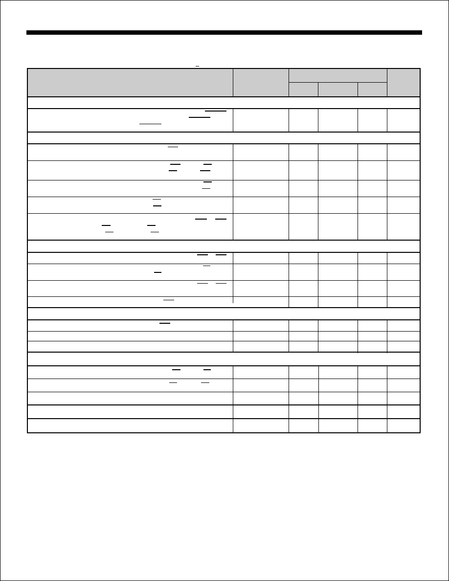
AC ELECTRICAL CHARACTERISTICS
VDD = 5V, GND = 0V, TA = Oper. Temp. Range and fclk=1MHz 0.1% with 60/40 duty cycle
+
LIMITS
PARAMETER
SYMBOL
UNITS
MIN
TYP
MAX
CONTROL WORD TIMING
RECEIVER FIFO AND LABEL READ TIMING
TRANSMITTER FIFO AND LABEL WRITE TIMING
TRANSMISSION TIMING
Pulse Width -
t
80
ns
Setup - DATA BUS Valid to
HIGH
t
50
ns
Hold -
HIGH to DATA BUS Hi-Z
t
0
ns
Delay - Start ARINC 32nd Bit to
LOW: High Speed
t
16
µs
Low Speed
t
128
µs
Delay -
LOW to
LOW
t
0
ns
Delay -
LOW to
HIGH
t
250
350
ns
Setup - SEL to
LOW
t
10
ns
Hold - SEL to
HIGH
t
10
ns
Delay -
LOW to DATA BUS Valid
t
60
100
ns
Delay -
HIGH to DATA BUS Hi-Z
t
50
80
ns
Pulse Width -
or
t
60
ns
Spacing -
HIGH to next
LOW (Same ARINC Word)
t
60
ns
Spacing -
HIGH to next
LOW (Next ARINC Word)
t
200
ns
Pulse Width -
or
t
80
ns
Setup - DATA BUS Valid to
HIGH
t
50
ns
Hold -
HIGH to DATA BUS Hi-Z
t
10
ns
Spacing -
or
t
85
ns
Spacing between Label Write pulses
t
200
ns
Delay -
HIGH to TX/R LOW
t
300
ns
Spacing -
HIGH to ENTX HIGH
t
0
µs
Delay - 32nd ARINC Bit to TX/R HIGH
t
50
ns
Spacing - TX/R HIGH to ENTX LOW
t
0
ns
CWSTR
CWSTR
CWSTR
D/R
D/R
EN
EN
D/R
EN
EN
EN
EN
EN1
EN2
EN
EN
EN
EN
PL1
PL2
PL
PL
PL1
PL2
PL2
PL2
CWSTR
CWSET
CWHLD
D/R
D/R
D/REN
END/R
SELEN
ENSEL
ENDATA
DATAEN
EN
ENEN
READEN
PL
DWSET
DWHLD
PL12
LABEL
TX/R
PL2EN
DTX/R
ENTX/R
HOLT INTEGRATED CIRCUITS
12
HI-8584
REPEATER OPERATION TIMING
Hold -
HIGH to
HIGH
t
0
ns
Delay - TX/R LOW to ENTX HIGH
t
0
ns
t
50
ns
± 1%
PL
EN
PLEN
TX/REN
MR
MASTER RESET PULSE WIDTH
ARINC DATA RATE AND BIT TIMING
Delay -
LOW to
LOW
t
0
ns
EN
PL
ENPL

ORDERING INFORMATION
HI-8584
ADDITIONAL HI-8584 PIN CONFIGURATION
HOLT INTEGRATED CIRCUITS
13
PACKAGE
DESCRIPTION
TEMPERATURE
RANGE
LEAD
FINISH
SOLDER
SOLDER
52 PIN PLASTIC QUAD FLAT PACK (PQFP)
52 PIN CERQUAD J LEAD
FLOW
BURN
IN
-40∞C TO +85∞C
NO
I
-55∞C TO +125∞C
NO
T
HI - 8584 xx x - xx
INPUT SERIES RESISTANCE
BUILT-IN
REQUIRED EXTERNALLY
PART
NUMBER
25 Kohm
10 Kohm
-10
35 Kohm
0
No dash number
PART
NUMBER
T
I
PART
NUMBER
PQ
CJ
7
-
6
-
RIN2B
5
-
RIN2A
4
-
RIN1B
3
-
RIN1A
2
-
VDD
1
-
N/C
52
-
N/C
51
-
50
-
TXCLK
49
-
CLK
48
-
47
-
N/C
D/R1
M
R
RSR
46 - N/C
45 -
44 - ENTX
43 - N/C
42 -
41 - 429DO
40 - N/C
39 -
38 -
37 - TX/R
36 -
35 -
34 - BD00
CWSTR
FFT
HFT
PL2
PL1
429DO
BD10
-2
1
BD09
-2
2
BD08
-2
3
BD07
-2
4
BD06
-
2
5
N/C
-2
6
VSS
-2
7
-2
8
BD05
-2
9
BD04
-
3
0
BD03
-3
1
BD02
-3
2
BD01
-3
3
NFD
FF1
HF1
D/R2
FF2
HF2
EN1
EN2
- 8
- 9
- 10
- 11
- 12
SEL - 13
- 14
-15
BD15 - 16
BD14 - 17
BD13 - 18
BD12 - 19
BD11 - 20
HI-8584CJI
&
HI-8584CJT
52 - Pin Cerquad J-lead
(See page 1 for additional pin configuration)

HI-8584 PACKAGE DIMENSIONS
inches (millimeters)
HOLT INTEGRATED CIRCUITS
14
Package Type:
.008
(0.20)
Min.
0∞ £ Q £7∞
D
A
ETAIL
See Detail A
.079 ± .002
(2.00 ± .05)
.092 ± .004
(2.32 ± .12)
.009 R typ
(0.23 R typ)
.012 ± .003
(.30 ± .08)
.0256 BSC
(0.65 BSC)
.009 ± .003R
(.225 ± .075R)
.035 ± .006
(.88 ± .15)
.063 ± .032
(1.6 ± .175)
Typ.
.394 ± .004
(10.00 ± .10) SQ.
.520 ± .010
(13.2 ± .25)
SQ.
52PQS
52-PIN PLASTIC QUAD FLAT PACK (PQFP)
Package Type: 52U
52-PIN J-LEAD CERQUAD
.019 ± .002
(.483 ± .051)
8
7
1 52
47
.788
(20.0)
MAX.
SQ.
.720 ± .010
(18.29 ± .25)
.750 ± .007
(19.05 ± .18)
.190
(4.826)MAX.
(1.02 ± .013)
.040 ± .005
.050
(1.27)
TYP.