
HI-8588-10
ARINC 429 LINE RECEIVER
DESCRIPTION
FEATURES
PIN CONFIGURATION
SUPPLY VOLTAGES
FUNCTION TABLE
RINA
GND
ROUTA
ROUTB
TESTB
TESTA
VCC
RINB
2
3
4
5
6
7
8
1
vcc
= 5.0V ± 5%
PIN
SYMBOL
FUNCTION
DESCRIPTION
VCC
SUPPLY
5 VOLT SUPPLY
TESTA
LOGIC INPUT
CMOS
RINB
ARINC INPUT
RECEIVER B INPUT
RINA
ARINC INPUT
RECEIVER A INPUT
GND
POWER
GROUND
ROUTA
LOGIC OUTPUT
RECEIVER CMOS OUTPUT A
ROUTB
LOGIC OUTPUT
RECEIVER CMOS OUTPUT B
TESTB
LOGIC INPUT
CMOS
PIN DESCRIPTION TABLE
The HI-8588-10 ARINC 429 bus interface receiver is simi-
lar to the HI-8588 with the exception that it allows an exter-
nal 10 Kohm resistor in series with each ARINC input with-
out affecting the ARINC input thresholds. The product is
especially useful in applications where lightning protection
circuitry is also required. In addition, the test inputs force
both of the outputs to zero instead open circuit. The ana-
log/digital CMOS product requires only a 5 volt supply and
is available in a SO 8 pin package.
Each side of the ARINC bus
be connected through a
10 Kohm series resistor in order for the chip to detect the
correct ARINC levels. The typical 10 volt differential signal
is translated and input to a window comparator and latch.
The comparator levels are set so that with the external
10 Kohm resistors they are just below the standard 6.5 volt
minimum ARINC data threshold and just above the stan-
dard 2.5 voltmaximum ARINC null threshold.
The TESTA and TESTB inputs bypass the analog inputs
for testing purposes. Also if TESTA and TESTB are both
taken high, the digital outputs are forced to zero.
must
January 2001
(DS8588-10 Rev. A)
01/01
HOLT INTEGRATED CIRCUITS
1
TEST
HI-8588-10
FUNCTIONAL DESCRIPTION
TXBOUT
TXAOUT
TX1IN
TX0IN
ARINC
Channel
RINB
RINA
TESTA
TESTB
{
HARDWIRE
OR
DRIVE FROM LOGIC
ROUTB
ROUTA
VCC
V-
-15V
GND
TXD0
TXD1
RXD0
RXD1
HI-6010
8 BIT BUS
ARINC
Channel
1
2
8
6
7
4
3
4
5
6
7
2
3
HI-8588-10
FIGURE 2 - APPLICATION DIAGRAM
APPLICATION INFORMATION
15V
V+
8
5
HI-8586
SLP1.5
1
RECEIVER
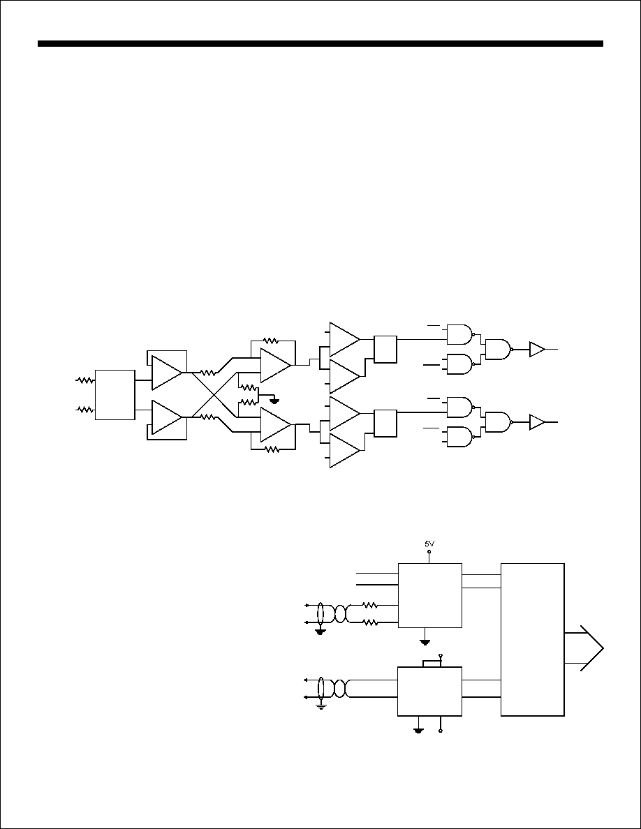
Figure 1 shows the general architecture of the ARINC 429
receiver. The receiver operates off the VCC supply only.
The inputs RINA and RINB each require 35K
of resis-
tance of which 25K
is internal to the chip. The series re-
sistance is connected to level translators whose resistance
to Ground is typically 10K . In order for the voltage trans-
lation not to be adversely affected, an external 10K
series
resister must be added to each ARINC input.
The
HI-8588-10 device is typically chosen for applications
where external series resistors are required in its lightning
protection circuitry.
After level translation, the inputs are buffered and become
inputs to a differential amplifier. The amplitude of the differ-
ential signal is compared to levels derived from a divider
W
W
W
W
Figure 2 shows a possible application of the
HI-8588 interfacing an ARINC receive channel
to the HI-6010 which in turn interfaces to an
8-bit bus.
RINA
RINB
NULL
ZERO
NULL
ONE
TESTA
ROUTB
ROUTA
FIGURE 1 - RECEIVER BLOCK DIAGRAM
S
Q
R
LATCH
ESD
PROTECTION
AND
TRANSLATION
10K
10K
between VCC and Ground. The nominal settings corre-
spond to a One/Zero amplitude of 6.0V and a Null ampli-
tude of 3.3V.
The status of the ARINC receiver input is latched. A Null
input resets the latches and a One or Zero input sets the
latches.
The logic at the output is controlled by the test signal
which is generated by the logical OR of the TestA and
TestB pins. Unlike the HI-8588, if TestA and TestB are
both One, the HI-8588-10 outputs are pulled low instead
of being tri-stated. This allows the digital outputs of a
transmitter to be connected to the test inputs through
control logic for self-test purposes.
GND
LATCH
S
Q
TESTB
R
TESTA
TESTB
TEST
HOLT INTEGRATED CIRCUITS
2

HI-8588-10
Voltages referenced to Ground
Supply voltages
VCC...................................................7V
ARINC input - pins 3 & 4
Voltage at either pin......+29V to -29V
DC current per input pin................ ±10mA
Power dissipation at 25∞C
plastic DIL............0.7W
ceramic DIL..........0.5W
Solder Temperature ........275∞C for 10 sec
Storage Temperature........-65∞C to +150∞C
ABSOLUTE MAXIMUM RATINGS
RECOMMENDED OPERATING CONDITIONS
Supply Voltages
VCC........................................5V... ± 5%
Temperature Range
Industrial Screening........-40∞C to +85∞C
Hi-Temp Screening.......-55∞C to +125∞C
Military Screening.........-55∞C to +125∞C
DC ELECTRICAL CHARACTERISTICS
PARAMETERS
SYMBOL
TEST CONDITIONS
MIN
TYP
MAX
UNITS
ARINC input voltage
one or zero
VDIN
VNIN
diff. volt. thru 10K , pins 3 & 4
W
volts
6.5
10
13
2.5
logic input voltage
high
low
V
V
ARINC input resistance
RINA to RINB
R DIFF
RINA or RINB to Gnd or VCC
R SUP
logic input current
source
sink
I
I IH
IL
null
IH
IL
logic output drive current
one
zero
I
I
OH
OL
Current drain
operating
common mode
VCOM
"
"
"
with respect to Ground
-
-
-
-
5.0
3.5
-
-
-
-
1.5
volts
volts
volts
volts
supplies floating & series 10K
W
30
19
75
40
-
-
Kohm
Kohm
"
"
"
V
VIN
IN = 5 V
= 0 V
0.1
-
-
-
-
0.1
µ
A
µ
A
V
= 4.6V
OH
V
= 0.4V
OL
-0.8
-
-1.6
5.6
3.6
mA
mA
2.3
-
6.3
mA
VCC = 5.0V UNLESS OTHERWISE STATED
OPERATING TEMPERATURE RANGE,
I
CC1
pins 2, 8 = 0V; pins 3, 4 open
NOTE:
Stresses above absolute maximum
ratings or outside recommended operating con-
ditions may cause permanent damage to the
device. These are stress ratings only. Opera-
tion at the limits is not recommended.
-
HOLT INTEGRATED CIRCUITS
3

VCC = 5.0V UNLESS OTHERWISE STATED
OPERATING TEMPERATURE RANGE,
HI-8588-10
AC ELECTRICAL CHARACTERISTICS
PARAMETERS
SYMBOL TEST CONDITIONS
MIN
TYP
MAX
UNITS
Receiver propagation delay
Output high to low
t phlr
Receiver output transition times
Output high to low
Output low to high
Output low to high
plhr
t
t fr
rr
t
ns
ns
ns
ns
Input capacitance (1)
ARINC differential
CAD
CAS
pF
ARINC single ended to Ground
Logic
C IN
pF
pF
defined in Figure 3, C = 50pF
L
V
pin 4 - pin 3
DIFF
0V
10V
-10V
5V
0V
t rr
t rr
t fr
t
10%
90%
t phlr
t
t plhr
t
5V
0V
t plhr
t
t phlr
t
pin 6
pin 7
FIGURE 3 - RECEIVER TIMING
1. Guaranteed but not tested
ORDERING INFORMATION
PART
PACKAGE
TEMPERATURE
BURN
LEAD
NUMBER
DESCRIPTION
RANGE
FLOW
IN
FINISH
HI-8588PDI-10
8 PIN PLASTIC DIP
-40∞C TO +85∞C
I
NO
SOLDER
HI-8588PDT-10
8 PIN PLASTIC DIP
-55∞C TO +125∞C
T
NO
SOLDER
HI-8588PSI-10
8 PIN PLASTIC NARROW BODY SOIC
-40∞C TO +85∞C
I
NO
SOLDER
HI-8588PST-10
8 PIN PLASTIC NARROW BODY SOIC
-55∞C TO +125∞C
T
NO
SOLDER
HI-8588CDI-10
8 PIN CERAMIC SIDE BRAZED DIP
-40∞C TO +85∞C
I
NO
GOLD
HI-8588CDT-10
8 PIN CERAMIC SIDE BRAZED DIP
-55∞C TO +125∞C
T
NO
GOLD
HI-8588CDM-10
8 PIN CERAMIC SIDE BRAZED DIP
-55∞C TO +125∞C
M
YES
SOLDER
HI-8588CRI-10
8 PIN CERDIP
-40∞C TO +85∞C
I
NO
SOLDER
HI-8588CRT-10
8 PIN CERDIP
-55∞C TO +125∞C
T
NO
SOLDER
HI-8588CRM-10
8 PIN CERDIP
-55∞C TO +125∞C
M
YES
SOLDER
HOLT INTEGRATED CIRCUITS
4

Package Type:
8-PIN PLASTIC DIP
8P
.385
±
.015
(4.699
±
.381)
7
∞
TYP.
.025
±
.010
(.635 ± .254)
.335
±
.035
(8.509
±
.889)
.250 ± .010
(6.350
±
.254)
.100
±
.010
(3.540
±
.254)
.135
±
.015
(3.429
±
.381)
.055
±
.010
(1.397
±
.254)
.1375
±
.0125
(3.493
±
.318)
.019
±
.002
(.483
±
.102)
.0115
±
.0035
(.292
±
.089)
.300
±
.010
(7.620
±
.254)
HI-8588-10 PACKAGE DIMENSIONS
inches (millimeters)
HOLT INTEGRATED CIRCUITS
5
Package Type:
Detail A
0
∞
to 8
∞
Detail A
8HN
8-PIN PLASTIC SMALL OUTLINE (SOIC) - NB
(Narrow Body)
IN
P
1
.236 ± .008
(5.994 ± .203)
.1535 ± .0035
(3.90 ± .09)
.1935 ± .0035
(4.915 ± .085)
.0086 ± .0012
(.2184 ± .0305)
.050 ± .010
(1.27 ± .254)
.033 ± .017
(.8382 ± .4318)
.055 ± .005
(1.397 ± .127)
.0069 ± .0029
(.1753 ± .0737)
.0165 ± .0035
(.4191 ± .0889)