
HI-8685, HI-8686
ARINC INTERFACE DEVICE
ARINC 429 & 561 Serial Data to 16-Bit Parallel Data
DESCRIPTION
The HI-8685 and HI-8686 are system components for
interfacing incoming ARINC 429 signals to 16-bit parallel
data using proven +5V analog/digital CMOS technology.
Both products incorporate the digital logic and analog line
receiver circuitry in a single device.
The receivers on the HI-8685 and the HI-8686 connect
directly to the ARINC 429 Bus and translate the incoming
signals to normal CMOS levels. Internal comparator levels
are set just below the standard 6.5 volt minimum data
threshold and just above the standard 2.5 volt maximum null
threshold.
The -10 version of the HI-8685 allows the
incorporation of an external 10K
resistance in series with
each ARINC input for lightning protection without affecting
ARINC level detection.
Both products offer high speed 16-bit parallel bus interface,
a 32-bit buffer, and error detection for word length and parity.
A reset pin is also provided for power-on initialization.
!
!
Automatic conversion of serial ARINC 429, 575 &
561 data to 16-bit parallel data
High speed parallel 16-bit data bus
Error detection -
and
On-chip line receiver
Input hysteresis of at least 2 volts
Test lnputs bypass analog inputs
Simplified lightning protection with the ability to add
10 Kohm external series resistors
Small,
package options:
SOIC, TQFP and PLCC
Military processing available
!
!
!
!
!
!
!
!
word length
parity
Reset input for power-on initialization
surface mount, plastic
FEATURES
PIN CONFIGURATIONS
(Top View)
February 2001
HI-8685
28-Pin Plastic SOIC - WB Package
HI-8686
32-Pin PlasticTQFP Package
HI-8686PQI
HI-8686PQT
24 -
23 - RINB-10
22 - RINB
21 - RINA
20 - RINA-10
19 - ERROR
18 - PARITY ENB
17 - N/C
RESET
HI-8685PSI
HI-8685PST
&
HI-8685PSI-10
HI-8685PST-10
DATARDY
D15
D14
D13
D12
D11
D10
D9
D8
D7
D6
D5
D4
GND
Vcc
GAPCLK
TESTA
TESTB
RINB (-10)
RINA (-10)
ERROR
PARITY ENB
D0
D1
D2
D3
RESET
READ
28
27
26
25
24
23
22
21
20
19
18
17
16
15
1
2
3
4
5
6
7
8
9
10
11
12
13
14
N/C - 1
D12 - 2
D11 - 3
D10 - 4
D9 - 5
D8 - 6
D7 - 7
D6 - 8
HOLT INTEGRATED CIRCUITS
1
(DS8685 Rev. G)
02/01
(See page 8 for additional pin configurations)

HI-8685, HI-8686
PIN DESCRIPTIONS
DATA RDY
OUTPUT
Receiver data ready flag. A high level indicates data is available in the receive
buffer. Flag goes low when the first 16-bit byte is read.
D0 to D15
OUTPUT
16-bit parallel data bus (tri-state)
GND
POWER
0V
INPUT
Read strobe. A low level transfers receive buffer data to the data bus
PARITY ENB
INPUT
Parity Enable - A high level activates odd parity checking which replaces the
32nd ARINC bit with an error bit. Otherwise, the 32nd ARINC bit is unchanged
ERROR
OUTPUT
Error Flag. A high level indicates a bit count error (number of ARINC bits was
less than or greater than 32) and/or a parity error if parity detection was enabled
(PARITY ENB high)
RINA/RINA-10
INPUT
Positive direct ARINC serial data input
RINB/RINB-10
INPUT
Negative direct ARINC serial data input (both RINB and RINB-10 on HI-8686)
INPUT
Internal logic states are initialized with a low level
TESTA
INPUT
Used in conjunction with the TESTB input to bypass the built-in analog line
receiver circuitry
TESTB
INPUT
U
GAPCLK
INPUT
Gap Clock. Determines the minimum time required between ARINC words for
detection. The minimum word gap time is between 16 and 17 clock cycles of
this signal.
Vcc
POWER
+5V ±10% supply
SIGNAL
FUNCTION
DESCRIPTION
READ
RESET
(both RINA and RINA-10 on HI-8686)
sed in conjunction with the TESTA input to bypass the built-in analog line
receiver circuitry
FUNCTIONAL DESCRIPTION
The HI-8685 and HI-8686 are serial to 16-bit parallel convert-
ers. The incoming data stream is serially shifted into an input
register, checked for errors, and then transferred in parallel to
a 32-bit receive buffer. The receive data can be accessed us-
ing two 16-bit parallel read operations while the next serial
data steam is being received.
The block diagram for both the HI-8685 and HI-8685-10 prod-
ucts is found in Figure 1. Both have built-in receivers elimi-
nating the need for additional external ARINC level detection
circuitry. The only difference between the two products is the
amount of internal resistance in series with each ARINC in-
put.
Typically 35K
resistors are in series with both the RINA and
RINB ARINC 429 inputs. They connect to level translators
whose resistance to GND is typically 10K
After level trans-
RECEIVER INPUTS
HI-8685 ARINC INPUTS (RINA & RINB)
.
lation, the buffered inputs drive a differential amplifier. The
differential signal is compared to levels derived from a divider
between VCC and GND. The nominal settings correspond to
a One/Zero amplitude of 6.0V and a Null amplitude of 3.3V. A
valid ARINC One/Zero input sets a latch and a Null input re-
sets the latch.
Since any added external series resistance will affect the volt-
age translation, the HI-8685-10 product has only 25K
of
the 35K
series resistance required for proper ARINC 429
level detection. The remaining 10K
required is available to
the user for incorporation in external circuitry such as for
lightning protection.
The HI-8686 has both sets of ARINC inputs, RINA/RINA-10
and RINB/RINB-10 available to the user.
HI-8685-10 ARINC INPUTS (RINA-10 & RINB-10)
HI-8686 ARINC INPUTS
HOLT INTEGRATED CIRCUITS
2

HI-8685, HI-8686
PROTOCOL DETECTION
The ARINC clock and One/Zero data that are derived from
the
outputs of the built-in line receiver is illustrated in
Figure 3. The resulting steam of digital data is shifted into a
32-bit input register.
The ARINC clock and One/Zero data can also be created
from the TESTA and TESTB inputs as shown in Figure 4.
When either test input is high, the built-in analog line driver
is disabled.
digital
For ARINC 561 operation, the TESTA and TESTB digital in-
put data streams must be derived from the ARINC 561 data,
clock and sync with external logic.
GAP DETECTION
The end of a data word is detected by an internal counter
that times out when a data One or Zero is not received for a
period equal to 16 cycles of the GAPCLK signal. The gap
detection time may vary between 16 and 17 cycles of the
GAPCLK signal since the incoming data and GAPCLK are
not usually synchronous inputs. The required frequency of
GAPCLK is a function of the mininum gap time specified for
the type of ARINC data being received. Table 1 indicates
typical frequencies that may be used for the various data
rates normally encountered.
BIT
COUNT
PARITY
DETECT
GAP
DETECT
32-BIT
SHIFT
REG.
32-BIT
RECEIVE
BUFFER
32-BIT
TO
16-BIT
MUX
ERROR
DETECT
CLOCK
&
DATA
DETECT
PARITY
ENB
RINB
TESTA
TESTB
GAPCLK
RESET
BYTE
COUNT
READ
DATA RDY
ERROR
32
16
32
Figure 1. Block Diagram
ESD
PROTECTION
&
LINE
RECEIVER
DATABUS
BIT PERIOD
MINIMUM GAP
GAP CLOCK
GAP DETECTION
TYPE
( s)
( s)
MHz
TIME ( s)
µ
µ
µ
429
10
45
0.75
21.3 - 22.7
1.0
16 - 17
1.5
10.7 - 11.3
429
69 - 133
310 - 599
0.1
160 - 170
575
69 - 133
310 - 599
0.1
160 - 170
561
69 - 133
103 - 200
0.2
80 - 85
Table 1 - Typical Gap Detection Times
FUNCTIONAL DESCRIPTION (cont.)
RXA
RXB
10K
BIT 32
BIT 32
RINA
10K
D0 - D15
25K
25K
RINB-10
RINA-10
DATA
CLK
HOLT INTEGRATED CIRCUITS
3

HI-8685, HI-8686
Once a word gap is detected, the data word in the input reg-
ister is transferred to the receive buffer and checked for er-
rors.
When parity detection is enabled (PARITY ENB high), the
received word is checked for odd parity. If there is a parity
error, the 32nd bit of the received data word is set high.
If parity checking is disabled (PARITY ENB low) the 32nd
bit of the data word is always the 32nd ARINC bit received.
The ERROR flag output is set high upon receipt of a word
gap and the number of bits received since the previous
word gap is less than or greater than 32. The ERROR flag
is reset low when the next valid ARINC word is written into
the receive buffer or when
is pulsed low.
When the data word is transferred to the receive buffer, the
DATA RDY pin goes high. The data word can then be read
in two 16-bit bytes by pulsing the
input low as indi-
cated in Figure 5. The first read cycle resets DATA RDY
low and increments an internal counter to the second
16-bit byte.
The relationship between each bit of an
ARINC word received and each bit of the two 16-bit data
bus bytes is specified in Figure 2.
When a new ARINC word is received it always overwrites
the receive buffer. If the first byte of the previous word has
not been read, then previous data is lost and the receive
buffer will contain the new ARINC word. However, if the
DATA RDY pin goes high between the reading of the first
and second bytes, the first byte is no longer valid because
the corresponding second byte has been overwritten by
the new ARINC word. Also, the next read will be of the first
byte of the new ARINC word since the internal byte counter
is always reset to the first byte when new data is trans-
ferred to the receive buffer.
ERROR CHECKING
READING RECEIVE BUFFER
RESET
READ
FUNCTIONAL DESCRIPTION (cont.)
TRUTH TABLE 1.
RINA (-10)
RINB (-10)
TESTA
TESTB
RXA
RXB
-1.50V to +1.50V
-1.50V to +1.50V
0
0
0
0
-3.25V to -6.50V
+3.25V to +6.50V
0
0
0
1
+3.25V to +6.50V
-3.25V to -6.50V
0
0
1
0
X
X
0
1
0
1
X
X
1
0
1
0
X
X
1
1
0
0
X = don't care
Read
Byte
Data Bus Bits
ARINC Bits
1st
Byte 1
D0 - D15
ARINC 1 - ARINC 16
2nd
Byte 2
D0 - D15
ARINC 17 - ARINC 32
FIGURE 2. ORDER OF RECEIVED DATA
RESET
TEST MODE
A low on the
input sets a flip-flop which initializes the
internal logic. When
goes high, the internal logic re-
mains in the initialized state until the first word gap is de-
tected preventing reception of a partial word.
The built-in differential line receiver can be disabled allowing
the data and clock detection circuitry to be driven directly
with digital signals. The logical OR function of the TESTA
and TESTB is defined in Truth Table 1. The two inputs can
be used for testing the receiver logic and for inputting ARINC
429 type data derived from another source/ protocol. See
Figure 4 for typical test input timing.
The device should always be initialized with
imme-
diately after entering the test mode to clear a partial word
that may have been received since the last word gap. Oth-
erwise, an ERROR condition may occur and the first 32 bits
of data on the test inputs may not be properly received.
Also, when entering the test mode, both TESTA and TESTB
should be set high and held in that state for at least one
word gap period (17 gap clocks) after
goes high.
When exiting the test mode, both test inputs should be held
low and the device initialized with
RESET
RESET
RESET
RESET
RESET.
HOLT INTEGRATED CIRCUITS
4

HI-8685, HI-8686
ARINC Data Bits
Word Gap
28
29
30
31
32
1
2
4 Bit Periods Min.
VDIFF
RINA - RINB
0V
+10V
-10V
FIGURE 3 - RECEIVER INPUT TIMING FOR ARINC 429
DERIVED DATA
DERIVED CLOCK
ARINC Data Bits
Word Gap
28
29
30
31
32
1
2
4 Bit Periods Min.
TESTA
+5V
0V
TESTB
0V
+5V
DERIVED CLOCK
DERIVED DATA
FIGURE 5 - RECEIVER PARALLEL DATABUS TIMING
DATA RDY
READ
D0 - D15
VALID
t
RDYCLR
t
RDPW
t
RR
t
FD
t
RD
VALID
1st 16-bits
2nd 16-bits
t
DRDY
DERIVED DATA
TIMING DIAGRAMS
FIGURE 4 - TEST INPUT TIMING FOR ARINC 429
32nd
ARINC bit
HOLT INTEGRATED CIRCUITS
5

PARAMETERS
SYMBOL
TEST CONDITIONS
MIN
TYP
MAX UNITS
ARINC Bus Inputs (RINA, RINB, RINA-10 & RINB-10)
Differential input voltage
one or zero
V
differential voltage
6.5
10.0
13.0
volts
null
V
"
"
"
"
-
-
2.75
volts
common mode
V
with respect to GND
-
-
5.0
volts
Input resistance
RINA (-10) to RINB(-10)
R
supplies floating
30
75
-
Kohm
RINA (-10) or RINB(-10) to GND or V
R
"
"
"
'
19
40
-
Kohm
Input capacitance (Guaranteed but not tested)
differential
C
RINA (-10) to RINB (-10)
-
-
20
pF
to GND
C
-
-
20
pF
to V
C
-
-
20
pF
DIN
NIN
COM
DIFF
CC
SUP
DIFF
G
CC
H
Supply Voltages
V
.................................................+5V
Temperature Range
Industrial Screening .............. -40∞C to +85∞C
Hi-Temp Screening .............. -55∞C to +125∞C
Military Screening..................-55∞C to +125∞C
Junction Temperature, Tj ....................
175∞C
CC
± 10%
+
All voltages referenced to GND
Supply voltages
V
....................................................... +7.0V
Voltage on inputs
RINA (-10) to RINB (-10) ......... +29V to - 29V
All other input pins..................-0.3 to Vcc +0.3
DC current per input pin ....................... +10mA
Power dissipation at 25∞C
plastic 28-pin SO..... 1.8W, derate 14.1mW/∞C
plastic 28-pin PLCC .2.3
plastic 32-pin SO......1.6
Solder Temperature
Leads ............................. +280∞C for 10 sec
Package body ..................................+220∞C
Storage Temperature ............. -65∞C to +150∞C
CC
W, derate 18.2mW/∞C
W, derate 15.4mW/∞C
NOTE: Stresses above absolute maximum
ratings or outside recommended operating
conditions may cause permanent damage to
the device.
These are stress ratings only.
Operation at the limits is not recommended.
ABSOLUTE MAXIMUM RATINGS
RECOMMENDED OPERATING CONDITIONS
Vcc = 5V, GND = 0V, TA = Operating Temperature Range (unless otherwise specified).
DC ELECTRICAL CHARACTERISTICS
HI-8685, HI-8686
HOLT INTEGRATED CIRCUITS
6

Vcc = 5V, GND = 0V, TA = Operating Temperature Range (unless otherwise specified).
HI-8685, HI-8686
DC ELECTRICAL CHARACTERISTICS (cont.)
PARAMETERS
SYMBOL
TEST CONDITIONS
MIN
TYP
MAX UNITS
Digital Inputs
Outputs
Operating Supply Current
(
, GAPCLK,
, PARITY ENA, TESTA & TESTB)
Input voltage
high
V
2.0
-
V
low
V
0.0
-
0.8
volts
Input current
source
-
-
1.0
sink
-1.0
-
-
Input capacitance
C
-
-
8.0
pF
(D0 to D15, ERROR & DATA RDY)
Output voltage
high
low
I
= 1.6 mA
-
-
0.4
volts
Output tri-state current (D0 - D15 only)
V
= 5.0V
-
-
1.0
A
V
= 0.0V
-1.0
-
-
Output capacitance
-
-
15
pF
V
I
V
= 0.0V, outputs open
-
-
6.5
mA
RESET
READ
IH
CC
IL
I
OL
OH
OL
CC
CC
IN
µ
volts
I
V
= 5.0V
A
I
V
= 0.0V
A
V
I
= -1.0 mA
2.7
-
-
volts
V
I
I
A
C
IH
IN
IL
IN
OH
OH
OL
IH
IL
O
µ
µ
µ
PARAMETERS
SYMBOL
TEST CONDITIONS
MIN
TYP
MAX UNITS
pulse width
t
50
ns
Data delay from
t
20
ns
to data floating
t
20
ns
to DATA RDY clear
t
25
ns
pulse to next
pulse
t
25
ns
GAPCLK frequency
f
1
MHz
32nd ARINC bit to DATA RDY
t
16
17
clocks
READ
READ
READ
READ
READ
READ
RDPW
RD
FD
RDYCLR
RR
GC
DRDY
AC ELECTRICAL CHARACTERISTICS
Vcc = 5V, GND = 0V, TA = Operating Temperature Range (unless otherwise specified).
HOLT INTEGRATED CIRCUITS
7

HI-8685, HI-8686
HI-8685
28-Pin Plastic PLCC
ORDERING INFORMATION
HI-8685PJI
28 PIN PLASTIC PLCC
NO
BUILT-IN
PART
PACKAGE
LINE
EXT. 10K
TEMPERATURE
BURN
LEAD
NUMBER
DESCRIPTION
RECV'R
REQUIRED RANGE
FLOW
IN
FINISH
YES
-40∞C TO +85∞C
I
NO
SOLDER
HI-8685PJT
28 PIN PLASTIC PLCC
YES
NO
-55∞C TO +125∞C
T
NO
SOLDER
HI-8685PSI
28 PIN PLASTIC SOIC - WB
YES
NO
-40∞C TO +85∞C
I
NO
SOLDER
HI-8685PST
28 PIN PLASTIC SOIC - WB
YES
NO
-55∞C TO +125∞C
T
NO
SOLDER
HI-8686PQI
32 PIN PLASTIC TQFP
YES
OPTIONAL
-40∞C TO +85∞C
I
NO
SOLDER
HI-8686PQT
32 PIN PLASTIC TQFP
YES
OPTIONAL
-55∞C TO +125∞C
T
NO
SOLDER
HI-8685PJI-10
28 PIN PLASTIC PLCC
YES
YES
-40∞C TO +85∞C
I
NO
SOLDER
HI-8685PJT-10 28 PIN PLASTIC PLCC
YES
YES
-55∞C TO +125∞C
T
NO
SOLDER
HI-8685PSI-10
28 PIN PLASTIC SOIC - WB
YES
YES
-40∞C TO +85∞C
I
NO
SOLDER
HI-8685PST-10 28 PIN PLASTIC SOIC - WB
YES
YES
-55∞C TO +125∞C
T
NO
SOLDER
4
3
2
1
28
27
26
5
6
7
8
9
10
11
25
24
23
22
21
20
19
TESTB
RINB (RINB-10)
RINA (RINA-10)
ERROR
PARITY ENB
RESET
READ
HI-8685PJI
HI-8685PJT
&
HI-8685PJI-10
HI-8685PJT-10
12 13
14
15
16
17
18
D12
D11
D10
D9
D8
D7
D6
Legend:
WB
- Wide Body
HOLT INTEGRATED CIRCUITS
8
ADDITIONAL HI-8685 PIN CONFIGURATION
(See page 1 for additional pin configurations)

.7055 ± .0045
(17.920 ± .114)
.4065 ± .0125
(10.325 ± .318)
.295 ± .004
(7.493 ± .102)
.050
(1.27)
0∞ to 8∞
.033 ± .017
(.838 ± .432)
.095 ± .005
(2.413 ± .127)
.0075 ± .0035
(.191 ± .089)
TYP
.018
(.457)
TYP
SEE DETAIL A
DETAIL A
Package Type:
28-PIN PLASTIC SMALL OUTLINE (SOIC) - WB
(Wide Body)
28HW
.0105 ± .0015
(.2667 ± .0381)
HI-8685, HI-8686 PACKAGE DIMENSIONS
inches (millimeters)
HOLT INTEGRATED CIRCUITS
9
Package Type:
28-PIN PLASTIC PLCC
28J
.045 x 45∞
SEE DETAIL
PIN NO. 1 IDENT
.017
±
.004
(.432
±
.102)
.050
±
.005
(1.27
±
.127)
DETAIL A
.015
±
.002
(.381
±
.051)
A
.152 ± .002
(3.861 ± .051)
.020 MIN
(.508
)
.026 ± .003 x 30∞
(.660 ± .076 x 30∞)
.035 R
(.889 R)
TYP
.010 ± .0003
(.256 ± .0076)
.020 MIN
(.508 MIN)
.420 ± .010
(10.668 ± .254)
.029 ± .003
(.737 ± .076)
.454 ± .002
(11.532 ± .051)
SQ.
.490 ± .005
(12.446 ± .127)
SQ.
HI-8685, HI-8686 PACKAGE DIMENSIONS
inches (millimeters)
HOLT INTEGRATED CIRCUITS
10
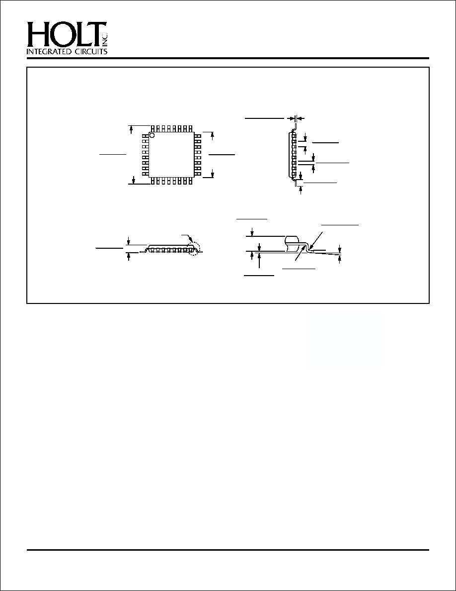
Package Type: 32PTQS
32 PIN PLASTIC THIN QUAD FLAT PACK (TQFP)
.3543 BSC
(9.00 BSC
)
SQ.
.063 MAX.
(1.60 MAX.
)
.0315 BSC
(0.80 BSC)
.0148
.0030
±
(0.375
±
)
.075
.0551
.002
±
(1.4
±
.05)
.0031 R MIN.
(0.08 R MIN.)
.0039
.002
±
(0.10
±
)
.05
0∞
7∞
.2755 BSC
(7.00 BSC)
SQ.
See Detail A
Detail A
.0055R
.0024
±
(0.14R
±
)
.06
.0236
.0059
±
(0.60
±
)
.15
.00057
.00022
±
(0.0145
±
)
.0055