 | ÐлекÑÑоннÑй компоненÑ: HX84050 | СкаÑаÑÑ:  PDF PDF  ZIP ZIP |
HX84050.pdf
A major emphasis in Honeywell's packaging program is the
use of multichip modules (MCMs). Use of multichip mod-
ules will result in higher density packaging of integrated
circuits (ICs) and components, lower weight and volume
associated with size reduction, higher performance due to
a decrease in interconnect length, and additional improve-
ment with new material systems. Honeywell has had a
leading role in the development and application of space
qualified multichip modules for the last 14 years. In con-
junction with the basic technology, we have also developed
the necessary tools and methodology for the design of
MCMs, Known Good Die (KGD) testing, materials/pro-
cesses for assembly of MCMs, and test capability for MIL
STD and QML screening.
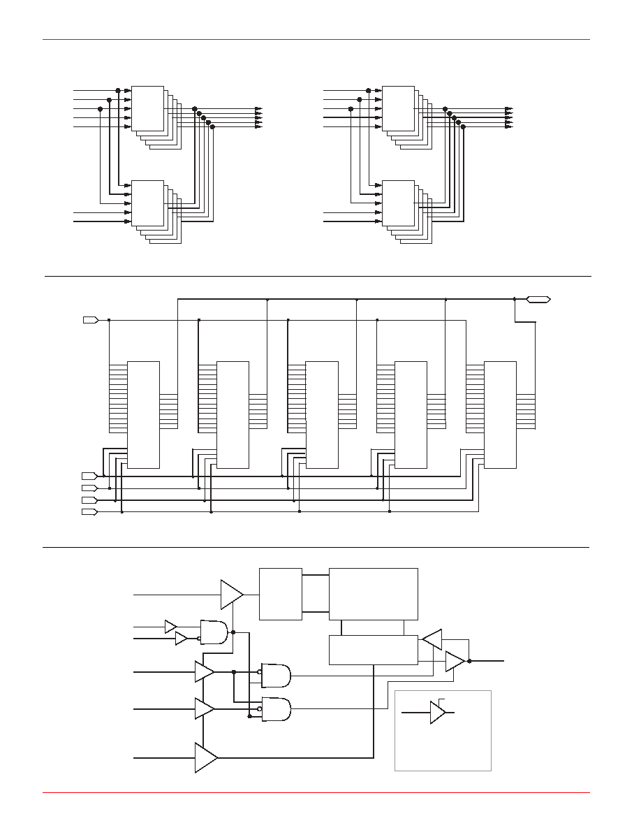
The 5M Memory Module is organized into two separate
64K x 40 memory banks. Each memory bank contains two
32K x 40 blocks, using five SRAMs each. The two banks
of memory are connected to different busses, making
Military & Space Products
5 MEGABIT MEMORY MODULE
HX84050
OTHER
· Listed on SMD #5962-96840
· Read/Write Cycle Times
20 ns (Typical)
30 ns (-55 to 125
°
C)
· Asynchronous Operation
· CMOS Compatible I/O
· Single 5 V
±
10% Power Supply
· Low Operating Power
· 200-Lead Quad Flat Pack (2.1 in. x 2.1 in.)
GENERAL DESCRIPTION
RADIATION
·
Fabricated with RICMOS
TM
IV Silicon on Insulator
(SOI) 0.75
µ
m Process (L
eff
= 0.6
µ
m)
·
Total Dose Hardness through 1x10
6
rad (SiO
2
)
·
Neutron Hardness through 1x10
14
cm
-2
·
Dynamic and Static Transient Upset Hardness
through 1x10
9
rad (Si)/s
·
Dose Rate Survivability through 1x10
11
rad(Si)/s
·
Soft Error Rate of <1x10
-10
Upsets/bit-day
in Geosynchronous Orbit
·
No Latchup
them logically and physically separate within each bank.
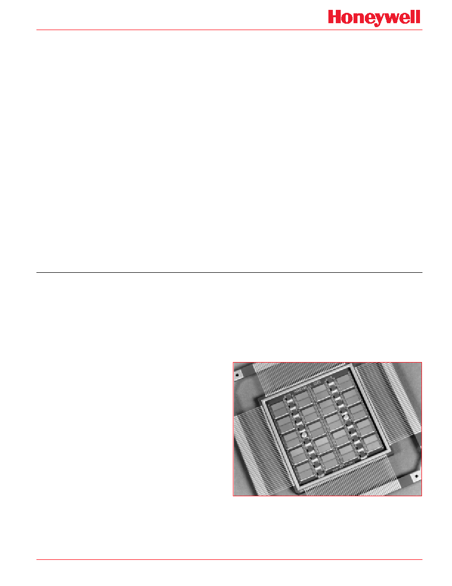
Only one block is enabled and consuming power at any
given time. The die are packaged in a 200-pin 2.1" x 2.1" co-
fired substrate ceramic flat package.
HX84050
2
NCS
A:3-7,12,14-16
CE
NWE
NOE
WE · CS · CE
NWE · CS · CE · OE
Column Decoder
Data Input/Output
Row
Decoder
32,768 x 8
Memory
Array
A:0-2, 8-11, 13
#
Signal
All controls must be
enabled for a signal to
pass. (#: number of
buffers, default = 1)
1 = enabled
Signal
8
DQ:0-7
(0 = high Z)
·
·
·
· · ·
8
8
9
Figure 2. 32K x 40 Memory Block Functional Diagram
Figure 3. 32K x 8 SRAM Functional Diagram
FUNCTIONAL DIAGRAMS
Figure 1. 2 x 64K x 40 (Top Level Diagram)
I_DATA(39:0)
32Kx8
Die
32Kx8
Die
I_Address(14:0)
I_NOE
I_NWE
I_CE0
I_NCS0
I_CE1
I_NCS1
}
64K x 40 Memory Bank I
32K x 40 Memory Block 0
32K x 40 Memory Block 1
D_DATA(39:0)
32Kx8
Die
32Kx8
Die
D_Address(14:0)
D_NOE
D_NWE
D_CE0
D_NCS0
D_CE1
D_NCS1
}
32K x 40 Memory Block 0
32K x 40 Memory Block 1
64K x 40 Memory Bank D
A14
A13
A12
A11
A10
A9
A8
A7
A6
A5
A4
A3
A2
A1
A0
DQ7
DQ6
DQ5
DQ4
DQ3
DQ2
DQ1
DQ0
CE
NCS
NWE
NOE
U1
32Kx8 Memory
A14
A13
A12
A11
A10
A9
A8
A7
A6
A5
A4
A3
A2
A1
A0
U2
32Kx8 Memory
A14
A13
A12
A11
A10
A9
A8
A7
A6
A5
A4
A3
A2
A1
A0
U3
32Kx8 Memory
A14
A13
A12
A11
A10
A9
A8
A7
A6
A5
A4
A3
A2
A1
A0
U4
32Kx8 Memory
A14
A13
A12
A11
A10
A9
A8
A7
A6
A5
A4
A3
A2
A1
A0
U5
32Kx8 Memory
ADDRESS (14 : 0)
DATA (39 : 0)
I_CE0
I_NCS0
I_NWE
I_NOE
BANK I, BLOCK 0
DQ7
DQ6
DQ5
DQ4
DQ3
DQ2
DQ1
DQ0
DQ7
DQ6
DQ5
DQ4
DQ3
DQ2
DQ1
DQ0
DQ7
DQ6
DQ5
DQ4
DQ3
DQ2
DQ1
DQ0
DQ7
DQ6
DQ5
DQ4
DQ3
DQ2
DQ1
DQ0
CE
NCS
NWE
NOE
CE
NCS
NWE
NOE
CE
NCS
NWE
NOE
CE
NCS
NWE
NOE
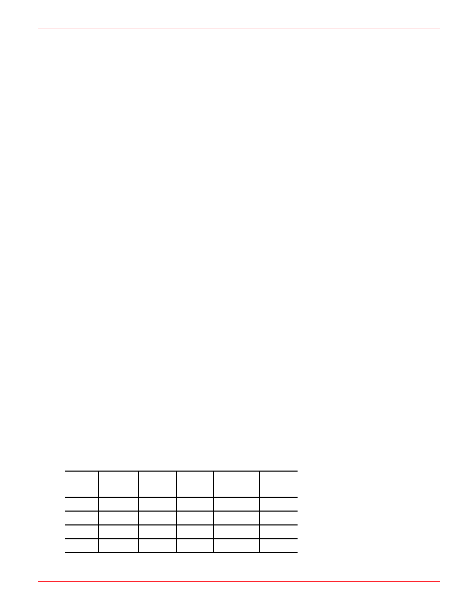
HX84050
3
CE
NCS
NWE
NOE
MODE
DQ
H
L
H
L
Read
Data Out
H
L
L
X
Write
Data In
X
H
XX
XX
Deselected
High Z
L
X
XX
XX
Disabled
High Z
TRUTH TABLE
Notes:
X: VI=VIH or VIL
XX: VSS
VI
VDD
NOE=H: High Z output state maintained
for NCS=X, CE=X, NWE=X
SIGNAL DEFINITIONS
Signal definitions for an individual SRAM within the five chip 32K x 40 memory block are shown below.
A: 0 - 14
Address input pins (A) which select a particular eight bit word within the memory array.
A: 0-3 (Column Select)
A: 4-11 (Row Select)
A: 12-14 (Block Select)
DQ: 0 - 7
Bi-directional data pins which serve as data outputs during a read operation and as data inputs during a write
operation.
NCS
Negative chip select, when at a low level, allows normal read or write operation. When at a high level it
defaults the SRAM to a pre-charge condition and holds the data output drivers in a high impedance state.
All input signals except NCS and CE are disabled. The dynamic and DC IDD chip current contribution from
all other input circuits caused by input pins transitioning and/or at VDD or VSS is eliminated. If the NCS signal
is not used it must be connected to VSS.
NWE
Negative write enable, when at a low level activates a write operation and holds the data output drivers in
a high impedance state. When at a high level it allows normal read operation.
NOE
Negative output enable, when at a high level holds the data output drivers in a high impedance state. When
at a low level, the data output driver state is defined by NCS, NWE and CE. If the NOE signal is not used
it must be connected to VSS.
CE
Chip enable, when at a high level, allows normal operation. When at a low level it forces the array to a pre-
charge condition, holds the data output drivers in a high impedance state and disables all the input buffers
except CE and NCS. The dynamic and DC IDD chip current contribution from all other input circuits caused
by input pins transitioning and/or not at VDD or VSS levels is eliminated. If the CE signal is not used it must
be connected to VDD.
HX84050
4
Total Dose
1x10
6
rad(SiO
2
)
Transient Dose Rate Upset
1x10
9
rad(Si)/s
Transient Dose Rate Survivability
1x10
11
rad(Si)/s
Soft Error Rate
<1x10
-10
upsets/bit-day
Neutron Fluence
1x10
14
N/cm
2
Parameter
Limits (2)
Test Conditions
RADIATION HARDNESS RATINGS (1)
Total Ionizing Radiation Dose
The memory module will meet all stated functional and
electrical specifications over the entire operating tempera-
ture range after the specified total ionizing radiation dose.
All electrical and timing performance parameters will re-
main within specifications after rebound at VDD = 5.5 V
and T =125
°
C extrapolated to ten years of operation. Total
dose hardness is assured by wafer level testing of process
monitor transistors and RAM product using 10 KeV X-ray
and Co60 radiation sources. Transistor gate threshold shift
correlations have been made between 10 KeV X-rays
applied at a dose rate of 1x10
5
rad(SiO
2
)/min at T = 25
°
C
and gamma rays (Cobalt 60 source) to ensure that wafer
level X-ray testing is consistent with standard military
radiation test environments.
Transient Pulse Ionizing Radiation
The memory module is capable of writing, reading, and
retaining stored data during and after exposure to a tran-
sient ionizing radiation pulse, up to the transient dose rate
upset specification, when applied under recommended
operating conditions.
The memory module will meet any functional or electrical
specification after exposure to the transient dose rate
survivability specification, when applied under recom-
mended operating conditions. Note that the current con-
ducted during the pulse by the RAM inputs, outputs, and
power supply may significantly exceed the normal operat-
ing levels. The application design must accommodate
these effects.
Neutron Radiation
The memory module will meet any functional or timing
specification after exposure to the specified neutron flu-
ence under recommended operating or storage conditions.
This assumes an equivalent neutron energy of 1 MeV.
Soft Error Rate
The memory module is immune to Single Event Upsets
(SEU) to the specified Soft Error Rate (SER), under recom-
mended operating conditions. This hardness level is de-
fined by the Adams 90% worst case cosmic ray environ-
ment for geosynchronous orbits.
Latchup
The memory module will not latch up due to any of the above
radiation exposure conditions when applied under recom-
mended operating conditions. Fabrication with the SIMOX
substrate material provides oxide isolation between adja-
cent PMOS and NMOS transistors and eliminates any
potential SCR latchup structures. Sufficient transistor body
tie connections to the p- and n-channel substrates are made
to ensure no source/drain snapback occurs.
Units
(1) Device will not latch up due to any of the specified radiation exposure conditions.
(2) Operating conditions (unless otherwise specified): VDD=4.5 V to 5.5 V, TA=-55
°
C to 125
°
C.
Adams 90% worst case
environment, VDD=4.5V
Pulse width
50 ns, X-ray,
VDD=6.0 V, T
A
=25
°
C
Pulse width
1
µ
s
T
A
=25
°
C, VDD=5.5V.
X-ray or Co60
1 MeV equivalent energy,
Unbiased, T
A
=25
°
C
RADIATION CHARACTERISTICS
HX84050
5
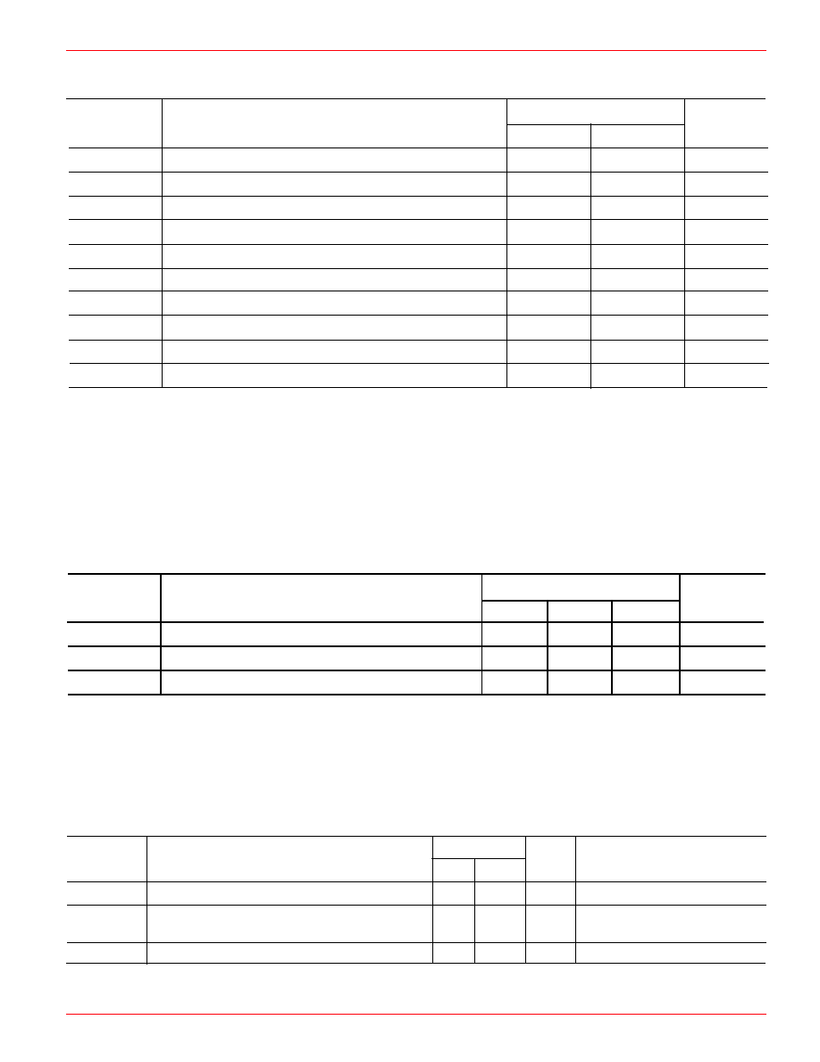
CAPACITANCE (1)
CIN1
Input Capacitance for CE and NCS Inputs
50
pF
VIN=VDD or VSS, f=1 MHz
CIN2
Input Capacitance for Address
70
pF
VIN=VDD or VSS, f=1 MHz
NOE and NWE Inputs
COUT
Output Capacitance
26
pF
VIN=VDD or VSS, f=1 MHz
Parameter
Max
Min
Symbol
Test Conditions
Worst Case
Units
(1) This parameter is tested during initial design characterization only.
(2) Worst case operating conditions: TA= -55
°
C to +125
°
C, past total dose at 25
°
C.
ABSOLUTE MAXIMUM RATINGS (1)
VDD
Supply Voltage Range (2)
-0.5
6.5
V
VPIN
Voltage on Any Pin (2)
-0.5
VDD+0.5
V
VOZ
Output Voltage Applied to High Z State (VIN and VOUT)
-0.3
VDD+0.3
V
TSTORE
Storage Temperature (Zero Bias)
-65
150
°
C
TSOLDER
Soldering Temperature (10 sec)
+288
°
C
PD
Maximum Power Dissipation (3)
5.6
W
IOUT
DC or Average Output Current
25
mA
VPROT
ESD Input Protection Voltage
2000
V
JC
Thermal Resistance (Jct-to-Case) (4)
4.0
°
C/W
TJ
Junction Temperature
175
°
C
Parameter
Symbol
Units
Max
Min
Rating
(1) Stresses in excess of those listed above may result in permanent damage. These are stress ratings only, and operation at these levels is not
implied. Frequent or extended exposure to absolute maximum conditions may affect device reliability.
(2) All voltages are referenced to VSS (VSS = ground) unless otherwise specified.
(3) Maximum power dissipation with 20 chips utilized at 50 percent (each bank is maximally utilized, alternating between blocks).
(4) Assumes a uniform temperature on the bottom surface of the package, and a uniform power distribution over the top surface of the die and all
die at equal power level.
RECOMMENDED OPERATING CONDITIONS
Symbol
Max
Typ
Description
Parameter
Min
Units
VDD
Supply Voltage (referenced to VSS)
4.5
5.0
5.5
V
TAC
Case Operating Temperature
-55
25
125
°
C
VPIN
Voltage on Any Pin (referenced to VSS)
-0.3
VDD+0.3
V