GM6486
1
GM6486
33 OUTPUT LED DRIVER
General Description
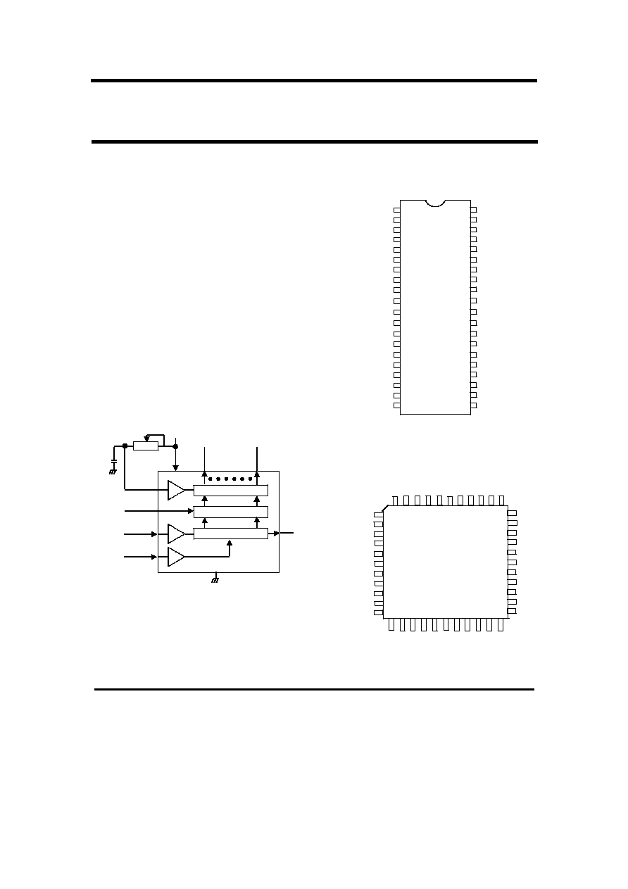
The GM6486 is a monolithic MOS integrated circuit
produced with high voltage CMOS technology. It is
available in a 40-pin dual in-line plastic package. A
sin-gle pin controls the LED display brightness by
setting a reference current through a variable
resistor connect-ed to VDD or to a separated supply
of 13.2V maximum.
Features
l
33 Output, 15mA Sink Capability
l
Current Generator Outputs (No External
Resistros Required)
l
Continous Brightness Control
l
Serial Data Input-Output
l
External Load Input
l
Cascade operation capability
l
Wide supply voltage range
l
TTL compatibility
Block Diagram
Application
l Microprocessor Displays
l Industrial control Indicator
l Relay Driver
l Instrumentation Readouts
Pin Configuration
40 PIN DIP
44 PIN PLCC
SS
V
OUT BIT 16
OUT BIT 15
OUT BIT 14
OUT BIT 13
OUT BIT 12
OUT BIT 11
OUT BIT 10
OUT BIT 9
OUT BIT 8
OUT BIT 7
OUT BIT 6
OUT BIT 5
OUT BIT 4
OUT BIT 3
OUT BIT 2
DATA OUT
BRIGHTNESS
CONTROL
OUT BIT 17
OUT BIT 18
OUT BIT 19
OUT BIT 20
OUT BIT 21
OUT BIT 22
OUT BIT 23
OUT BIT 24
OUT BIT 25
OUT BIT 26
OUT BIT 27
OUT BIT 28
OUT BIT 29
OUT BIT 30
OUT BIT 31
OUT BIT 32
OUT BIT 33
LOAD
DATA IN
CLOCK IN
DD
V
1
2
3
4
5
6
7
8
9
10
11
12
17
18
19
20
13
14
15
16
40
39
38
37
36
35
34
33
32
31
30
29
24
23
22
21
28
27
26
25
GM6486
Top View
OUT BIT 1
33 OUTPUT
BUFFES
33 LATCHES
33 BIT SHIFT REGISTER
BRIGHTNESS
CONTROL
OUTPUT BIT 33 OUTPUT BIT 1
SERIAL
DATA
LOAD
CLOCK
DATA
OUT
InF
V
DD
750
µ
100K
TYP
1 V
SS
20
24
17
18
23
22
21
OUT BIT 12
OUT BIT 11
OUT BIT 10
OUT BIT 9
OUT BIT 8
OUT BIT 7
OUT BIT 6
OUT BIT 5
OUT BIT 4
OUT BIT 3
OUT BIT 2
OUT BIT 21
OUT BIT 22
OUT BIT 23
OUT BIT 24
OUT BIT 25
OUT BIT 26
OUT BIT 27
OUT BIT 28
OUT BIT 29
OUT BIT 30
OUT BIT 31
OUT BIT 20
OUT BIT 19
OUT BIT 18
OUT BIT170
OUT BIT 16
OUT BIT 15
OUT BIT 14
OUT BIT 13
OUT BIT 20
OUT BIT 20
NC
NC
NC
NC
OUT BIT 1
LOAD
DATA OUT
BRIGHT
NES
CONTROL S
DATA IN
CLOCK IN
V
DD
V
SS
GM6486-44

GM6486
2
Absolute Maximum Rating
SYMBOL
PARAMETER
RATINGS
UNIT
DD
V
Supply Voltage
-0.3 to 15
V
IN
V
Input Voltage
-0.3 to 15
V
)
off
(
V
O
Off State Output Voltage
15
V
O
I
Output Sink Current
40
mA
1 (at 25
C
∞
)
W
tot
P
Total Package Power Dissipation
560 (at 85
C
∞
)
mW
j
T
Junction Temperature
150
C
∞
op
T
Operating Temperature Range
-25 to 85
C
∞
stg
T
Storage Temperature Range
-65 to 150
C
∞
Electrical Characteristics
(
amb
T
within operating range,
DD
V
=4.75V to 13.2V
SS
V
=0, unless otherwise specified)
SYMBOL
PARAMETER
TEST CONDITION
MIN TYP MAX UNIT
DD
V
Supply Voltage
4.75
13.2
V
DD
I
Supply Current
DD
V
=13.2V
All Control Inputs at
SS
V
=0V
50
1000
A
µ
IL
V
IH
V
Input Voltage
Logical "0" Level
Logical "1" Level
A
10
µ
±
Input Bias
25
.
5
V
75
.
4
DD
DD
V
>5.25
-0.3
2.2
DD
V
-2
0.8
DD
V
DD
V
V
V
V
b
I
Brightness input current
(Note 1)
0.75
mA
b
V
Brightness input voltage
(Pin 19)
Input Current=750
A
µ
3
4.3
V
)
off
(
V
O
Off State out. Voltage
13.2
V
OH
I
OL
I
Output sink current
(Note 2)
Segment off
Segment on
V
3
V
o
=
V
1
V
o
=
(Note 3)
Bright in =0
A
µ
Bright in =100
A
µ
Bright in =750
A
µ
0
2
12
2.7
15
10
10
4
25
A
µ
A
µ
mA
mA
O
I
Maximum Segment
Current
40
mA

GM6486
3
SYMBOL
PARAMETER
TEST CONDITION MIN TYP MAX UNIT
M
O
Output Matching
(Note 4)
20
±
%
OL
V
OH
V
Data Output
Logical "0" Level
Logical "1" Level
mA
5
.
0
I
OUT
=
A
100
I
OUT
µ
=
SS
V
2.4
0.4
DD
V
V
V
C
f
th
l
t
Clock Input
Frequency
High Time
Low Time
(notes 5 and 6)
950
950
500
KHz
ns
ns
DS
t
DH
t
Data Input
Set-up time
Hold time
300
300
ns
ns
DES
t
Data Enable Input
Set-up time
100
ns
Note: 1. With a fixed resistor on the brightness input, some variation in brightness will occur from one device
to another.
2. Absolute maximum for each output should be limited to 40 mA.
3. The
o
V
voltage should be regulated by the user. See figures 6 and 7 for allowable
o
V
versus
o
I
operation.
4. Output matching is calculated as the percent variation (lmax+lmin)/2.
5. AC input waveform specification for test prupose:
ns
20
t
r
.
ns
20
t
f
.
f=500kHz
±
10% duty cycle
6. Clock Input rise and fall times must not exceed 300ns.
Functional Description
The GM6486 is specifically designed to operate 4 digit displays with minimal interface with the display and the
data source. Serial data transfer from the data source to the display driver is accomplished with 3 signals, serial
data, clock and load.
The 33 data bits are latched by a positive pulse, thus providing non-multiplexed direct drive to the display.
Outputs change only if the serial data bits differ from the previous time. Display brightness is determined by con-
trol of the output current of LED drivers. A 1nF capacitor should be connected to brightness control, pin 19, to
prevent possible oscillation. A block diagram is shown in figure 1.
The output current is typically 20 times greater than the current into pin 19, which is set by an external variable resistor.
There is an internal limiting resistor of 400
nominal value.
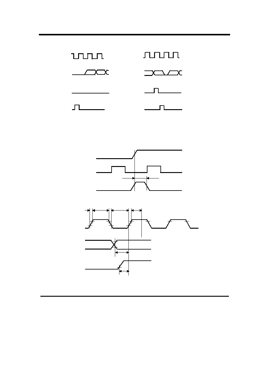
Figure 2 and 3 show the input data format. Bit "1" is the first bit into the data input pin and it will appear on pin
17. A logical "1" at the input will turn on the appropriate LED. The LOAD signal latches the 33 bit of the shift
registers into the latches. The data out pin allows for cascading the shift registers for more than 33 output drivers.
When power is first applied to the chip an internal power ON reset signal is generated which resets all registers
and all latches.
The first clock return the chip to its normal operation.
Figure 4 shows the timing relationship between data, clock and load.
A max clock frequency of 0.5MHz is assumed.
For applications where less number of outputs are used, it is possible to either increase the current per output or
operate the part at higher than 1V
o
V
.
The following equation can be used for calculation.
∑
∑
=
)
I
(
)
V
[(
T
LED
o
j
(No. of segments)+(Vdd
◊
7mA)](124 C
∞
/W)+Tamb
where
=
j
T
junction temperature (+150
C
∞
max) 124
C
∞
/W=thermal coefficient of package
o
V
=the voltage at the LED driver outputs Temb=ambient temperature
LED
I
=the LED current
The above equation was used to plot figure 5, 6 and 7.
GM6486
4
∑
leading clock is necessary after power on and load signal high.
∑
reset pulse 1: internal pulse that comes after power on--
effective on both shift register and latches
∑
reset pulse 2: internal pulse that comes load pulse--
effective on shift register only.
Fig. 2. Data Input Format
Fig. 3. Power On Reset
Fig. 4. Timing Diagram
CLOCK
LEADING
CLOCK
LEADING
CLOCK
DATA
LOAD
RESET
(INTERNAL)
BIT 1 BIT 2
BIT 32 BIT 33
BIT 1
reset
Pulse 1
reset
Pulse 2
VDD
CLOCK
RESET
(INTERNAL)
300ns MIN
CLOCK
DATA
LOAD
r
t
t
h
f
t
l
t
dh
t
ds
t
des
t
1
2
1
32
33
