The GM71C(S)17803C/CL is the new
generation dynamic RAM organized 2,097,152
x 8 bit. GM71C(S)17803C/CL has realized
higher density, higher performance and various
functions by utilizing advanced CMOS process
technology. The GM71C(S)17803C/CL offers
Extended Data out(EDO) Page Mode as a high
speed access mode. Multiplexed address inputs
p e r m i t t h e G M 7 1 C ( S ) 1 7 8 0 3 C / C L t o b e
packaged in standard 400 mil 28 pin plastic
SOJ, and standard 400mil 28pin plastic TSOP
II. The package size provides high system bit
densities and is compatible with widely
available automated testing and insertion
equipment.
Description
Features
* 2,097,152 Words x 8 Bit Organization
* Extended Data Out Mode Capability
* Single Power Supply (5V+/-10%)
* Fast Access Time & Cycle Time
* Low Power
Active : 715/660/605/550mW (MAX)
Standby : 11mW (CMOS level : MAX)
0.83mW (L-version : MAX)
* RAS Only Refresh, CAS before RAS Refresh,
Hidden Refresh Capability
* All inputs and outputs TTL Compatible
* 2048 Refresh Cycles/32ms
* 2048 Refresh Cycles/128ms (L- version)
* Battery Back Up Operation (L- version)
* Self Refresh Operation (L-version)
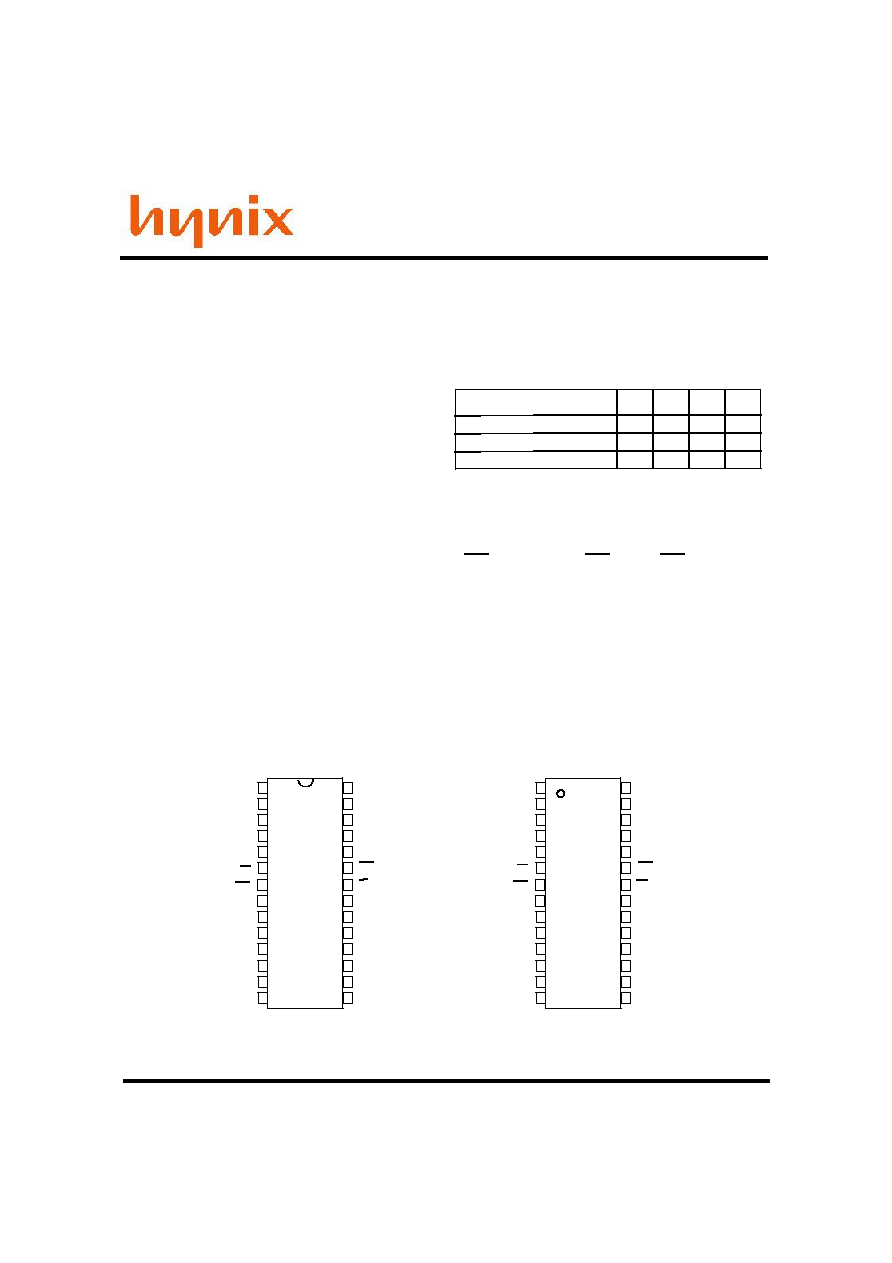
Pin Configuration
2,097,152 WORDS x 8 BIT
CMOS DYNAMIC RAM
(Top View)
28 SOJ
V
CC
I/O0
I/O1
I/O2
I/O3
1
2
3
4
5
WE
RAS
A10
A0
A1
7
8
9
10
11
6
A2
A3
V
CC
12
13
14
V
SS
I/O7
I/O6
I/O5
I/O4
24
25
26
27
28
OE
A8
A7
A6
18
19
20
21
22
CAS
23
A5
A4
V
SS
15
16
17
NC
A9
(Unit: ns)
GM71C(S)17803C/CL-5
GM71C(S)17803C/CL-6
GM71C(S)17803C/CL-7
t
RAC
t
CAC
t
RC
t
HPC
50
60
13
15
84
104
20
25
70
18
124
30
28 TSOP II
V
SS
I/O7
I/O6
I/O5
I/O4
CAS
V
SS
V
CC
I/O0
I/O1
I/O2
I/O3
1
2
3
4
5
WE
RAS
A10
A0
A1
7
8
9
10
11
6
A2
A3
V
CC
12
13
14
24
25
26
27
28
OE
NC
A8
A7
A6
18
19
20
21
22
23
A5
A4
15
16
17
A9
V
SS
I/O7
I/O6
I/O5
I/O4
CAS
V
SS
GM71C17803C
GM71CS17803CL
Rev 0.1 / Apr'01
GM71C17803C
GM71CS17803CL
Rev 0.1 / Apr'01
Pin Description
Pin
Function
Pin
Function
A0-A10
A0-A10
I/O0-I/O7
WE
V
CC
V
SS
NC
Address Inputs
Refresh Address Inputs
Data-In/Out
Row Address Strobe
Read/Write Enable
Power (+5V)
Ground
No Connection
Ordering Information
RAS
Column Address Strobe
OE
Output Enable
CAS
Absolute Maximum Ratings*
P
T
1.0
Power Dissipation
W
Symbol
Parameter
Rating
Unit
T
A
T
STG
V
IN/
V
OUT
V
CC
I
OUT
0 ~
+
70
-55 ~
+
125
50
Ambient Temperature under Bias
Storage Temperature (Plastic)
Voltage on any Pin Relative to V
SS
Supply voltage Relative to V
SS
Short Circuit Output Current
C
C
V
V
mA
-1.0 ~
+
7.0
-1.0 ~
+
7.0
Type No.
Access Time
Package
GM71C(S)17803CJ/CLJ -5
GM71C(S)17803CJ/CLJ -6
GM71C(S)17803CJ/CLJ -7
50ns
60ns
70ns
400 Mil
28 Pin
Plastic SOJ
50ns
60ns
70ns
400 Mil
28 Pin
Plastic TSOP II
GM71C(S)17803CT/CLT -5
GM71C(S)17803CT/CLT -6
GM71C(S)17803CT/CLT -7
Recommended DC Operating Conditions (T
A
= 0 ~
+
70C)
Symbol
Parameter
Unit
V
CC
V
IH
V
IL
Supply Voltage
Input High Voltage
Input Low Voltage
V
V
V
Max
5.5
6.0
0.8
Typ
5.0
-
-
Min
4.5
2.4
-1.0
Note: All voltage referred to Vss.
Note: Operation at or above Absolute Maximum Ratings can adversely affect device reliability.

GM71C17803C
GM71CS17803CL
Rev 0.1 / Apr'01
DC Electrical Characteristics (V
CC
= 5V+/-10%, Vss = 0V, T
A
= 0 ~ 70C)
Symbol
Parameter
Note
V
OH
V
OL
Output Level
Output "H" Level Voltage (I
OUT
=
-2mA
)
Unit
Max
V
CC
0.4
Min
2.0
0
Output Level
Output "L" Level Voltage (I
OUT
=
2
mA)
I
CC1
130
-
Operating Current
Average Power Supply Operating Current
(RAS, CAS Cycling
:
t
RC
=
t
RC
min)
50ns
60ns
70ns
120
110
-
I
CC2
Standby Current (TTL)
Power Supply Standby Current
(RAS, CAS = V
IH
,
D
OUT
=
High-Z)
2
-
I
CC3
RAS Only Refresh Current
Average Power Supply Current
RAS Only Refresh Mode
(t
RC
=
t
RC
min)
I
CC4
-
I
CC5
Standby Current (CMOS)
Power Supply Standby Current
(RAS, CAS
>
V
CC
- 0.2V, D
OUT
= High-Z)
1
-
I
CC6
CAS-before-RAS Refresh Current
(t
RC
=
t
RC
min)
130
-
50ns
60ns
70ns
-
-
I
CC7
150
-
I
L(I)
10
-10
I
L(O)
10
-10
Input Leakage Current
Any Input (0V
<=
V
IN
<=
6V)
Output Leakage Current
(D
OUT
is Disabled, 0V
<=
V
OUT
<=
6V)
Note: 1. I
CC
depends on output load condition when the device is selected.
I
CC
(max) is specified at the output open condition.
2. Address can be changed once or less while RAS = V
IL
.
3. Address can be changed once or less while CAS = V
IH
.
4. CAS = L (
<=
0.2V) while RAS = L (
<=
0.2V).
5. L-version.
EDO Page Mode Current
Average Power Supply Current
EDO Page Mode
(t
HPC
= t
HPC
min)
120
110
130
-
50ns
60ns
70ns
120
110
-
-
-
130
-
50ns
60ns
70ns
120
110
-
I
CC8
V
V
mA
1, 2
mA
mA
2
mA
1, 3
mA
mA
uA
uA
-
5
Standby Current RAS = V
IH
CAS = V
IL
D
OUT
=
Enable
1
mA
uA
5
Battery Back Up Operating Current(Standby with CBR Refresh)
(CBR refresh, t
RC
=62.5us
,
t
RAS
<=
0.3
us,
D
OUT
=
High-Z ,CMOS interface)
500
-
4,5
uA
I
CC9
uA
Self-Refresh Mode Current
(RAS, CAS<=0.2V
,
D
OUT
=
High-Z)
300
-
5

GM71C17803C
GM71CS17803CL
Rev 0.1 / Apr'01
Capacitance (V
CC
= 5V+/-10%, T
A
= 25C)
Symbol
Parameter
Note
C
I1
C
I2
C
I/O
Input Capacitance (Address)
Input Capacitance (Clocks)
Output Capacitance (Data-In/Out)
1
1
1, 2
Unit
pF
Max
5
7
7
Min
-
-
-
Note: 1. Capacitance measured with Boonton Meter or effective capacitance measuring method.
2. CAS = V
IH
to disable D
OUT
.
AC Characteristics (V
CC
= 5V+/-10%, T
A
= 0 ~
+
70C, Vss = 0V Note 1, 2, 18)
Test Conditions
Input rise and fall times : 2 ns
Output timing reference levels : 0.8V, 2.0V
Input timing reference levels : 0.8V, 2.4V Output load : 1TTL gate + C
L
(100 pF)
(Including scope and jig)
pF
pF
Read, Write, Read-Modify-Write and Refresh Cycles (Common Parameters)
Symbol
Parameter
Note
Max
Unit
Min
Max
Min
Max
Min
t
RC
Random Read or Write Cycle Time
84
-
104
-
124
-
t
RP
RAS Precharge Time
30
-
40
-
50
-
t
RAS
RAS Pulse Width
50
10,000
60
10,000
70
10,000
t
CAS
CAS Pulse Width
7
10,000
10,000
10,000
10
13
t
ASR
Row Address Set up Time
0
-
-
-
0
0
t
RAH
Row Address Hold Time
7
-
-
-
10
10
t
ASC
Column Address Set-up Time
0
-
-
-
0
0
t
CAH
Column Address Hold Time
7
-
-
-
10
13
t
RCD
RAS to CAS Delay Time
11
37
45
52
14
14
3
t
RAD
RAS to Column Address Delay Time
9
25
30
35
12
12
4
t
RSH
RAS Hold Time
10
-
-
-
13
13
t
CSH
CAS Hold Time
35
-
-
-
40
45
t
CRP
CAS to RAS Precharge Time
5
-
-
-
5
5
t
T
Transition Time (Rise and Fall)
2
50
50
50
2
2
7
t
DZO
OE Delay Time from D
IN
0
-
-
-
0
0
t
DZC
CAS Delay Time from D
IN
0
-
-
-
0
0
GM71C(S)17803
C/CL-5
OE to D
IN
Delay Time
13
-
-
-
15
18
5
6
6
t
CP
CAS Precharge Time
7
-
10
-
13
-
t
ODD
GM71C(S)17803
C/CL-6
GM71C(S)17803
C/CL-7
ns
ns
ns
ns
ns
ns
ns
ns
ns
ns
ns
ns
ns
ns
ns
ns
ns
ns

GM71C17803C
GM71CS17803CL
Rev 0.1 / Apr'01
Read Cycle
Symbol
Parameter
Note
Max
Unit
Min
Max
Min
t
RAC
Access Time from RAS
-
60
-
70
t
CAC
Access Time from CAS
-
15
-
18
t
AA
Access Time from Address
-
30
-
35
t
RCS
Read Command Setup Time
0
-
0
-
t
RCH
Read Command Hold Time to CAS
0
-
-
0
8,9
9,10,17
9,11,17
-
15
-
18
9
12
Access Time from OE
GM71C(S)17803
C/CL-6
t
OAC
GM71C(S)17803
C/CL-7
t
RRH
Read Command Hold Time to RAS
5
-
-
5
12
t
RAL
Column Address to RAS Lead Time
30
-
-
35
t
OFF
Output Buffer Turn-off Time
15
15
13
-
-
t
CAL
Column Address to CAS Lead Time
18
-
-
23
t
CLZ
CAS to Output in Low-Z
0
-
-
0
t
OEZ
Output Buffer Turn-off Time to OE
15
15
13
-
-
t
OH
Output Data Hold Time
3
-
-
3
t
OHO
Output Data Hold Time from OE
3
-
-
3
t
CDD
CAS to D
IN
Delay Time
15
-
-
18
5
t
RCHR
t
OHR
t
OFR
t
WEZ
t
WDD
t
RDD
Read Command Hold Time from RAS
60
70
Output Data hold Time from RAS
3
3
Output Buffer turn off to RAS
Output Buffer turn off to WE
WE to D
IN
Delay Time
15
15
15
15
18
18
-
-
-
-
-
-
-
-
-
-
-
-
RAS to D
IN
Delay Time
Max
Min
-
50
-
13
-
25
0
-
0
-
-
13
GM71C(S)17803
C/CL-5
5
-
25
-
13
-
15
-
0
-
13
-
3
-
3
-
13
-
50
3
13
13
13
-
-
-
-
-
-
ns
ns
ns
ns
ns
ns
ns
ns
ns
ns
ns
ns
ns
ns
ns
ns
ns
ns
ns
ns
ns
13
15
15

GM71C17803C
GM71CS17803CL
Rev 0.1 / Apr'01
Write Cycle
Symbol
Parameter
Note
Max
Unit
Min
Max
Min
t
WCS
0
-
0
-
t
WCH
10
-
13
-
t
WP
10
-
10
-
t
RWL
10
-
13
-
t
CWL
10
-
-
13
t
DS
0
-
-
0
t
DH
10
-
-
13
15
15
Write Command Setup Time
Write Command Hold Time
Write Command Pulse Width
Write Command to RAS Lead Time
Write Command to CAS Lead Time
Data-in Setup Time
Data-in Hold Time
14
GM71C(S)17803
C/CL-6
GM71C(S)17803
C/CL-7
ns
Min
0
-
7
-
7
-
-
-
0
-
-
Max
GM71C(S)17803
C/CL-5
7
7
7
ns
ns
ns
ns
ns
ns
Read- Modify-Write Cycle
Symbol
Parameter
Note
Max
Unit
Min
Max
Min
t
RWC
136
-
161
-
t
RWD
79
-
92
-
t
CWD
34
-
40
-
t
AWD
49
-
57
-
14
14
14
t
OEH
15
-
18
-
Read-Modify-Write Cycle Time
RAS to WE Delay Time
CAS to WE Delay Time
Column Address to WE Delay Time
OE Hold Time from WE
GM71C(S)17803
C/CL-6
GM71C(S)17803
C/CL-7
ns
ns
ns
ns
ns
Min
111
-
67
-
30
-
42
-
13
-
Max
GM71C(S)17803
C/CL-5
Refresh Cycle
Symbol
Parameter
Note
Max
Unit
Min
Max
Min
t
CSR
5
-
5
-
ns
t
CHR
10
-
10
-
ns
t
RPC
5
-
5
-
ns
GM71C(S)17803
C/CL-6
GM71C(S)17803
C/CL-7
t
WRP
0
-
0
-
ns
t
WRH
10
-
10
-
ns
CAS Setup Time
(CAS-before-RAS Refresh Cycle)
CAS Hold Time
(CAS-before-RAS Refresh Cycle)
RAS Precharge to CAS Hold Time
WE Setup Time
(CAS-before-RAS Refresh Cycle)
WE Hold Time
(CAS-before-RAS Refresh Cycle)
Min
5
-
7
-
5
-
GM71C(S)17803
C/CL-5
0
-
10
-
Max

GM71C17803C
GM71CS17803CL
Rev 0.1 / Apr'01
Symbol
Parameter
Note
Max
Unit
Min
Max
Min
25
-
30
-
35
-
40
-
9,17
-
-
16
100,000
100,000
-
-
35
40
GM71C(S)17803
C/CL-6
GM71C(S)17803
C/CL-7
EDO Page Mode Cycle
19
3
3
-
-
-
-
9
10
13
5
5
35
40
ns
ns
ns
ns
ns
ns
ns
ns
Min
20
-
30
-
-
-
GM71C(S)17803
C/CL-5
3
-
-
-
-
5
30
Max
100,000
7
Access Time from CAS Precharge
RAS Hold Time from CAS Precharge
EDO Page Mode RAS Pulse Width
EDO Page Mode Cycle Time
Output data Hold Time from CAS low
Read command Hold Time
from CAS Precharge
CAS Hold Time referred OE
CAS to OE Setup Time
30
EDO Page Mode Read-Modify-Write Cycle
Symbol
Parameter
Note
Max
Unit
Min
Max
Min
68
-
79
-
ns
54
-
62
-
ns
14
EDO Page Mode Read-Modify-Write
Cycle Time
WE Delay Time from CAS Precharge
GM71C(S)17803
C/CL-6
GM71C(S)17803
C/CL-7
Refresh
Symbol
Parameter
Note
Max
Unit
Min
Max
Min
32
-
-
ms
t
HPC
t
RASP
t
ACP
t
RHCP
t
DOH
t
COL
t
COP
t
RCHP
t
HPRWC
t
CPW
t
REF
t
REF
Refresh period
Refresh period (L -Series)
128
-
128
-
ms
GM71C(S)17803
C/CL-6
GM71C(S)17803
C/CL-7
32
2048
cycles
2048
cycles
Max
Min
57
-
45
-
GM71C(S)17803
C/CL-5
Max
Min
32
-
128
-
GM71C(S)17803
C/CL-5
Self Refresh Mode ( L-version )
Symbol
Parameter
Note
Max
Unit
Min
Max
Min
GM71CS17803
CL-5
GM71CS17803
CL-5
t
RASS
100
-
100
-
�
s
t
RPS
110
-
130
-
ns
t
CHS
-50
-
-50
-
ns
RAS Pulse Width ( Self-refresh )
RAS Precharge Time ( Self-refresh )
CAS Hold Time ( Self-refresh )
Min
100
-
90
-
-50
-
Max
GM71CS17803
CL-5

GM71C17803C
GM71CS17803CL
Rev 0.1 / Apr'01
AC Measurements assume t
T
= 2
ns
.
An initial pause of 200us is required after power up followed by a minimum of eight
initialization cycles (any combination of cycles containing RAS only refresh or CAS-before-
RAS refresh). If the internal refresh counter is used, a minimum of eight CAS-before-RAS
refresh cycles are required.
Operation with the t
RCD
(max) limit insures that t
RAC
(max) can be met, t
RCD
(max) is specified as a
reference point only; if t
RCD
is greater than the specified t
RCD
(max) limit, then access time is
controlled exclusively by t
CAC
.
Operation with the t
RAD
(max) limit insures that t
RAC
(max) can be met, t
RAD
(max) is specified as a
reference point only; if t
RAD
is greater than the specified t
RAD
(max) limit, then access time is
controlled exclusively by t
AA
.
Either t
ODD
or t
CDD
must be satisfied.
Either t
DZO
or t
DZC
must be satisfied.
V
IH
(min) and V
IL
(max) are reference levels for measuring timing of input signals. Also,
transition times are measured between V
IH
(min) and V
IL
(max).
Assumes that t
RCD
<= t
RCD
(max) and t
RAD
<= t
RAD
(max). If t
RCD
or t
RAD
is greater than the
maximum recommended value shown in this table, t
RAC
exceeds the value shown.
Measured with a load circuit equivalent to 1TTL loads and 100pF.
Assumes that t
RCD
>= t
RCD
(max) and t
RAD
<= t
RAD
(max).
Assumes that t
RCD
<= t
RCD
(max) and t
RAD
>= t
RAD
(max).
Either t
RCH
or t
RRH
must be satisfied for a read cycles.
t
OFF
(max) and t
OEZ
(max) define the time at which the outputs achieve the open circuit condition
and are not referred to output voltage levels.
t
WCS
, t
RWD
, t
CWD
, t
AWD
and t
CPW
are not restrictive operating parameters. They are included in the
data sheet as electrical characteristics only; if t
WCS
>=t
WCS
(min), the cycle is an early write cycle
and the data out pin will remain open circuit (high impedance) throughout the entire cycle; if
t
RWD
>=t
RWD
(min), t
CWD
>=t
CWD
(min) and t
AWD
>=t
AWD
(min), or t
CWD
>=t
CWD
(min), t
AWD
>=t
AWD
(min)
and t
CPW
>=t
CPW
(min), the cycle is a read modify write and the data output will contain data read
from the selected cell; if neither of the above sets of conditions is satisfied, the condition of the
data out (at access time) is indeterminate.
These parameters are referred to CAS leading edge in early write cycle and to WE leading edge
in a delayed write or a read modify write cycle.
t
RASP
defines RAS pulse width in EDO page mode cycles.
Access time is determined by the longest among t
AA
, t
CAC
and t
ACP
.
In delayed write or read-modify-write cycles, OE must disable output buffer prior to applying
data to the device. After RAS is reset, if t
OEH
>=t
CWL
, the I/O pin will remain open circuit (high
impedance): if t
OEH
<=t
CWL
, invalid data will be out at each I/O.
t
HPC
(min ) can be achieved during a series of EDO page mode write cycles or EDO page
mode read cycles. If both write and read operation are mixed in a EDO page mode RAS cycle
(EDO page mode mix cycle (1)(2) ),minimum value of CAS cycle
(
t
CAS
+
t
CP
+ 2
t
T
)
becomes
greater than the specified
t
HPC
(min) value.
The value of CAS cycle time of mixed EDO page
mode is shown in EDO page mode mix cycle(1) and (2).
Notes:
1.
2.
3.
4.
5.
6.
7.
8.
9.
10.
11.
12.
13.
14.
15.
16.
17.
18.
19.
GM71C17803C
GM71CS17803CL
Rev 0.1 / Apr'01
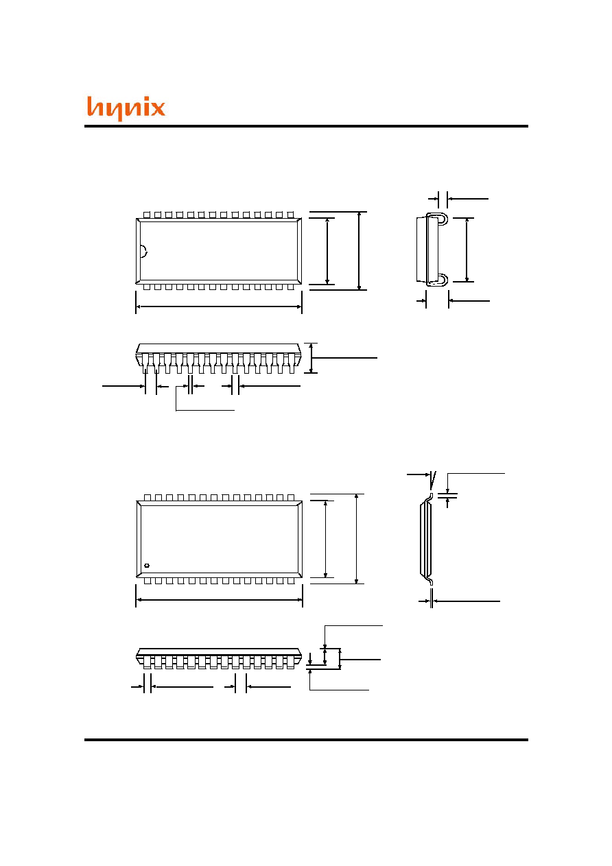
Package Dimensions
Unit: Inches (mm)
28 SOJ
28 TSOP (TYPE II)
0.405(10.29)
MAX
0.394(10.03)
MIN
0.455(11.56)
MIN
0.471(11.96)
MAX
0.730(18.54) MAX
0.720(18.28) MIN
0.020(0.50) MAX
0.012(0.30) MIN
TYP
0.050(1.27)
0.007(0.18) MAX
0.003(0.08) MIN
0.047(1.20)
MAX
0.041(1.05) MAX
0.037(0.95) MIN
0.024(0.60) MAX
0.016(0.40) MIN
0.008(0.21) MAX
0.004(0.12) MIN
0 ~ 5
o
0.395(10.03)
MIN
0.435(11.06)
MIN
0.445(11.30)
MAX
0.366(9.30)
MIN
0.375(9.55)
MAX
0.025(0.64)
MIN
0.405(10.29)
MAX
0.032(0.81) MAX
0.026(0.66) MIN
TYP
0.050(1.27)
0.020(0.50) MAX
0.015(0.38) MIN
0.148(3.75) MAX
0.128(3.25) MIN
0.710(18.04) MIN
0.720(18.30) MAX
0.083(2.10)
MIN