Äîêóìåíòàöèÿ è îïèñàíèÿ www.docs.chipfind.ru

HYNIX SEMICONDUCTOR INC.
8-BIT SINGLE-CHIP MICROCONTROLLERS
GMS81C5108
User's Manual (Ver. 1.0)

Version 1.0
Published by
MCU Application Team
©
©
©
©20
20
20
2000001111
Hynix Semiconductor Inc. All rights reserved.
Additional information of this manual may be served by Hynix Semiconductor offices in Korea or Distributors and Repre-
sentatives listed at address directory.
Hynix Semiconductor reserves the right to make changes to any information here in at any time without notice.
The information, diagrams and other data in this manual are correct and reliable; however, Hynix Semiconductor is in no
way responsible for any violations of patents or other rights of the third party generated by the use of this manual.

GMS81C5108
JUNE 2001 Ver 1.0
Table of Contents
1. OVERVIEW ...........................................1
Description .........................................................1
Features .............................................................1
Development Tools ............................................2
Ordering Information
2. BLOCK DIAGRAM ................................3
3. PIN ASSIGNMENT ...............................4
4. PACKAGE DIAGRAM ...........................5
5. PIN FUNCTION .....................................6
6. PORT STRUCTURES ...........................8
7. ELECTRICAL CHARACTERISTICS ...11
Absolute Maximum Ratings .............................11
Recommended Operating Conditions ..............11
DC Electrical Characteristics ...........................12
LCD Characteristics .........................................13
A/D Converter Characteristics .........................13
AC Characteristics ...........................................14
Serial I/O Characteristics .................................15
Typical Characteristics ..................................... 16
8. MEMORY ORGANIZATION ................18
Registers ..........................................................18
Program Memory .............................................21
Data Memory ................................................... 24
Addressing Mode ............................................. 27
9. I/O PORTS ..........................................31
Registers for Port .............................................31
I/O Ports Configuration ....................................32
10. CLOCK GENERATOR ......................34
Operation Mode ...............................................36
Operation Mode Switching ...............................37
POWER SAVING OPERATION .......................39
11. BASIC INTERVAL TIMER .................43
12. Timer / Counter .................................45
8-Bit Timer/Counter Mode ................................48
16 Bit Timer/Counter Mode ..............................50
8-Bit Capture Mode ......................................... 50
16-bit Capture Mode ....................................... 53
8-Bit (16-Bit) Compare OutPut Mode .............. 53
PWM Mode ..................................................... 53
13. Watch Timer/Watch Dog Timer......... 56
Watch Timer .................................................... 56
Watch Dog Timer ............................................ 57
14. Analog To Digital Converter ..............58
15. Buzzer Output Function ....................60
16. Serial Communication Interface ........62
Data Transmit/Receive Timing........................ 63
The method of Serial I/O ................................. 64
17. INTERRUPTS ...................................65
Interrupt Sequence .......................................... 66
BRK Interrupt .................................................. 68
Multi Interrupt .................................................. 68
External Interrupt ............................................. 69
18. KEY SCAN ........................................70
19. LCD DRIVER .................................... 71
Configuration of LCD driver ............................. 71
Control of LCD Driver Circuit ........................... 72
LCD Display Memory ...................................... 73
Control Method of LCD Driver ......................... 74
20. Remocon Carrier Generator ............. 76
Remocon Signal Output Control ..................... 76
Carrier Frequency ........................................... 77
21. OSCILLATOR CIRCUIT ....................80
22. RESET ..............................................81
External Reset Input ........................................ 81
Watchdog Timer Reset ................................... 81
23. SUPPLY VOLTAGE DETECTION ....82
24. DEVEMOPMENT TOOLS .................83
OTP Programming .......................................... 83
Emulator S/W Setting ...................................... 84
A. CONTROL REGISTER LIST ................. i
B. INSTRUCTION .................................... iii
Terminology List................................................ iii
Instruction Map ..................................................iv
Instruction Set ....................................................v
C. MASK ORDER SHEET ....................... xi
GMS81C5108
JUNE 2001 Ver 1.0
1
GMS81C5108
CMOS SINGLE-CHIP 8-BIT MICROCONTROLLER
WITH LCD CONTROLLER/DRIVER AND
INFRARED REMOTE CONTROL TRANSMITTERS
1. OVERVIEW
1.1 Description
The GMS81C5108 is an advanced CMOS 8-bit microcontroller with 8K bytes of ROM. The device is one of GMS800 fam-
ily. The Hynix GMS81C5108 is a powerful microcontroller which provides a high flexibility and cost effective solution to
many LCD applications. The GMS81C5108 provides the following standard features: 8K bytes of ROM, 192 bytes of RAM,
37 Nibbles of Display RAM, 8/16-bit timer/counter, on-chip oscillator and clock circuitry. In addition, the GMS81C5108
supports power saving modes to reduce power consumption.
This document is only explained for the base of GMS81C5108, the eliminated functions are same as below.
1.2 Features
· 8K Bytes of On-chip Program Memory
· 192 Bytes of On-chip Data RAM
· 37 Nibbles of Display RAM
· Instruction Cycle Time:
- 1us at 4MHz (2 cycle NOP instruction)
· 24 Programmable I/O pins
· 2V to 4V Operating Range
· Dual Clock Operation
- main : 400kHz ~ 4.2MHz
- sub. : 32.768kHz
· One 8-bit Basic Interval Timer/Counter
· Key Scan Interrupt
· Two 8-bit Timer/ Counter
(It can be used one 16-bit Timer/Counter)
· Watch Timer (2Hz, 4Hz, 16Hz, 1/64Hz)
· 8-bit Serial I/O (SIO)
· One 10-bit High Speed PWM Output
· Carrier Generator for Remote Controller
· 11 Interrupt sources
- 3 External interrupts (INT0 ~ 2)
- 8 Internal interrupts (BIT, Timer
×
2, WT,
A/DC, SIO, REM, Keyscan)
· 6-bit Buzzer Driving port
- 500Hz ~ 250kHz (@4MHz)
· 4-channel 8-bit On-chip A/D Converter
· Power Saving Mode
- STOP, SLEEP, Sub Active mode
· LCD display/controller (LCDC)
- Static Mode (37Seg
×
1Com, 1/3 Bias)
- 1/2 Duty Mode (36Seg
×
2Com, 1/3 Bias)
- 1/3 Duty Mode (35Seg
×
3Com, 1/3 Bias)
- 1/4 Duty Mode (34Seg
×
4Com, 1/3 Bias)
· LCD Display Voltage Booster
· Supply Voltage Detector(SVD)
- 2 level detector (2.2V, 1.7V)
Device name
ROM Size
OTP Size
RAM Size
I/O
Package
GMS81C5108
8K bytes
-
192 bytes
24
80QFP
GMS87C5108
8K bytes
192bytes
24
80QFP
GMS81C5108
2
JUNE 2001 Ver 1.0
1.3 Development Tools
Note: There are several setting switches in the Emulator.
User should read carefully and do setting properly before
developing the program refer to "24.2 Emulator S/W Set-
ting" on page 84. Otherwise, the Emulator may not work
properly.
The GMS81C5108 is supported by a full-featured macro assem-
bler, an in-circuit emulator CHOICE-Dr.
TM
and OTP program-
mers. There are two different type programmers such as single
type and gang type. For mode detail, refer to OTP Programming
chapter. Macro assembler operates under the MS-Windows 95/
98
TM
.
Please contact sales part of Hynix Semiconductor.
1.4 Ordering Information
Software
- MS- Window base assembler
- Linker / Editor / Debugger
Hardware
(Emulator)
- CHOICE-Dr.
- CHOICE-Dr. EVA 81C51 B/D
OTP Writer
- CHOICE - SIGMA (Single writer)
- CHOICE - GANG4 (Gang writer)
Device name
ROM Size (bytes)
RAM size
Package
Mask ROM version
GMS81C5108
8K bytes
192 bytes
80QFP
OTP ROM version
GMS87C5108
8K bytes OTP
192 bytes
80QFP
GMS81C5108
JUNE 2001 Ver 1.0
3
2. BLOCK DIAGRAM
ALU
LCD Controller/Driver (LCDC)
Accumulator
Stack Pointer
Interrupt Controller
Data
Memory
LCD
Memory
Display
Program
Memory
Data Table
PC
8-bit B asic
Interval Tim er
High Speed
PC
R1
R0
R3
Buzzer
Driver
PSW
System controller
Timing generator
System
Clock Controller
Clock
Generator
High freq.
Low freq.
RESET
X
IN
X
OUT
SX
IN
SX
OUT
Segment Drive Output
SEG0 ~ SEG33
Common Drive Output
COM0
R00 / INT0
R01 / INT1
R02 / INT2
R03 / EC0
R04 / BUZ
R05 / SCK
R06 / SO
R07 / SI
R10 / KS0
R11 / KS1
R12 / KS2
R13 / KS3
R14 / KS4
R15 / KS5
R16 / KS6
R17 / KS7
R30
V
DD
V
SS
Power
Supply
VCL0
VCL1
VCL2
COM1/SEG36
COM2/SEG35
COM3/SEG34
LCD Display
Voltage Booster
CAPH
CAPL
VLCDC
AV
DD
AV
SS
Power
Supply
Circuit
VREG
R20 / AN0
R31 / PWM
R32
R33
R21 / AN1
R22 / AN2
R23 / AN3
8-bit A /D
C onverter
R2
PWM
8/16-bit
T im er/C ounter
SIO
Watch/Watch Dog
Timer
WDTOUT
Remocon
(REM)
REMOUT
GMS81C5108
4
JUNE 2001 Ver 1.0
3. PIN ASSIGNMENT
AV
SS
R23 / AN3
R22 / AN2
R21 / AN1
R20 / AN0
AV
DD
SEG0
VSS
SEG1
SEG2
SEG3
SEG4
SEG5
SEG6
SEG7
SEG8
RESET
VREG
WDTOUT
SX
IN
SX
OUT
VCL0
VLCDC
VCL1
VCL2
CAPH
CAPL
COM0
SEG36 / COM1
SEG35 / COM2
SEG34 / COM3
SEG33
SE
G3
2
SE
G3
1
SE
G3
0
SE
G2
9
SE
G2
8
SE
G2
7
SE
G2
6
SE
G2
5
SE
G2
4
SE
G2
3
SE
G2
2
SE
G2
1
SE
G2
0
SE
G1
9
SE
G1
8
SE
G1
7
SE
G1
6
SE
G1
5
SE
G1
4
SE
G1
3
SE
G1
2
SE
G1
1
SE
G1
0
SE
G9
X
OUT
X
IN
V
DD
RE
MOUT
R07 /
SI
R06 /
S0
R05 /
SCK
R04 /
BUZ
R03 /
EC0
R02 /
I
N
T2
R01 /
I
N
T1
R33
R32
R31 /
PW
M
R30
R17 /
KS
7
R16 /
KS
6
R15 /
KS
5
R14 /
KS
4
R13 /
KS
3
R12 /
KS
2
R11 /
KS
1
R10 /
KS
0
R00 /
I
N
T0
1
2
3
4
5
6
7
8
9
10
11
12
13
14
15
16
17
18
19
20
21
22
23
24
64
63
62
61
60
59
58
57
56
55
54
53
52
51
50
49
48
47
46
45
44
43
42
41
40
39
38
37
36
35
34
33
32
31
30
29
28
27
26
25
65
66
67
68
69
70
71
72
73
74
75
76
77
78
79
80
GMS81C5108
GMS81C5108
JUNE 2001 Ver 1.0
5
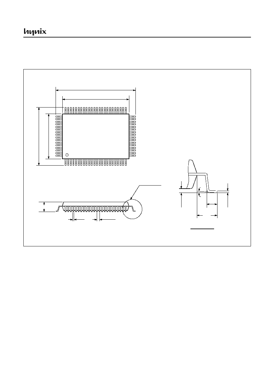
4. PACKAGE DIAGRAM
Figure 4-1 Package Diagram
20.10
19.90
24.15
23.65
18
.
1
5
17
.
6
5
14.
10
13.
90
3.10 max.
0.45
0.30
0.8 BSC
SEE DETAIL "A"
1.03
0.73
0-7
°
0.
36
0.
10
0.
23
0.
13
1.95
REF
DETAIL "A"
UNIT: mm
max
min
------------
GMS81C5108
6
JUNE 2001 Ver 1.0
5. PIN FUNCTION
V
DD
: Supply voltage.
V
SS
: Circuit ground.
AV
DD
: Supply voltage to the ladder resistor of ADC cir-
cuit. To enhance the resolution of analog to digital convert-
er, use independent power source as well as possible, other
than digital power source.
AV
SS
: ADC circuit ground
RESET: Reset the MCU.
WDTOUT: Output for detection of a program malfunc-
tion. If the user wants to use this pin, connect it to the RE-
SET pin.
REMOUT: Signal output of an infrared remote controller.
X
IN
: Input to the inverting oscillator amplifier and input to
the internal main clock operating circuit.
X
OUT
: Output from the inverting oscillator amplifier.
SX
IN
: Input to the internal sub system clock operating cir-
cuit.
SX
OUT
: Output from the inverting subsystem oscillator
amplifier.
SEG0~SEG36: Segment signal output pins for the LCD
display. See "19. LCD DRIVER" on page 71 for details.
COM0~COM3: Common signal output pins for the LCD
display. See "19. LCD DRIVER" on page 71 for details.
SEG34~SEG36 and COM1~COM3 are selected by LCDD
of the LCR register.
R00~R07: R0 is an 8-bit CMOS bidirectional I/O port. R0
pins 1 or 0 written to the Port Direction Register can be
used as outputs or inputs.
Also, pull-up resistors and open-
drain outputs can be assigned by software.
In addition, R0 serves the functions of the various follow-
ing special features.
R10~R17: R1 is an 8-bit CMOS bidirectional I/O port. R1
pins 1 or 0 written to the Port Direction Register can be
used as outputs or inputs
or schmitt trigger inputs. Also, pull-
up resistors and open-drain outputs can be assigned by software.
In addition, R1 serves the functions of the various follow-
ing special features.
R20~R23: R2 is a 4-bit CMOS bidirectional I/O port. Each
pins 1 or 0 written to the Port Direction Register can be
used as outputs or inputs.
Also, pull-up resistors and open-
drain outputs can be assigned by software.
In addition, R2 serves the functions of the various follow-
ing special features
.
R30~R33: R3 is a 4-bit CMOS bidirectional I/O port. Each
pins 1 or 0 written to the Port Direction Register can be
used as outputs or inputs.
Also, pull-up resistors and open-
drain outputs can be assigned by software.
In addition, R3 serves the functions of the various follow-
ing special features
.
VCL0~VCL2: Power supply pins for the LCD driver. The
voltage on each pin is VCL2
>
VCL1
>
VCL0. See "19.
LCD DRIVER" on page 71 for details.
VLCDC: LCD drive voltage booster reference.
CAPH, CAPL: LCD drive voltage booster capacitor.
VREG: Output of the voltage regular for the sub clock os-
cillation circuit. Connect external 0.1uF capacitor to this
pin when using the sub system clock.
Port pin
Alternate function
R00
R01
R02
R03
R04
R05
R06
R07
INT0 (External interrupt 0)
INT1 (External interrupt 1)
INT2 (External interrupt 2)
Event counter input
Buzzer Output
SCK (SPI CLK Input/Output)
SO (SPI Serial Data Output)
SI (SPI Serial Data Input)
Port pin
Alternate function
R10
R11
R12
R13
R14
R15
R16
R17
KS0 (Key scan input 0)
KS1 (Key scan input 1)
KS2 (Key scan input 2)
KS3 (Key scan input 3)
KS4 (Key scan input 4)
KS5 (Key scan input 5)
KS6 (Key scan input 6)
KS7 (Key scan input 7)
Port pin
Alternate function
R20
R21
R22
R23
AN0 (Analog Input Port0)
AN1 (Analog Input Port1)
AN2 (Analog Input Port2)
AN3 (Analog Input Port3)
Port pin
Alternate function
R31
PWM (PWM Output)
GMS81C5108
JUNE 2001 Ver 1.0
7
PIN NAME
Pin No.
Primary Function
Secondary Function
State @ Reset
State @ STOP
I/O
Description
I/O
Description
V
DD
62
-
Supply Voltage
-
-
-
-
V
SS
33
-
Circuit Ground
-
-
-
-
AV
DD
35
-
Supply Voltage for
ADC
-
-
-
-
AV
SS
40
-
Ground for ADC
-
-
-
-
RESET
65
I
Reset (low active)
-
-
`L' input
`H' input
WDTOUT
67
O
Watch dog output
-
-
Floating (To be
connect Pull-up)
State of before
STOP
REMOUT
61
O
Remocon output
-
-
`L' output
X
IN,
X
OUT
63, 64
I,O
Main clock oscillator
-
-
Oscillation
`L', `L'
SX
IN,
SX
OUT
68, 69
I,O
Sub clock oscillator
-
-
Oscillation
V
REG
66
-
Sub clock voltage
-
-
-
-
VCL0~VCL2
70,72,73
-
LCD drive voltage
-
-
Internal VCL0
Connected
State of before
STOP
VLCDC
71
-
LCD drive voltage
booster reference
-
-
-
-
CAPH,CAPL
74,75
-
LCD drive voltage
booster capacitor
-
-
Internal VCL0
Connected
State of before
STOP
SEG0 ~ SEG33 34, 32~1
O
LCD segment output
-
-
Segment output
COM0
76
O
LCD common output
-
-
Common output
SEG34/COM3
SEG35/COM2
SEG36/COM1
79~77
O
LCD common output.
-
LCD segment
output
Common output
State of before
STOP
R00/INT0
41
I/O
General I/O port
I
Interrupt Input
Input port
R01/INT1
54
I/O
I
Interrupt Input
R02/INT2
55
I/O
I
Interrupt Input
R03/EC0
56
I/O
I
Event counter input
R04/BUZ
57
I/O
O
Buzzer output
R05/SCK
58
I/O
I/O
Serial clock I/O
R06/SO
59
I/O
O
Serial Data Output
R07/SI
60
I/O
I
Serial Data Input
R10 ~ R17/
KS0 ~ KS7
42~49
I/O
I
Key wake-up input
R20 ~ R23/
AN0 ~ AN3
36~39
I/O
I
A/D converter
analog input
R30,R32,R33
50,52,53
I/O
-
-
R31/PWM
51
I/O
O
PWM output
Table 5-1 Port Function Description
GMS81C5108
8
JUNE 2001 Ver 1.0
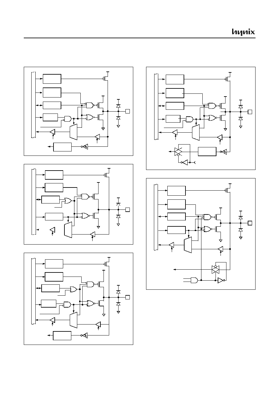
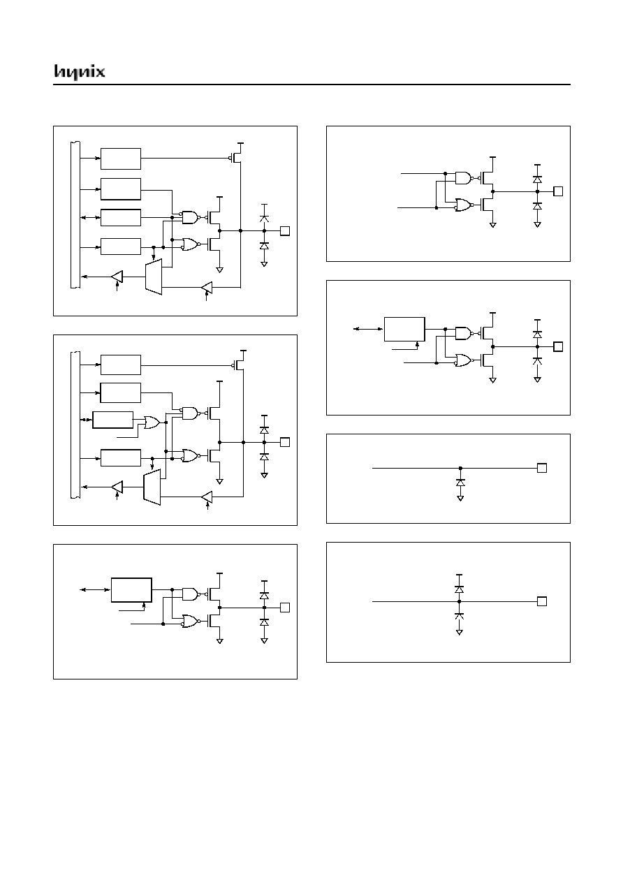
6. PORT STRUCTURES
R00~R03/INT0~INT2, R03/EC0, R07/SI
R04/BUZ, R06/SO
R05/SCK
R10~R17/KS0~KS7
R20~R23/AN0~AN3
Pin
Data Reg.
Dir. Reg.
Noise
Canceller
IN T0 ~ IN T2
P u ll up
R e g.
M U X
RD
V
DD
V
SS
Pull-up Tr.
EC0,SI
Open Drain
Reg.
RD
Da
ta
B
u
s
PMR<0:3,7>
Pin
Data Reg.
Dir. Reg.
Pull up
Reg.
M U X
RD
V
DD
V
SS
Pull-up Tr.
Open Drain
Reg.
BUZ,SO
RD
Da
t
a
Bu
s
Pin
Data Reg.
Dir. Reg.
Pull up
Reg.
M U X
RD
V
DD
V
SS
Pull-up Tr.
Open Drain
Reg.
SCK(OUT)
Noise
Canceller
SCK(IN)
RD
Da
ta
Bu
s
SCK(IN)_EN
Pin
Data Reg.
Dir. Reg.
P ull up
R eg .
M U X
RD
V
DD
V
SS
Pull-up Tr.
Open Drain
Reg.
Key Scan
Key Scan
Enable
KS0 ~ KS7
Noise
Canceller
RD
D
a
ta
B
u
s
KSMR<0:7>
Pin
Data Reg.
Dir. Reg.
P u ll up
R e g.
M U X
RD
V
DD
V
SS
Pull-up Tr.
Open Drain
Reg.
A/D converter
AN0 ~ AN3
A/D Enable
channel select
RD
Da
ta
Bu
s
GMS81C5108
JUNE 2001 Ver 1.0
9
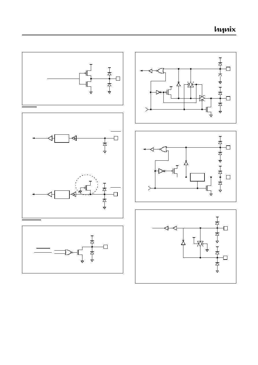
R30, R32, R33
R31
SEG0 ~ SEG33
COM0
COM1/SEG36, COM2/SEG35, COM3/SEG34
VCL0 ~ VCL2, CAPH, CAPL
VLCDC, VREG
Pin
Data Reg.
Dir. Reg.
P u ll up
R e g.
M U X
RD
V
DD
V
SS
Pull-up Tr.
Open Drain
Reg.
RD
Da
ta
Bu
s
Pin
Data Reg.
Dir. Reg.
Pull up
Reg.
M U X
RD
V
DD
V
SS
Pull-up Tr.
Open Drain
Reg.
PWMO
RD
Da
t
a
Bu
s
Pin
LCD Data
DB
VCL2 or VCL1
VCL1 or V
SS
LCD Control
Reg.
Frame Counter
VCL2
Pin
VCL2 or VCL1
VCL1 or V
SS
LCD Control
Frame Counter
VCL2
Pin
LCD Data
DB
VCL2 or VCL1
VCL1 or V
SS
LCD Control
Reg.
Frame Counter
VCL2
Pin
VCL0 ~ VCL2, CAPH, CAPL
Pin
V
DD
VCLDC, VREG
GMS81C5108
10
JUNE 2001 Ver 1.0
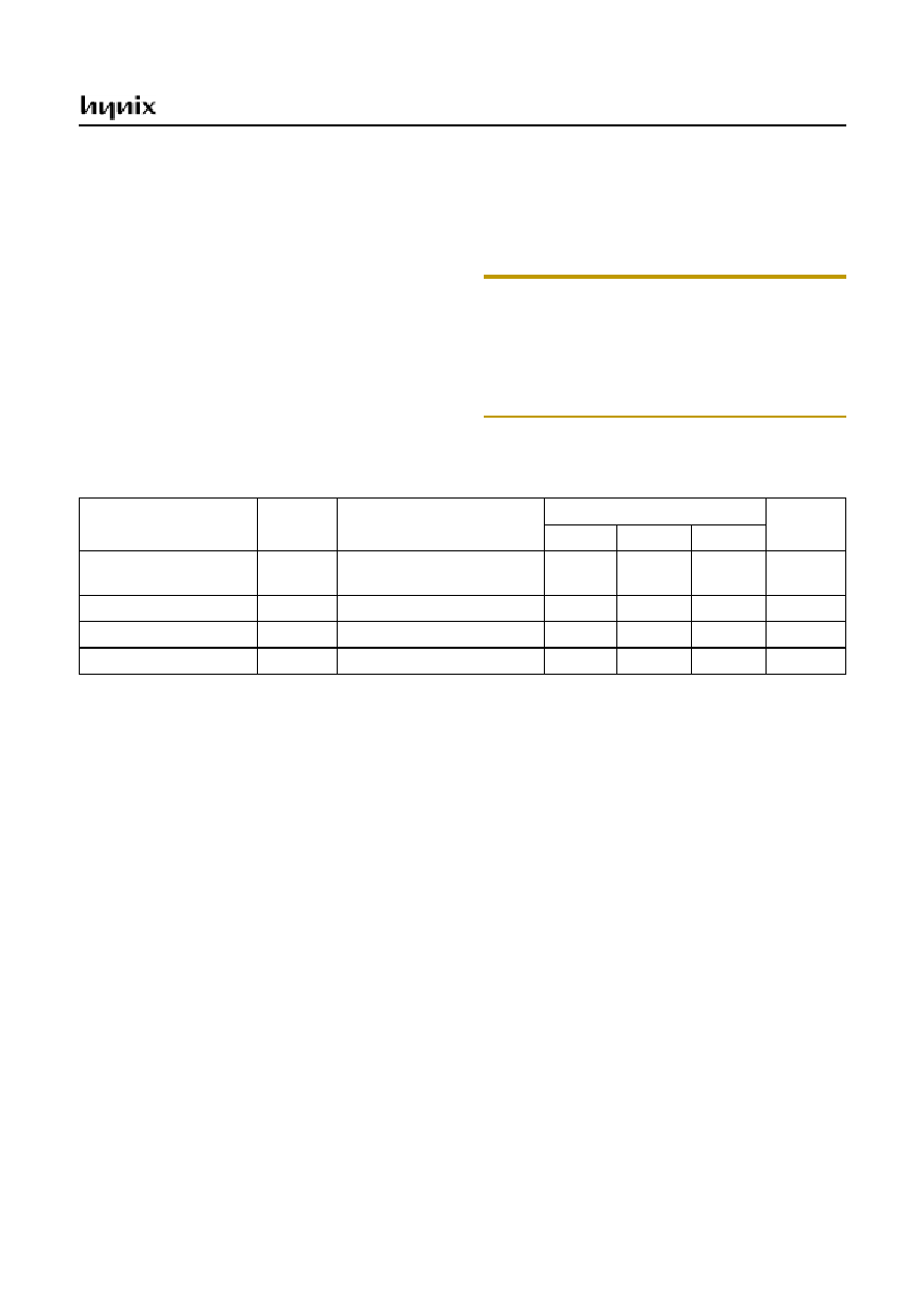
REMOUT
RESET
WDTOUT
X
IN
, X
OUT
(Crystal or Ceramic resonator Option)
X
IN
, X
OUT
(RC Option)
SX
IN
, SX
OUT
Pin
VDD
VDD
REMOUT
RESET
V
SS
Noise
Canceller
GMS87C5108 (OTP)
Internal RESET
RESET
V
DD
V
SS
Noise
Canceller
V
DD
Mask Option
Default no pull-up
Internal RESET
GMS81C5108 (MASK)
Pin
WDTOUT
WDTOUTEN
STOP
X
OUT
X
IN
V
DD
V
SS
V
DD
V
SS
V
DD
Main frequency
clock
X
OUT
X
IN
V
DD
V
SS
V
DD
V
SS
V
DD
STOP
Main frequency
clock
RC
Oscillator
Internal Cap.
= 5.0pF
SX
IN
SX
OUT
V
SS
V
DD
V
SS
V
DD
V
DD
V
SS
Sub clock
GMS81C5108
JUNE 2001 Ver 1.0
11
7. ELECTRICAL CHARACTERISTICS
7.1 Absolute Maximum Ratings
Supply voltage ........................................... -0.3 to +7.0 V
Storage Temperature ................................-40 to +125
°
C
Voltage on any pin with respect to Ground (V
SS
)
............................................................... -0.3 to V
DD
+0.3
Maximum current sunk by (I
OL
per I/O Pin) ........20 mA
Maximum output current sourced by (I
OH
per I/O Pin)
...............................................................................15 mA
Maximum current (
I
OL
) ....................................100 mA
Maximum current (
I
OH
)...................................... 60 mA
Note: Stresses above those listed under "Absolute Maxi-
mum Ratings" may cause permanent damage to the de-
vice. This is a stress rating only and functional operation of
the device at any other conditions above those indicated in
the operational sections of this specification is not implied.
Exposure to absolute maximum rating conditions for ex-
tended periods may affect device reliability.
7.2 Recommended Operating Conditions
Parameter
Symbol
Condition
Specifications
Unit
Min.
Typ.
Max.
Supply Voltage
V
DD
f
MAIN
=4MHz
f
SUB
=32.768kHz
2.0
-
4.0
V
Main Operating Frequency
f
MAIN
V
DD
=2~4V
0.4
-
4.2
MHz
Sub Operating Frequency
f
SUB
V
DD
=2~4V
-
32.768
-
kHz
Operating Temperature
T
OPR
-20
-
70
°
C
GMS81C5108
12
JUNE 2001 Ver 1.0
7.3 DC Electrical Characteristics
(TA=-20~70
°
C, V
DD
=AV
DD
=2~4V, V
SS
=AV
SS
=0V)
Parameter
Symbol
Condition
Specifications
Unit
Min.
Typ.
Max.
Input High Voltage
V
IH1
R0~R3
0.7V
DD
-
V
DD
V
V
IH2
RESET, X
IN
, INT0~INT2, EC0, SI, SCK
0.8V
DD
-
V
DD
V
IH3
SX
IN
0.8VREG
-
VREG
Input Low Voltage
V
IL1
R0~R3
0
-
0.3 V
DD
V
V
IL2
RESET, X
IN
, INT0~INT2, EC0, SI, SCK
0
-
0.2V
DD
V
IL3
SX
IN
0
-
0.2VREG
Output High Voltage
V
OH1
R0~R3, I
OH1
=-0.7mA
V
DD
-0.3
-
-
V
V
OH2
X
OUT
, I
OH2
=-50
µ
A
V
DD
-0.5
-
-
V
OH3
SX
OUT
, I
OH3
=-5
µ
A
VREG-0.3
-
-
Output Low Voltage
V
OL1
R0~R3, WDTOUT, I
OL1
=1mA
-
-
0.4
V
V
OL2
X
OUT
, I
OL2
=50
µ
A
-
-
0.5
V
OL3
SX
OUT
, I
OL3
=5
µ
A
-
-
0.5
Input High
Leakage Current
I
IH
R0~R3, V
IN
=V
DD
-
-
1
µ
A
Input Low
Leakage Current
I
IL
R0~R3, V
IN
=0V
-
-
-1
Output High
Leakage Current
I
OH
REMOUT, V
DD
=3V, V
OH
= V
DD
-1.0V
-30
-
-5
mA
Output Low
Leakage Current
I
OL
REMOUT, V
DD
=3V, V
OL
= 1.0V
0.5
-
3
Pull-up Resister
R
P1
R0~R3, V
DD
=3V
50
100
200
k
R
P2
RESET, V
DD
=3V
(GMS81C5108 Mask Option)
30
60
120
Feed Back Resister
R
F1
Main OSC Feedback Resister V
DD
=3V
0.5
-
1.5
M
R
F2
Sub OSC Feedback Resister V
DD
=3V
5.
-
15
RC Oscillator
Frequency
F
RC
R=30k
, V
DD
=3V
1
2
3
MHz
VREG Voltage
VREG
VREG=0.2uF
2.0
2.2
2.4
V
Supply Current
I
DD1
Main Active Mode
V
DD
=4V
±
10%, X
IN
=4MHz, SX
IN
=0
-
2.7
4.0
mA
I
DD2
Main Sleep Mode
V
DD
=4V
±
10%, X
IN
=4MHz, SX
IN
=0
-
0.47
1.2
I
DD3
Stop Mode
V
D D
=4V
±
10% , X
IN
=0, SX
IN
=0
-
2.0
10
µ
A
I
DD4
Sub Active mode
1
V
DD
=3V
±
10%, X
IN
=0, S
XIN
=32.768kH z
-
35(70)
80(150)
I
DD5
Sub Sleep mode
V
DD
=4V
±
10%, X
IN
=0, S
XIN
=32.768kH z
-
6.0
15
1. I
DD4 is tested by only nop operation. The value of ( ) is tested at OTP.
GMS81C5108
JUNE 2001 Ver 1.0
13
7.4 LCD Characteristics
(TA=-20~70
°
C, V
DD
=AV
DD
=2~4V, V
SS
=AV
SS
=0V)
7.5 A/D Converter Characteristics
(TA=25
°
C, V
DD
=3V, AV
DD
=3.072V, V
SS
=AV
SS
=0V)
Parameter
Symbol
Condition
Specifications
Unit
Min.
Typ.
Max.
VLCDC Output Voltage
VLCDC
V
DD
=3V, TA=25
°
C,
R1=1M
,
R2
=
300k
0.7
0.9
1.1
V
LCD Reference
Output Voltage
VCL0
External Variable Resistance
(0 to 1M
)
0.9
-
2.0
Double Output Voltage
VCL1
C1~C4=0.47uF
1.9VCL0
2.0VCL0
-
V
Triple Output Voltage
VCL2
C1~C4=0.47uF
2.85VCL0
3.0VCL0
-
LCD Common
Output Current
I
COM
Output Voltage Deviation=0.2V
30
-
-
µ
A
LCD Segment
Output Current
I
SEG
Output Voltage Deviation=0.2V
5
-
-
Parameter
Symbol
Condition
Specifications
Unit
Min.
Typ.
Max.
Analog Power Supply Input Voltage Range
AV
DD
-
AV
SS
-
AV
DD
V
Analog Input Voltage Range
V
AN
-
AV
SS
-0.3
-
AV
DD
+0.3
Current Following Between AV
DD
and AV
SS
IAV
DD
-
-
-
200
µ
A
Overall Accuracy
CAIN
-
-
±
1.0
±
2.0
LSB
Non Linearity Error
NNLE
-
-
±
1.0
±
2.0
Differential Non Linearity Error
NDNLE
-
-
±
1.0
±
2.0
Zero Offset Error
NZOE
-
-
±
0.5
±
1.5
Full Scale Error
NFSE
-
-
±
0.25
±
0.5
Gain Error
NGE
-
-
±
1.0
±
1.5
Conversion Time
TCONV
f
MAIN
=4MHz
-
-
30
µ
S
GMS81C5108
14
JUNE 2001 Ver 1.0
7.6 AC Characteristics
(TA=25
°
C, V
DD
=4V, AV
DD
=4V, V
SS
=AV
SS
=0V)
Figure 7-1 AC Timing Chart
Parameter
Symbol
Pins
Specifications
Unit
Min.
Typ.
Max.
Main Operating Frequency
f
MCP
X
IN
0.455
-
4.19
MHz
Sub Operating Frequency
f
SCP
SX
IN
30
32.768
35
kHz
System Clock Frequency
1
t
SYS
-
0.477
-
4.395
µ
S
Main Oscillation
Stabilization Time (4MHz)
t
MST
X
IN
, X
OUT
-
-
20
mS
Main Oscillation
Stabilization Time (910kHz)
-
-
60
Main Oscillation
Stabilization Time (455kHz)
-
-
100
Sub Oscillation
Stabilization Time
t
SST
SX
IN
, SX
OUT
-
1
2
S
External Clock
"H" or "L" Pulse Width
t
MCPW
X
IN
80
-
-
nS
t
SCPW
SX
IN
5
-
-
µ
S
Interrupt Pulse Width
t
IW
INT0, INT1, INT2
2
-
-
t
SYS
RESET Input Pulse "L" Width
t
RST
RESET
8
-
-
t
SYS
Event Counter Input
"H" or "L" Pulse Width
t
ECW
EC0
2
-
-
t
SYS
1.SCMR=XXXX000X that is f
MAIN
/2
X
IN
0.2V
DD
0.8V
DD
0.2V
DD
RESET
0.2V
DD
0.8V
DD
EC0
t
RST
t
ECW
t
ECW
1/f
MCP
t
MCPW
t
MCPW
SX
IN
0.2V
DD
0.8V
DD
1/f
SCP
t
SCPW
t
SCPW
t
SYS
GMS81C5108
JUNE 2001 Ver 1.0
15
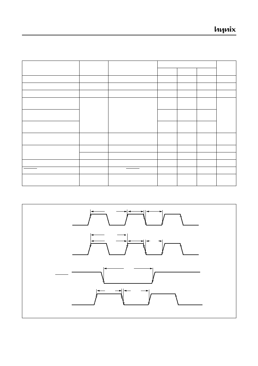
7.7 Serial I/O Characteristics
(TA=25
°
C, V
DD
=AV
DD
=2~4V, V
SS
=AV
SS
=0V)
Figure 7-2 Serial I/O Timing Chart
Parameter
Symbol
Pins
Specifications
Unit
Min.
Typ.
Max.
SCK Input Clock Pulse Period
t
SCYC
SCK
2t
SYS
+200
-
-
nS
SCK Input Clock "H" or "L" Pulse Width
t
SCKW
t
SYS
+70
-
-
SCK Output Clock Cycle Time
t
SCYC
4t
SYS
-
16t
SYS
SCK output Clock "H" or "L" Pulse Width
t
SCKW
2t
SYS
-30
-
-
SCK output Clock Delay Time
t
DS
-
-
100
SI input Setup Time (External SCK)
t
ESUS
SI
100
-
-
SI input Setup Time (Internal SCK)
t
ISUS
100
-
-
SI input Hold Time
t
HS
t
SYS
+100
-
-
SCK
t
SCKW
0.2V
DD
t
SCKW
t
SCYC
0.8V
DD
t
DS
t
SUS
t
HS
0.2V
DD
0.8V
DD
0.2V
DD
0.8V
DD
SO
SI
GMS81C5108
16
JUNE 2001 Ver 1.0
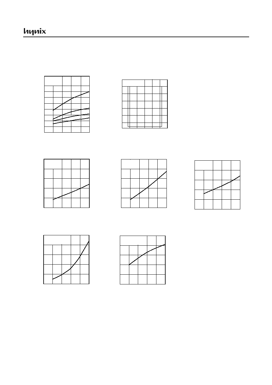
7.8 Typical Characteristics
These graphs and tables are for design guidance only and
are not tested or guaranteed.
In some graphs or tables, the datas presented are out-
side specified operating range (e.g. outside specified
V
DD
range). This is for information only and devices
are guaranteed to operate properly only within the
specified range.
The data is a statistical summary of data collected on units
from different lots over a period of time. "Typical" repre-
sents the mean of the distribution while "max" or "min"
represents (mean + 3
) and (mean
-
3
) respectively
where
is standard deviation
I
OL
-
V
OL
, V
DD
=4.2V
(mA)
I
OL
1.0
3.0
2.0
V
OL
(V)
I
OH
-
V
OH
, V
DD
=4.2V
-8
-6
-4
-2
0
(mA)
I
OH
1.0
2.0
V
OH
(V)
70
°
C
R0,R1,R2,R3 pin
R
-
-
-
-
Ta
200
100
0
(k
)
-25
0
25
75
Ta
(
°
C)
R
V
DD
=4.0V
R
-
-
-
-
Ta
100
50
0
(k
)
-25
0
25
75
Ta
(
°
C)
RESET pin
R
f
MAIN
=4MHz
V
DD
-
V
IH1
4
3
2
1
0
(V)
V
IH1
2
2.5
3
3.5
4
V
DD
(V)
Ta=25
°
C
R0~R3 pin
40
30
10
-10
-12
-14
3.0
20
f
MAIN
=4MHz
V
DD
-
V
IH2
4
3
2
1
0
(V)
V
IH2
2
2.5
3
3.5
4
V
DD
(V)
Ta=25
°
C
RESET,X
IN
,INT0~INT2,EC0.SI.SCK
-16
4.0
25
°
C
-20
°
C
4.0
-20
°
C
70
°
C
25
°
C
50
50
V
DD
=4.0V
f
MAIN
=4MHz
V
DD
-
V
IL2
2
1
0
(V)
V
IL1
2
2.5
3
3.5
4
V
DD
(V)
Ta=25
°
C
RESET,X
IN
,INT0~INT2,EC0.SI.SCK
f
MAIN
=4MHz
V
DD
-
V
IL1
2
1
0
(V)
V
IL1
2
2.5
3
3.5
4
V
DD
(V)
Ta=25
°
C
R0~R3 pin
GMS81C5108
JUNE 2001 Ver 1.0
17
I
SLEEP
(
I
DD5
)
-
V
DD
8
6
4
2
0
(
µ
A)
I
DD
2
2.5
3
3.5
4
V
DD
(V)
Sleep Mode (Sub opr.)
Ta= -20~70
°
C
(Main-clock)
Ta=25
°
C
f
MAIN
-
V
DD
4
3
2
1
0
(MHz)
f
MAIN
2
2.5
3
3.5
4
V
DD
(V)
Ta=25
°
C
R = 47k
I
DD1
-
V
DD
4
3
2
1
0
(mA)
I
DD
2
2.5
3
3.5
4
V
DD
(V)
Normal Mode (Main opr.)
6
4
2
1
0
(MHz)
f
MAIN
2
2.5
3
3.5
4.5
V
DD
(V)
Operating Area
I
STOP
(
I
DD3
)
-
V
DD
4
3
2
1
0
(
µ
A)
I
DD
2
2.5
3
3.5
4
V
DD
(V)
Stop Mode
I
DD4
-
V
DD
100
75
50
25
0
(
µ
A)
I
DD
2
2.5
3
3.5
4
V
DD
(V)
Normal Mode (Sub opr.)
I
SLEEP
(
I
DD2
)
-
V
DD
400
300
200
100
0
(
µ
A)
I
DD
2
2.5
3
3.5
4
V
DD
(V)
Sleep Mode (Main opr.)
f
MAIN
=4MHz
f
SXIN
=32kHz
Ta=25
°
C
Ta=25
°
C
f
MAIN
=0Hz
R = 68k
f
S X IN
= 3 2 kH z
Ta=25
°
C
Ta=25
°
C
f
MAIN
=4MHz
5
3
4
R = 100k
R = 20k
GMS81C5108
18
JUNE 2001 Ver 1.0
8. MEMORY ORGANIZATION
The GMS81C5108 has separate address spaces for Pro-
gram memory, Data Memory and Display memory. Pro-
gram memory can only be read, not written to. It can be up
to 8K bytes of Program memory. Data memory can be read
and written to up to 192 bytes including the stack area. Dis-
play memory has prepared 37 bytes for LCD.
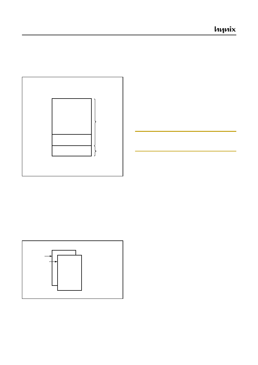
8.1 Registers
This device has six registers that are the Program Counter
(PC), a Accumulator (A), two index registers (X, Y), the
Stack Pointer (SP), and the Program Status Word (PSW).
The Program Counter consists of 16-bit register.
Figure 8-1 Configuration of Registers
Accumulator: The Accumulator is the 8-bit general pur-
pose register, used for data operation such as transfer, tem-
porary saving, and conditional judgement, etc.
The Accumulator can be used as a 16-bit register with Y
Register as shown below.
Figure 8-2 Configuration of YA 16-bit Register
X, Y Registers: In the addressing mode which uses these
index registers, the register contents are added to the spec-
ified address, which becomes the actual address. These
modes are extremely effective for referencing subroutine
tables and memory tables. The index registers also have in-
crement, decrement, comparison and data transfer func-
tions, and they can be used as simple accumulators.
Stack Pointer: The Stack Pointer is an 8-bit register used
for occurrence interrupts and calling out subroutines. Stack
Pointer identifies the location in the stack to be accessed
(save or restore).
Generally, SP is automatically updated when a subroutine
call is executed or an interrupt is accepted. However, if it
is used in excess of the stack area permitted by the data
memory allocating configuration, the user-processed data
may be lost.
The stack can be located at any position within 00
H
to BF
H
of the internal data memory. The SP is not initialized by
hardware, requiring to write the initial value (the location
with which the use of the stack starts) by using the initial-
ization routine. Normally, the initial value of "BF
H"
is
used.
Program Counter: The Program Counter is a 16-bit wide
which consists of two 8-bit registers, PCH and PCL. This
counter indicates the address of the next instruction to be
executed. In reset state, the program counter has reset rou-
tine address (PC
H
:0FF
H
, PC
L
:0FE
H
).
Program Status Word: The Program Status Word (PSW)
contains several bits that reflect the current state of the
CPU. The PSW is described in Figure 8-3. It contains the
Negative flag, the Overflow flag, the Break flag the Half
Carry (for BCD operation), the Interrupt enable flag, the
Zero flag, and the Carry flag.
[Carry flag C]
This flag stores any carry or borrow from the ALU of CPU
after an arithmetic operation and is also changed by the
Shift Instruction or Rotate Instruction.
A
ACCUMULATOR
X REGISTER
Y REGISTER
STACK POINTER
PROGRAM COUNTER
PROGRAM STATUS
WORD
X
Y
SP
PCL
PCH
PSW
Two 8-bit Registers can be used as a "YA" 16-bit Register
Y
A
Y
A
Caution:
The Stack Pointer must be initialized by software be-
cause its value is undefined after RESET.
Example: To initialize the SP
LDX
#0BFH
TXSP
; SP
BF
H
SP
0
Stack Address (00
H
~ BF
H
)
15
0
8
7
Hardware fixed
GMS81C5108
JUNE 2001 Ver 1.0
19
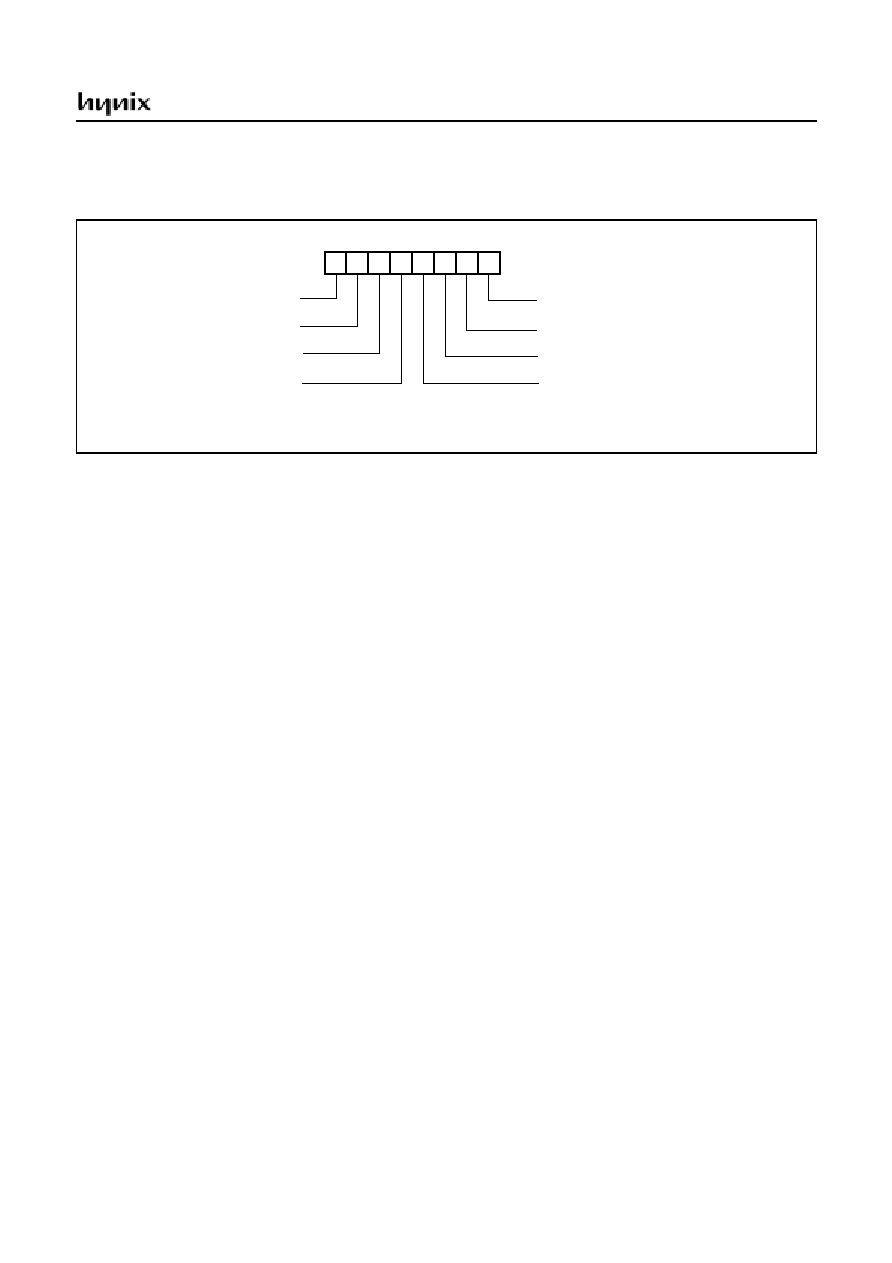
[Zero flag Z]
This flag is set when the result of an arithmetic operation
or data transfer is "0" and is cleared by any other result.
Figure 8-3 PSW (Program Status Word) Register
[Interrupt disable flag I]
This flag enables/disables all interrupts except interrupt
caused by Reset or software BRK instruction. All inter-
rupts are disabled when cleared to "0". This flag immedi-
ately becomes "0" when an interrupt is served. It is set by
the EI instruction and cleared by the DI instruction.
[Half carry flag H]
After operation, this is set when there is a carry from bit 3
of ALU or there is no borrow from bit 4 of ALU. This bit
can not be set or cleared except CLRV instruction with
Overflow flag (V).
[Break flag B]
This flag is set by software BRK instruction to distinguish
BRK from TCALL instruction with the same vector ad-
dress.
[Direct page flag G]
This flag assigns RAM page for direct addressing mode. In
the direct addressing mode, addressing area is from zero
page 00
H
to 0FF
H
when this flag is "0". If it is set to "1",
addressing area is assigned by RPR register (address
0F3
H
). It is set by SETG instruction and cleared by CLRG.
[Overflow flag V]
This flag is set to "1" when an overflow occurs as the result
of an arithmetic operation involving signs. An overflow
occurs when the result of an addition or subtraction ex-
ceeds
+
127 (7F
H
) or
-
128 (80
H
). The CLRV instruction
clears the overflow flag. There is no set instruction. When
the BIT instruction is executed, bit 6 of memory is copied
to this flag.
[Negative flag N]
This flag is set to match the sign bit (bit 7) status of the re-
sult of a data or arithmetic operation. When the BIT in-
struction is executed, bit 7 of memory is copied to this flag.
N
NEGATIVE FLAG
V
G
B
H
I
Z
C
MSB
LSB
RESET VALUE : 00
H
PSW
OVERFLOW FLAG
BRK FLAG
CARRY FLAG RECEIVES
ZERO FLAG
INTERRUPT ENABLE FLAG
CARRY OUT
HALF CARRY FLAG RECEIVES
CARRY OUT FROM BIT 1 OF
ADDITION OPERLANDS
SELECT DIRECT PAGE
when g=1, page is addressed by RPR
GMS81C5108
20
JUNE 2001 Ver 1.0
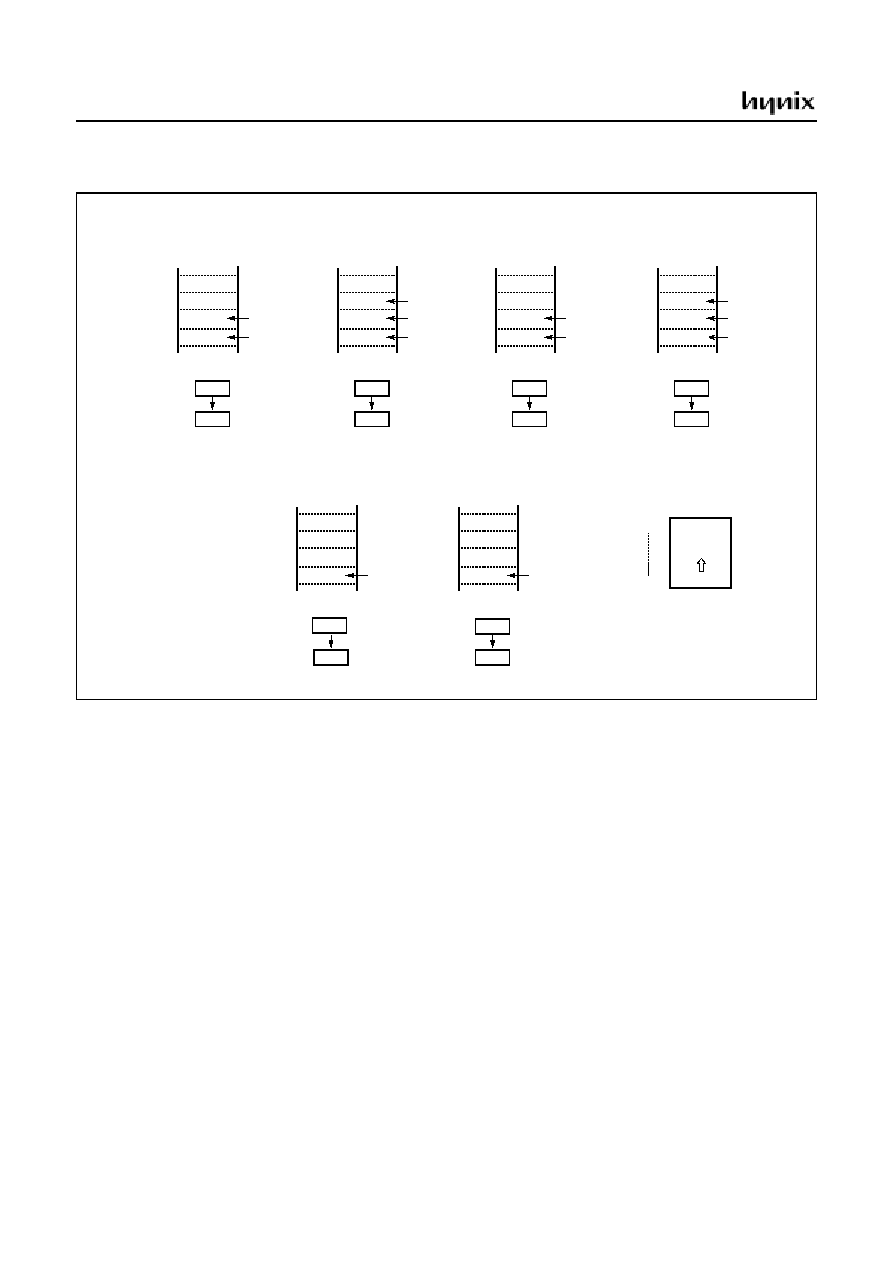
Figure 8-4 Stack Operation
At execution of a
CALL/TCALL/PCALL
PCL
PCH
00BF
SP after
execution
SP before
execution
00BD
00BE
00BD
00BC
00BF
Push
down
At acceptance
of interrupt
PCL
PCH
00BF
00BC
00BE
00BD
00BC
00BF
Push
down
PSW
At execution
of RET instruction
PCL
PCH
00BF
00BF
00BE
00BD
00BC
00BD
Pop
up
At execution
of RETI instruction
PCL
PCH
00BF
00BF
00BE
00BD
00BC
00BC
Pop
up
PSW
0000
H
00BF
H
Stack
depth
At execution
of PUSH instruction
A
00BF
00BE
00BE
00BD
00BC
00BF
Push
down
SP after
execution
SP before
execution
PUSH A (X,Y,PSW)
At execution
of POP instruction
A
00BF
00BF
00BE
00BD
00BC
00BE
Pop
up
POP A (X,Y,PSW)
GMS81C5108
JUNE 2001 Ver 1.0
21
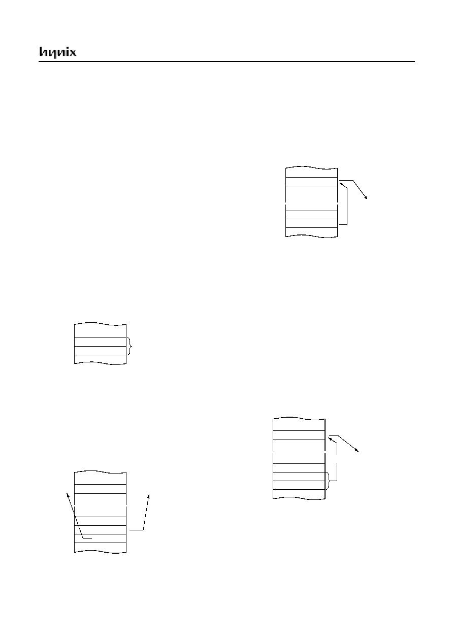
8.2 Program Memory
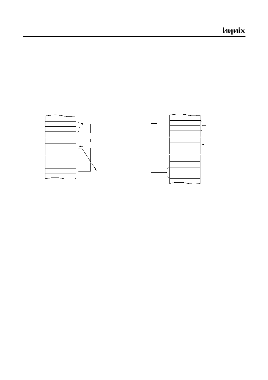
A 16-bit program counter is capable of addressing up to
64K bytes, but this device has 8K bytes program memory
space only physically implemented. Accessing a location
above FFFF
H
will cause a wrap-around to 0000
H
.
Figure 8-5 shows a map of Program Memory. After reset,
the CPU begins execution from reset vector which is stored
in address FFFE
H
and FFFF
H
as shown in Figure 8-6.
As shown in Figure 8-5, each area is assigned a fixed loca-
tion in Program Memory. Program Memory area contains
the user program.
Figure 8-5 Program Memory Map
Page Call (PCALL) area contains subroutine program to
reduce program byte length by using 2 bytes PCALL in-
stead of 3 bytes CALL instruction. If it is frequently called,
it is more useful to save program byte length.
Table Call (TCALL) causes the CPU to jump to each
TCALL address, where it commences the execution of the
service routine. The Table Call service area spaces 2-byte
for every TCALL: 0FFC0
H
for TCALL15, 0FFC2
H
for
TCALL14, etc., as shown in Figure 8-7.
Example: Usage of TCALL
The interrupt causes the CPU to jump to specific location,
where it commences the execution of the service routine.
The External interrupt 0, for example, is assigned to loca-
tion 0FFFA
H
. The interrupt service locations spaces 2-byte
interval: 0FFF8
H
and 0FFF9
H
for External Interrupt 1,
0FFFA
H
and 0FFFB
H
for External Interrupt 0, etc.
Any area from 0FF00
H
to 0FFFF
H
, if it is not going to be
used, its service location is available as general purpose
Program Memory.
Figure 8-6 Interrupt Vector Area
PROGRAM
MEMORY
TCALL
AREA
INTERRUPT
VECTOR AREA
E000
H
FEFF
H
FF00
H
FFC0
H
FFDF
H
FFE0
H
FFFF
H
PCALL
AREA
LDA
#5
TCALL 0FH
;1BYTE INSTRUCTION
:
;INSTEAD OF 2 BYTES
:
;NORMAL CALL
;
;TABLE CALL ROUTINE
;
FUNC_A:
LDA
LRG0
RET
;
FUNC_B:
LDA
LRG1
RET
;
;TABLE CALL ADD. AREA
;
ORG
0FFC0H
;TCALL ADDRESS AREA
DW
FUNC_A
DW
FUNC_B
1
2
0FFE0
H
E2
Address
Vector Area Memory
E4
E6
E8
EA
EC
EE
F0
F2
F4
F6
F8
FA
FC
FE
-
-
-
-
Serial I/O Interrupt Vector Area
AD Converter Interrupt Vector Area
Remocon Interrupt Vector Area
Timer/Counter 1 Interrupt Vector Area
Timer/Counter 0 Interrupt Vector Area
External Interrupt 1 Vector Area
Basic Interval Timer Interrupt Vector Area
Key Scan Interrupt Vector Area
RESET Vector Area
External Interrupt 0 Vector Area
External Interrupt 2 Vector Area
Watch Timer Interrupt Vector Area
"-" means reserved area.
NOTE:
GMS81C5108
22
JUNE 2001 Ver 1.0
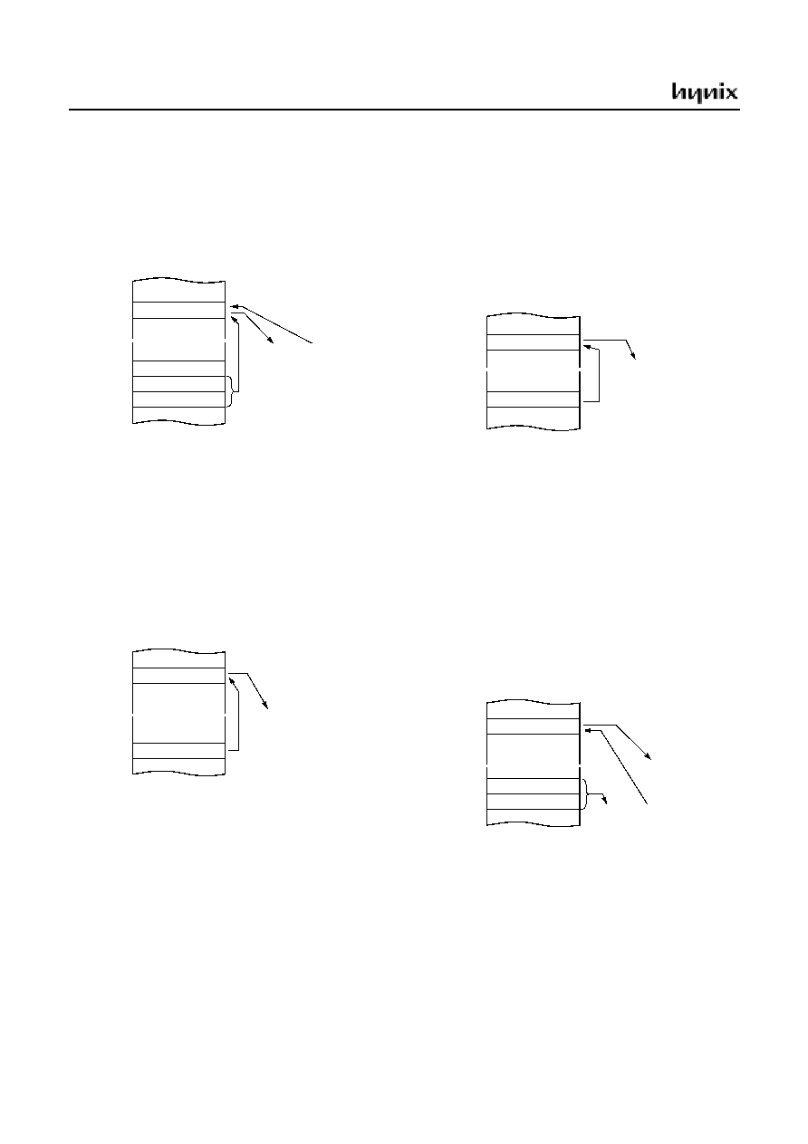
Figure 8-7 PCALL and TCALL Memory Area
PCALL
rel
4F35
PCALL
35
H
TCALL
n
4A
TCALL 4
0FFC0
H
C1
Address
Program Memory
C2
C3
C4
C5
C6
C7
C8
0FF00
H
Address
PCALL Area Memory
0FFFF
H
PCALL Area
(256 Bytes)
* means that the BRK software interrupt is using
same address with TCALL0.
NOTE:
TCALL 15
TCALL 14
TCALL 13
TCALL 12
TCALL 11
TCALL 10
TCALL 9
TCALL 8
TCALL 7
TCALL 6
TCALL 5
TCALL 4
TCALL 3
TCALL 2
TCALL 1
TCALL 0 / BRK *
C9
CA
CB
CC
CD
CE
CF
D0
D1
D2
D3
D4
D5
D6
D7
D8
D9
DA
DB
DC
DD
DE
DF
4F
~
~
~
~
NEXT
35
0FF35
H
0FF00
H
0FFFF
H
11111111 11010110
01001010
PC:
F
H
F
H
D
H
6
H
4A
~
~
~
~
25
0FFD6
H
0FF00
H
0FFFF
H
D1
NEXT
0FFD7
H
0D125
H
Reverse

GMS81C5108
JUNE 2001 Ver 1.0
23
Example: The usage software example of Vector address and the initialize part.
ORG
0FFE0H
DW
NOT_USED
DW
NOT_USED
DW
NOT_USED
DW
NOT_USED
DW
WT_INT
; Watch Timer
DW
SIO
; Serial I/O
DW
AD_Con
; AD converter
DW
Carrier_INT
; Carrier
DW
INT2
; Int.2
DW
TMR1_INT
; Timer-1
DW
TMR0_INT
; Timer-0
DW
INT1
; Int.1
DW
INT0
; Int.0
DW
BIT_INT
; BIT
DW
KEY_INT
; Key Scan
DW
RESET
; Reset
ORG
0F000H
;********************************************
;
MAIN PROGRAM *
;********************************************
;
RESET:
DI
;Disable All Interrupts
CLRG
LDX
#0
RAM_CLR:
LDA
#0
;RAM Clear(!0000
H
->!00BF
H
)
STA
{X}+
CMPX
#0C0H
BNE
RAM_CLR
;
LDX
#0BFH
;Stack Pointer Initialize
TXSP
;
CALL
LCD_CLR
;Clear LCD display memory
;
LDM
R0, #0
;Normal Port 0
LDM
R0DR,#1000_0010B
;Normal Port Direction
LDM
R0PU,#1000_0010B
;Pull Up Selection Set
LDM
R0CR,#0000_0001B
;R0 port Open Drain control
:
:
LDM
SCMR,#1111_0000B
;System clock control
:
:
GMS81C5108
24
JUNE 2001 Ver 1.0
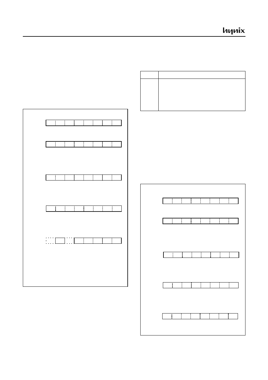
8.3 Data Memory
Figure 8-8 shows the internal Data Memory space availa-
ble. Data Memory is divided into four groups, a user RAM,
control registers, Stack, and LCD memory.
Figure 8-8 Data Memory Map
User Memory
The GMS81C5108 has 192
×
8 bits for the user memory
(RAM).
There are two page internal RAM. Page is selected by G-
flag and RAM page selection register RPR. When G-flag
is cleared to "0", always page 0 is selected regardless of
RPR value. If G-flag is set to "1", page will be selected ac-
cording to RPR value.
Figure 8-9 RAM page configuration
Control Registers
The control registers are used by the CPU and Peripheral
function blocks for controlling the desired operation of the
device. Therefore these registers contain control and status
bits for the interrupt system, the timer/ counters, analog to
digital converters and I/O ports. The control registers are in
address range of 0C0
H
to 0FF
H
.
Note that unoccupied addresses may not be implemented
on the chip. Read accesses to these addresses will in gen-
eral return random data, and write accesses will have an in-
determinate effect.
More detailed informations of each register are explained
in each peripheral section.
Note: Write only registers can not be accessed by bit ma-
nipulation instruction. Do not use read-modify-write instruc-
tion. Use byte manipulation instruction.
Example; To write at CKCTLR
LDM
CKCTLR,#05H ;Divide ratio
÷
8
Stack Area
The stack provides the area where the return address is
saved before a jump is performed during the processing
routine at the execution of a subroutine call instruction or
the acceptance of an interrupt.
When returning from the processing routine, executing the
subroutine return instruction [RET] restores the contents of
the program counter from the stack; executing the interrupt
return instruction [RETI] restores the contents of the pro-
gram counter and flags.
The save/restore locations in the stack are determined by
the stack pointed (SP). The SP is automatically decreased
after the saving, and increased before the restoring. This
means the value of the SP indicates the stack location
number for the next save. Refer to Figure 8-4 on page 20.
LCD Display Memory
LCD display data area is handled in LCD section.
See "19.3 LCD Display Memory" on page 73.
USER MEMORY
(Including STACK Area)
PERIPHERAL CONTROL
REGISTERS
MEMORY
0000
H
00BF
H
00C0
H
00FF
H
0100
H
0124
H
PAGE0
PAGE1
LCD DISPLAY
(192 Bytes)
Page 0
Page 0: 00~FF
H
Page 1
Page 1: 100~124
H
RPR=1, G=1
RPR=0, G=0
GMS81C5108
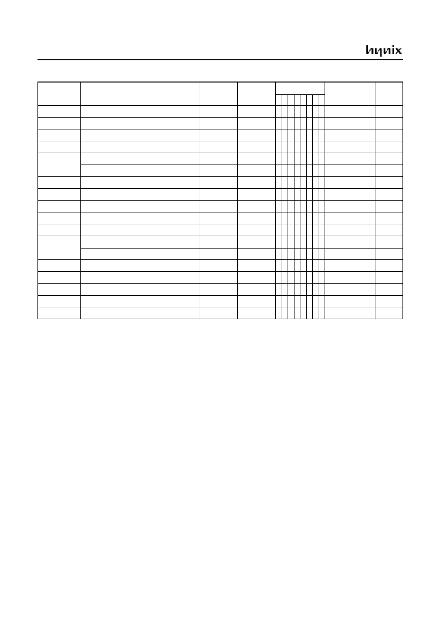
JUNE 2001 Ver 1.0
25
Address
Register Name
Symbol
R/W
Initial Value
Addressing
Mode
Page
7 6 5 4 3 2 1 0
00C0
R0 port data register
R0
R/W
0 0 0 0 0 0 0 0
byte, bit
1
32
00C1
R1 port data register
R1
R/W
0 0 0 0 0 0 0 0
byte, bit
32
00C2
R2 port data register
R2
R/W
- - - - 0 0 0 0
byte, bit
33
00C3
R3 port data register
R3
R/W
- - - - 0 0 0 0
byte, bit
33
00C8
R0 port I/O direction register
R0DR
W
0 0 0 0 0 0 0 0
byte
2
32
00C9
R1 port I/O direction register
R1DR
W
0 0 0 0 0 0 0 0
byte
32
00CA
R2 port I/O direction register
R2DR
W
- - - - 0 0 0 0
byte
33
00CB
R3 port I/O direction register
R3DR
W
- - - - 0 0 0 0
byte
33
00D0
R0 port pull-up register
R0PU
W
0 0 0 0 0 0 0 0
byte
32
00D1
R1 port pull-up register
R1PU
W
0 0 0 0 0 0 0 0
byte
32
00D2
R2 port pull-up register
R2PU
W
- - - - 0 0 0 0
byte
33
00D3
R3 port pull-up register
R3PU
W
- - - - 0 0 0 0
byte
33
00D4
R0 port open drain control register
R0CR
W
0 0 0 0 0 0 0 0
byte
32
00D5
R1 port open drain control register
R1CR
W
0 0 0 0 0 0 0 0
byte
32
00D6
R2 port open drain control register
R2CR
W
- - - - 0 0 0 0
byte
33
00D7
R3 port open drain control register
R3CR
W
- - - - 0 0 0 0
byte
33
00D8
Ext. interrupt edge selection register
IESR
R/W
- - 0 0 0 0 0 0
byte, bit
69
00D9
Port selection register
PMR
R/W
- 0 - 0 0 0 0 0
byte, bit
32
00DA
Interrupt enable low register
IENL
R/W
- 0 0 0 0 - - -
byte, bit
65
00DB
Interrupt enable high register
IENH
R/W
- 0 0 0 0 0 0 0
byte, bit
65
00DC
Interrupt request flag low register
IRQL
R/W
- 0 0 0 0 - - -
byte, bit
65
00DD
Interrupt request flag high register
IRQH
R/W
- 0 0 0 0 0 0 0
byte, bit
65
00DE
Sleep mode register
SMR
R/W
- - - - - - - 0
byte, bit
39
00E0
Timer 0 mode register
TM0
R/W
- - 0 0 0 0 0 0
byte, bit
45
00E1
Timer 0 counter register
T0
R
0 0 0 0 0 0 0 0
byte, bit
45
Timer 0 data register
TDR0
W
1 1 1 1 1 1 1 1
byte
45
Timer 0 input capture register
CDR0
R
0 0 0 0 0 0 0 0
byte, bit
45
00E2
Timer 1 mode register
TM1
R/W
0 0 0 0 0 0 0 0
byte, bit
45
00E3
Timer 1 data register
TDR1
W
1 1 1 1 1 1 1 1
byte
45
PWM0 pulse period register
T1PPR
W
1 1 1 1 1 1 1 1
byte
45
00E4
Timer 1 counter register
T1
R
0 0 0 0 0 0 0 0
byte, bit
45
Timer 1 input capture register
CDR1
R
0 0 0 0 0 0 0 0
byte, bit
45
PWM0 pulse duty register
T1PDR
R/W
0 0 0 0 0 0 0 0
byte, bit
45
00E5
PWM0 high register
PWMHR
W
- - - - 0 0 0 0
byte
45
00EC
A/D converter mode register
ADMR
R/W
- 0 - - 0 0 0 1
byte, bit
58
00ED
A/D converter data register
ADDR
R
x x x x x x x x
byte, bit
58
Table 8-1 Control Registers
GMS81C5108
26
JUNE 2001 Ver 1.0
00EF
Watch timer mode register
WTMR
R/W
- 0 0 0 0 0 0 0
byte, bit
56
00F0
Key scan mode register
KSMR
R/W
0 0 0 0 0 0 0 0
byte, bit
70
00F1
LCD control register
LCR
R/W
0 0 0 0 0 0 0 0
byte, bit
72
00F3
RAM paging register
RPR
R/W
- - - - - - 0 0
byte, bit
73
00F4
Basic interval timer register
BITR
R
0 0 0 0 0 0 0 0
byte, bit
43
Clock control register
CKCTLR
W
- - - - 0 1 1 1
byte
43
00F5
System clock mode register
SCMR
R/W
0 0 0 0 0 0 0 0
byte, bit
34
00F6
Remocon mode register
RMR
R/W
- 0 0 0 0 0 0 0
byte, bit
76
00F7
Carrier frequency high selection
CFHS
W
- - 1 1 1 1 1 1
byte
76
00F8
Carrier frequency low selection
CFLS
W
- - 1 1 1 1 1 1
byte
76
00F9
Remocon data high register
RDHR
W
1 1 1 1 1 1 1 1
byte
76
00FA
Remocon data low register
RDLR
W
1 1 1 1 1 1 1 1
byte
76
Remocon data counter
RDC
R
0 0 0 0 0 0 0 0
byte, bit
76
00FB
Remocon output data register
RODR
R/W
- - - - - - - 0
byte, bit
76
00FC
Remocon output buffer
ROB
R/W
- - - - - - - 0
byte, bit
76
00FD
Buzzer data register
BDR
W
0 0 0 0 0 0 0 0
byte
60
00FE
Serial I/O mode register
SIOM
R/W
0 0 0 0 0 0 0 1
byte, bit
62
00FF
Serial I/O data register
SIOD
R/W
x x x x x x x x
byte, bit
62
1. "byte", "bit" means that register can be addressed by not only bit but byte manipulation instruction.
2. "byte" means that register can be addressed by only byte manipulation instruction. On the other hand, do not use any read-modify-write
instruction such as bit manipulation.
Address
Register Name
Symbol
R/W
Initial Value
Addressing
Mode
Page
7 6 5 4 3 2 1 0
Table 8-1 Control Registers
GMS81C5108
JUNE 2001 Ver 1.0
27
8.4 Addressing Mode
The GMS81C5108 uses six addressing modes;
· Register addressing
· Immediate addressing
· Direct page addressing
· Absolute addressing
· Indexed addressing
· Register-indirect addressing
(1) Register Addressing
Register addressing accesses the A, X, Y, C and PSW.
(2) Immediate Addressing
#imm
In this mode, second byte (operand) is accessed as a data
immediately.
Example:
0435
ADC
#35
H
When G-flag is 1, then RAM address is defined by 16-bit
address which is composed of 8-bit RAM paging register
(RPR) and 8-bit immediate data.
Example: G=1, RPR=01
H
E45535
LDM
35
H
,#55
H
(3) Direct Page Addressing
dp
In this mode, a address is specified within direct page.
Example; G=0
C535
LDA
35
H
;A
RAM[35
H
]
(4) Absolute Addressing
!abs
Absolute addressing sets corresponding memory data to
Data, i.e. second byte (Operand I) of command becomes
lower level address and third byte (Operand II) becomes
upper level address.
With 3 bytes command, it is possible to access to whole
memory area.
ADC, AND, CMP, CMPX, CMPY, EOR, LDA, LDX,
LDY, OR, SBC, STA, STX, STY
Example;
0735F0
ADC
!0F035
H
;A
ROM[0F035
H
]
35
A+35
H
+C
A
04
MEMORY
E4
0F100
H
data
55
H
~
~
~
~
data
0135
H
35
0F102
H
55
0F101
H
data
35
35
H
0E551
H
data
A
~
~
~
~
C5
0E550
H
07
0F100
H
~
~
~
~
data
0F035
H
F0
0F102
H
35
0F101
H
A+data+C
A
address: 0F035
GMS81C5108
28
JUNE 2001 Ver 1.0
The operation within data memory (RAM)
ASL, BIT, DEC, INC, LSR, ROL, ROR
Example; Addressing accesses the address 0135
H
regard-
less of G-flag and RPR.
981501
INC
!0115
H
;A
ROM[115
H
]
(5) Indexed Addressing
X indexed direct page (no offset)
{X}
In this mode, a address is specified by the X register.
ADC, AND, CMP, EOR, LDA, OR, SBC, STA, XMA
Example; X=15
H
, G=1, RPR=01
H
D4
LDA
{X}
;ACC
RAM[X].
X indexed direct page, auto increment
{X}+
In this mode, a address is specified within direct page by
the X register and the content of X is increased by 1.
LDA, STA
Example; G=0, X=35
H
DB
LDA
{X}+
X indexed direct page (8 bit offset)
dp+X
This address value is the second byte (Operand) of com-
mand plus the data of
-register. And it assigns the mem-
ory in Direct page.
ADC, AND, CMP, EOR, LDA, LDY, OR, SBC, STA
STY, XMA, ASL, DEC, INC, LSR, ROL, ROR
Example; G=0, X=0F5
H
C645
LDA
45
H
+X
98
0F100
H
~
~
~
~
data
115
H
01
0F102
H
15
0F101
H
data+1
data
address: 0115
data
D4
115
H
0E550
H
data
A
~
~
~
~
data
DB
35
H
data
A
~
~
~
~
36H
X
data
45
3A
H
0E551
H
data
A
~
~
~
~
C6
0E550
H
45
H
+0F5
H
=13A
H
GMS81C5108
JUNE 2001 Ver 1.0
29
Y indexed direct page (8 bit offset)
dp+Y
This address value is the second byte (Operand) of com-
mand plus the data of Y-register, which assigns Memory in
Direct page.
This is same with above (2). Use Y register instead of X.
Y indexed absolute
!abs+Y
Sets the value of 16-bit absolute address plus Y-register
data as Memory. This addressing mode can specify mem-
ory in whole area.
Example; Y=55
H
D500FA
LDA
!0FA00
H
+Y
(6) Indirect Addressing
Direct page indirect
[dp]
Assigns data address to use for accomplishing command
which sets memory data (or pair memory) by Operand.
Also index can be used with Index register X,Y.
JMP, CALL
Example; G=0
3F35
JMP
[35
H
]
X indexed indirect
[dp+X]
Processes memory data as Data, assigned by 16-bit pair
m e m o r y w h i c h i s d e t e r m i n e d b y p a i r d a t a
[dp+X+1][dp+X] Operand plus
X-register data in Direct
page.
ADC, AND, CMP, EOR, LDA, OR, SBC, STA
Example; G=0, X=10
H
1625
ADC
[25
H
+X]
D5
0F100
H
data
A
~
~
~
~
data
0FA55
H
0FA00
H
+55
H
=0FA55
H
FA
0F102
H
00
0F101
H
0A
35
H
jump to address 0E30A
H
~
~
~
~
35
0FA00
H
E3
36
H
3F
0E30A
H
NEXT
~
~
~
~
05
35
H
0E005
H
~
~
~
~
25
0FA00
H
E0
36
H
16
0E005
H
data
~
~
~
~
A + data + C
A
25 + X(10) = 35
H
GMS81C5108
30
JUNE 2001 Ver 1.0
Y indexed indirect
[dp]+Y
Processes memory data as Data, assigned by the data
[dp+1][dp] of 16-bit pair memory paired by Operand in Di-
rect page
plus Y-register data.
ADC, AND, CMP, EOR, LDA, OR, SBC, STA
Example; G=0, Y=10
H
1725
ADC
[25
H
]+Y
Absolute indirect
[!abs]
The program jumps to address specified by 16-bit absolute
address.
JMP
Example; G=0
1F25E0
JMP
[!0E025
H
]
05
25
H
0E005
H
+ Y(10) = 0E015
H
~
~
~
~
25
0FA00
H
E0
26
H
17
0E015
H
data
~
~
~
~
A + data + C
A
25
0E025
H
jump to
~
~
~
~
E0
0FA00
H
E7
0E026
H
25
0E725
H
NEXT
~
~
~
~
1F
PROGRAM MEMORY
address 0E725
H
GMS81C5108
JUNE 2001 Ver 1.0
31
9. I/O PORTS
The GMS81C5108 has seven ports (R0, R1, R2 and R3),
and LCD segment port (SEG0~SEG36), and LCD com-
mon port (COM0~COM3).
These ports pins may be multiplexed with an alternate
function for the peripheral features on the device.
9.1 Registers for Port
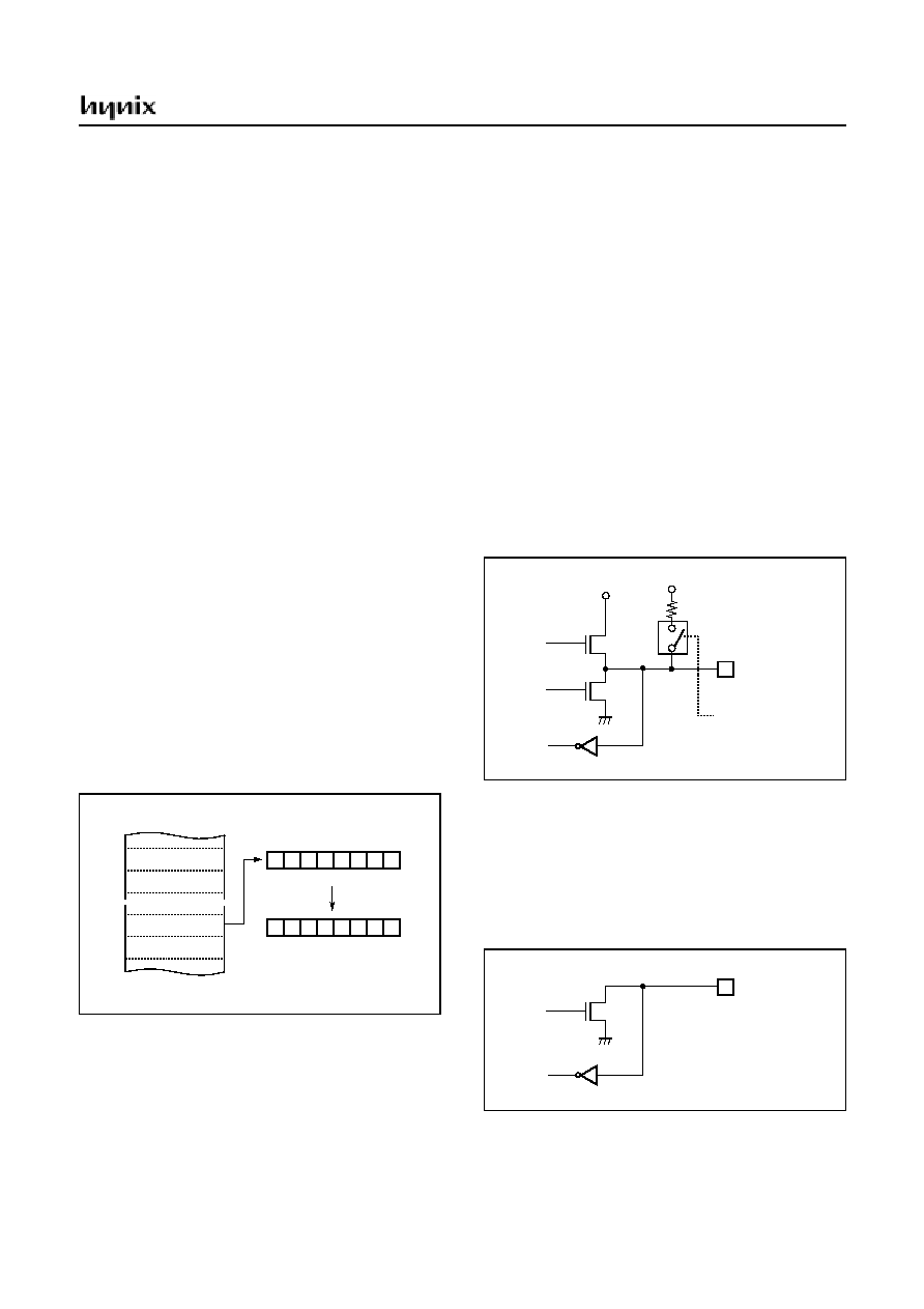
Port Data Registers
The Port Data Registers (R0, R1, R2, R3) are represented
as a D-Type flip-flop, which will clock in a value from the
internal bus in response to a "write to data register" signal
from the CPU. The Q output of the flip-flop is placed on
the internal bus in response to a "read data register" signal
from the CPU. The level of the port pin itself is placed on
the internal bus in response to "read data register" signal
from the CPU. Some instructions that read a port activating
the "read register" signal, and others activating the "read
pin" signal.
Port Direction Registers
All pins have data direction registers which can define
these ports as output or input. A "1" in the port direction
register configure the corresponding port pin as output.
Conversely, write "0" to the corresponding bit to specify it
as input pin. For example, to use the even numbered bit of
R0 as output ports and the odd numbered bits as input
ports, write "55
H
" to address 0C8
H
(R0 port direction reg-
ister) during initial setting as shown in Figure 9-1.
All the port direction registers in the GMS81C5108 have 0
written to them by reset function. On the other hand, its in-
itial status is input.
Figure 9-1 Example of port I/O assignment
Pull-up Control Registers
The R0, R1,R2 and R3 ports have internal pull-up resis-
tors. Figure 9-2 shows a functional diagram of a typical
pull-up port. It is connected or disconnected by Pull-up
Control register (RnPU). The value of that resistor is typi-
cally 100k
. Refer to DC characteristics for more details.
When a port is used as key input, input logic is firmly ei-
ther low or high, therefore external pull-down or pull-up
resisters are required practically. The GMS81C5108 has
internal pull-up, it can be logic high by pull-up that can be
able to configure either connect or disconnect individually
by pull-up control registers RnPU.
When ports are configured as inputs and pull-up resistor is
selected by software, they are pulled to high.
Figure 9-2 Pull-up Port Structure
Open drain port Registers
The R0, R1, R2 and R3 ports have open drain port resistors
R0CR~R3CR.
Figure 9-3 shows an open drain port configuration by control reg-
ister. It is selected as either push-pull port or open-drain port by
R0CR, R1CR, R2CR and R3CR.
Figure 9-3 Open-drain Port Structure
I : INPUT PORT
WRITE "55
H
" TO PORT R0 DIRECTION REGISTER
0
1
0
1
0
1
0
1
I
O
I
O
I
O
I
O
R0 DATA
R0 DIRECTION
R1 DATA
R1 DIRECTION
0C0
H
0C1
H
0C8
H
0C9
H
7
6
5
4
3
2
1
0
BIT
7
6
5
4
3
2
1
0
PORT
O : OUTPUT PORT
~
~
~
~
PULL-UP RESISTOR
PORT PIN
1: Connect
0: Disconnect
Pull-up control bit
VDD
GND
VDD
PORT PIN
1: Open drain
0: Push-pull
Open drain port selection bit
GND
GMS81C5108
32
JUNE 2001 Ver 1.0
9.2 I/O Ports Configuration
R0 Ports
R0 is an 8-bit CMOS bidirectional I/O port (address
0C0
H
). Each I/O pin can independently used as an input or
an output through the R0DR register (address 0C8
H
).
R0 has internal pull-ups that is independently connected or
disconnected by R0PU. The control registers for R0 are
shown below.
In addition, Port R0 and R3 are multiplexed with various
special features. The control register PMR (address 0D9H)
controls the selection of alternate function. After reset, this
value is "0", port may be used as normal I/O port.
To use alternate function such as External Interrupt rather
than normal I/O, write "1" in the corresponding bit of
PMR0.
.
R1 Ports
R1 is an 8-bit CMOS bidirectional I/O port (address
0C1
H
). Each I/O pin can independently used as an input or
an output through the R1DR register (address 0C9
H
).
R1 has internal pull-ups that is independently connected or
disconnected by register R1PU. If the key scan function is
used, these pin can input the key switch signal without ex-
ternal pull-up registers. For more details refer to "18. KEY
SCAN" on page 70.
The control registers for R1 are shown below.
PWMO (PWM Output)
0: R31 Port
1: PWM
R0 Data Register
R0
ADDRESS : 0C0
H
RESET VALUE : 00
H
R07
R06
R05
R04
R03
R02
R01
R00
Port Direction
R0 Direction Register
R0DR
ADDRESS : 0C8
H
RESET VALUE : 00
H
0: Input
1: Output
Pull-up select
R0 Pull-up
R0PU
ADDRESS :0D0
H
RESET VALUE : 00
H
0: Without pull-up
1: With pull-up
Open Drain select
R0 Open Drain
R0CR
ADDRESS :0D4
H
RESET VALUE : 00
H
0: No Open Drain
1: Open Drain
Port Mode Register
PMR
ADDRESS :0D9
H
RESET VALUE : -0-00000
B
-
PWMO
-
BUZ
EC0
INT2
INT1
INT0
BUZ (Buzzer Output)
0: R04 Port
1: BUZ
EC0 (Timer0 Event Input)
0: R03 Port
1: EC0
INT2 (External Interrupt)
0: R02 Port
1: INT2
INT1 (External Interrupt)
0: R01 Port
1: INT1
INT0 (External Interrupt)
0: R00 Port
1: INT0
Selection Register
Selection Register
Port Pin
Alternate Function
R00
R01
R02
R03
R04
R31
INT0 (External Interrupt 0)
INT1 (External Interrupt 1)
INT2 (External Interrupt 2)
EC0 (Timer0 Event Input)
BUZ (Buzzer Output)
PWM (PWM Output)
R1 Data Register
R1
ADDRESS : 0C1
H
RESET VALUE : 00
H
Port Direction
R1 Direction Register
R1DR
ADDRESS : 0C9
H
RESET VALUE : 00
H
0: Input
1: Output
Pull-up select
R1 Pull-up
R1PU
ADDRESS : 0D1
H
RESET VALUE : 00
H
0: Without pull-up
1: With pull-up
R17
R16
R15
R14
R13
R12
R11
R10
Open Drain select
R1 Open Drain
R1CR
ADDRESS :0D5
H
RESET VALUE : 00
H
0: No Open Drain
1: Open Drain
KEY Input select
KEY SCAN Mode Register
KSMR
ADDRESS :0F0
H
RESET VALUE : 00
H
0: Port selection
1: KS selection
Selection Register
Selection Register
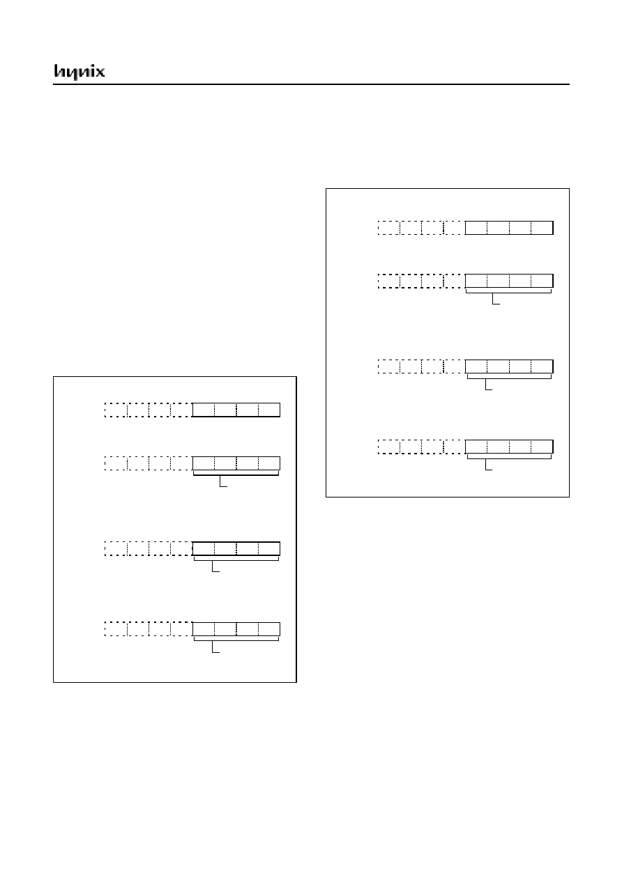
GMS81C5108
JUNE 2001 Ver 1.0
33
Port R1 is multiplexed with various special features.The
control registers controls the selection of alternate func-
tion. After reset, this value is "0", port may be used as nor-
mal I/O port. The way to select alternate function such as
comparator input or buzzer will be shown in each periph-
eral section.
In addition, R1 port is used as key scan function which op-
erate with normal input port.
Input or output is configured automatically by each func-
tion register (KSMR) regardless of R1DR.
R2 Port
R2 is a 4-bit CMOS bidirectional I/O port (address 0C2
H
).
Each I/O pin can independently used as an input or an out-
put through the R2DR register (address 0CA
H
).
R2 has internal pull-ups that is independently connected or
disconnected by R2PU (address 0D2
H
). The control regis-
ters for R2 are shown as below.
R3 Port
R3 is a 4-bit CMOS bidirectional I/O port (address 0C3
H
).
Each I/O pin can independently used as an input or an out-
put through the R3DR register (address 0CB
H
).
SEG0~SEG36
Segment signal output pins for the LCD display. See "19.
LCD DRIVER" on page 71 for details.
COM0~COM3
Common signal output pins for the LCD display. See "19.
LCD DRIVER" on page 71 for details.
SEG34~SEG36 and COM1~COM3 are selected by LCDD
of the LCR register.
R2 Data Register
R2
ADDRESS: 0C2
H
RESET VALUE: ----0000
B
Port Direction
R2 Direction Register
R2DR
ADDRESS : 0CA
H
RESET VALUE : ----0000
B
0: Input
1: Output
Pull-up select
R2 Pull-up
R2PU
ADDRESS : 0D2
H
RESET VALUE : ----0000
B
0: Without pull-up
1: With pull-up
R23
R22
R21
R20
-
-
-
-
-
-
-
-
-
-
-
-
Pull-up select
R2 Open Drain
R2CR
ADDRESS : 0D6
H
RESET VALUE : ----0000
B
0: No Open Drain
1: Open Drain
-
-
-
-
Selection Register
Selection Register
R3 Data Register
R3
ADDRESS: 0C3
H
RESET VALUE: ----0000
B
Port Direction
R3 Direction Register
R3DR
ADDRESS : 0CB
H
RESET VALUE : ----0000
B
0: Input
1: Output
Pull-up select
R3 Pull-up
R3PU
ADDRESS : 0D3
H
RESET VALUE : ----0000
B
0: Without pull-up
1: With pull-up
R33
R32
R31
R30
-
-
-
-
-
-
-
-
-
-
-
-
Pull-up select
R3 Open Drain
R3CR
ADDRESS : 0D7
H
RESET VALUE : ----0000
B
0: No Open Drain
1: Open Drain
-
-
-
-
Selection Register
Selection Register
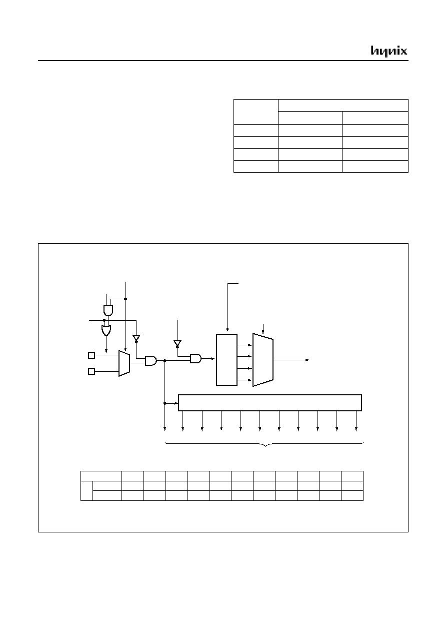
GMS81C5108
34
JUNE 2001 Ver 1.0
10. CLOCK GENERATOR
As shown in Figure 10-1, the clock generator produces the
basic clock pulses which provide the system clock to be
supplied to the CPU and the peripheral hardware. It con-
tains two oscillators: a main-frequency clock oscillator and
a sub-frequency clock oscillator. Power consumption can
be reduced by switching them to the low power operation
frequency clock can be easily obtained by attaching a res-
onator between the X
IN
and X
OUT
pin and the SX
IN
and
SX
OUT
pin, respectively. The system clock can also be ob-
tained from the external oscillator.
The clock generator produces the system clocks forming
clock pulse, which are supplied to the CPU and the periph-
eral hardware. The internal system clock can be selected
by bit2, and bit3 of the system clock mode register (SC-
MR). The registers are shown in Figure 10-2.
To the peripheral block, the clock among the not-divided
original clocks, divided by
2
, 4,...,
up to 1024 can be pro-
vided. Peripheral clock is enabled or disabled by STOP in-
struction. The peripheral clock is controlled by clock
control register (CKCTLR). See "11. BASIC INTERVAL
TIMER" on page 43 for details.
Figure 10-1 Block Diagram of Clock Generator
CPU clock
Instruction cycle time
f
MAIN
= 4MHz
f
SUB
= 32.768kHz
÷
2
0.5 us
61 us
÷
8
2.0 us
244 us
÷
16
4.0 us
488 us
÷
64
16.0 us
1953 us
Internal system clock
SX
IN
PRESCALER
0
1
X
IN
÷
1
Peripheral clock
MUX
÷
2
÷
4
÷
8
÷
16
÷
128
÷
256
÷
512
÷
1024
÷
32
÷
64
÷
2
÷
8
÷
16
÷
64
select clock
SCS[1:0]
OSC Stop
SYCC<1>
SYCC<0>
STOP Mode
SLEEP Mode
PS0
PS1
PS2
PS3
PS4
PS5
PS6
PS7
PS8
PS9
PS10
** Clock is frozen by STOP or SLEEP[SMR.0] Instruction.
** Clock is released
1) by BIT overflow when previos state has been STOP mode.
2) by interrupts when previos state has been SLEEP mode.
PRES
CAL
E
R
f
EX
(Hz)
PS0
PS3
PS2
PS4
PS1
PS10
PS9
PS5
PS6
PS7
4M
Frequency
period
4M
1M
500K
250K
2M
125K
62.5K
250n
500n
1u
2u
4u
8u
16u
32u
64u
256u
128u
3.906K
7.183K
15.63K
31.25K
PS8
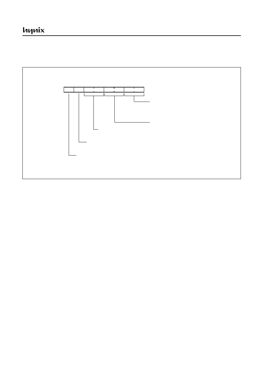
GMS81C5108
JUNE 2001 Ver 1.0
35
The system clock is decided by bit1 of the system clock
mode register, SCMR. In selection Sub clock, to oscillate
or stop the Main clock is decided by bit0 of SCMR.
On the initial reset, internal system clock is PS1 which is
the fastest and other clock can be provided by bit2 and bit3
of SCMR.
Figure 10-2 SCMR : System Clock Control Registers
R/W
R/W
R/W
R/W
SYCC[1:0] (System clock control)
00: main clock on
01: main clock on
10: sub clock on (main clock on)
11: sub clock on (main clock off)
SCS[1:0] (System clock source select)
00: f
MAIN
÷
2
01: f
MAIN
÷
8
INITIAL VALUE: 00
H
ADDRESS: 0F5
H
SCMR (System Clock Mode Register)
10: f
MAIN
÷
16
11: f
MAIN
÷
64
MSB
LSB
or f
SUB
÷
2
or f
SUB
÷
8
or f
SUB
÷
16
or f
SUB
÷
64
R/W
R/W
R/W
R
SVD[1:0] (SVD Flag)
SVD0 : set at VDD=2.2V
SVD1 : set at VDD=1.7V
SVRT (System Reset Control by SVD1 Bit)
0 : System reset by SVD1 Flag
1 : Don't system reset by SVD1 Flag (Freeze)
SVEN (SVD Operation Enable Bit)
0 : SVD Operation Enable
1 : SVD Operation Disable
* The values of 1.7V and 2.2V could be changed by ±0.2V according to the process of work.
GMS81C5108
36
JUNE 2001 Ver 1.0
10.1 Operation Mode
The system clock controller starts or stops the main-fre-
quency clock oscillator and switches between the sub fre-
quency clock. The operating mode is generally divided
into the main active mode and the sub active mode, which
are controlled by System clock mode register (SCMR).
Figure 10-3 shows the operating mode transition diagram.
System clock control is performed by the system clock
mode register, SCMR. During reset, this register is initial-
ized to "0" so that the main-clock operating mode is select-
ed.
Main Active mode
This mode is fast-frequency operating mode.
The CPU and the peripheral hardwares are operated on the
high-frequency clock. At reset release, this mode is in-
voked.
Sub Active mode
This mode is low-frequency operating mode
In this mode, the CPU and the peripheral hardware clock
are provided by low-frequency clock oscillation, so power
consumption can be reduced.
SLEEP mode
In this mode, the CPU clock stops while peripherals and
the oscillation source continue to operate normally.
STOP mode
In this mode, the system operations are all stopped, holding
the internal states valid immediately before the stop at the
low power consumption level.
Figure 10-3 Operating Mode
Main Active
Mode
Main : Stop or Oscillation (case of **1)
Sub : Oscillation
Main : Oscillation
Sub : Oscillation
Sub Active
Mode 1
Sub Active
Mode 2
Stop / Sleep
Mode
*
No
te
1
/
*
No
te
2
System Clock : Main
Main : Oscillation
Sub : Oscillation
System Clock : Sub
SET1 SCMR.1
CLR1 SCMR.1
*
N
ot
e3
* No
te1
/
N
ot
e2
ST
O
P /
(**
1)
S
E
T1 S
MR
.0
LD
M SCM
R,
#0
3H
ST
O
P
/
SET
1
SM
R.0
CLR1 SCM
R
.
0
SET
1
SCMR.
0
* Note1 / * Note2
STOP / SET1 SMR.0
System Clock : Stop
Main : Stop
Sub : Oscillation
System Clock : Sub
* Note1 : Stop released by
Reset, Key Scan
Watch Timer interrupt
Timer interrupt (event counter)
SIO (External clock)
External interrupt
* Note2 : Sleep released by
Reset, Key Scan
All interrupts
* Note3 : this is sequential
1) CLR1 SCMR.0
2) Oscillation stabilation time (more than 65ms)
3) CLR1 SCMR.1
- Sub clock cannot be stopped by STOP instruction.

GMS81C5108
JUNE 2001 Ver 1.0
37
10.2 Operation Mode Switching
In the Main active mode, only the high-frequency clock os-
cillator is used.
In the Sub active mode, the low-frequency clock oscilla-
tion is used, so the low power voltage operation or the low
power consumption operation can be enabled. Instruction
execution does not stop during the change of operation
mode. In this case, some peripheral hardware capabilities
may be affected. For details, refer to the description of the
relevant operation.
The following describes the switching between the Main
active mode and the Sub active mode. During reset, the
system clock mode register is initialized at the Main active
mode. It must be set to the Sub active mode for reducing
the power consumption.
Switching from Main active to Sub active
First, write "02
H"
into lower 2 bits of SCMR to switch the
main system clock to the sub-frequency clock.
Next, write "03
H"
to turn off main frequency oscillation.
Example:
:
:
:
LDM SCMR,#02
H
;Switch to sub active
LDM SCMR,#03
H
;Turn off main clock
:
:
Returning from Sub active to Main active
First, write "02
H"
into lower 2 bits of the SCMR to turn on
the main-frequency oscillation. This time, the stabilization
(warm-up) time needs to be taken by the software delay
routine. Sub active mode can also be released by setting the
RESET pin to low, which immediately performs the reset
operation. After reset, the GMS81C5108 is placed in Main
active mode.
Example:
:
:
:
LDM SCMR,#02
H
;Turn on main-clock
CALL DELAY ;Wait until stable
LDM SCMR,#0 ;Move to main active
:
:
:
;about 65ms software delay
DELAY:
LDA
#0
DELAY0:
INC
A
CMP
#85H
BCC
DELAY0
RET
Shifting from the Normal operation to the SLEEP
mode
By setting bit 0 of SMR, the CPU clock stops and the
SLEEP mode is invoked. The CPU stops while other pe-
ripherals are operate normally.
The way of release from this mode is RESET and all avail-
able interrupts.
For more detail, See " SLEEP Mode" on page 39
Shifting from the Normal operation to the STOP
mode
By executing STOP instruction, the main-frequency clock
oscillation stops and the STOP mode is invoked. But sub-
frequency clock oscillation is operated continuously.
After the STOP operation is released by reset, the opera-
tion mode is changed to Main active mode.
The methods of release are RESET, Key scan interrupt,
Watch Timer interrupt, Timer/Event counter1 (EC0 pin),
SIO (External clock) and External Interrupt.
For more details, see " STOP Mode" on page 40.
Note: In the STOP and SLOW operating modes, the power
consumption by the oscillator and the internal hardware is
reduced. However, the power for the pin interface (depend-
ing on external circuitry and program) is not directly associ-
ated with the low-power consumption operation. This must
be considered in system design as well as interface circuit
design.
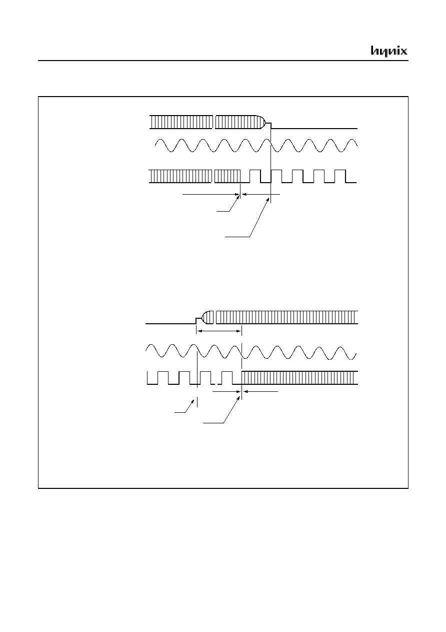
GMS81C5108
38
JUNE 2001 Ver 1.0
Figure 10-4 System Clock Switching Timing
Operation clock
~~
~~
Sub-clock operation
Main-clock operation
Sub freq. clock
Main freq. clock
(X
IN
pin)
(SX
IN
pin)
Changed to the Sub-clock
SCMR
XXXX XX10
B
~~
~~
~~
Operation clock
~~
Main-clock operation
Stabilizing Time
>
60ms
Sub freq. clock
Main freq. clock
(X
IN
pin)
(SX
IN
pin)
Changed to the Transition
Changed to the Main-clock
SCMR
XXXX XX10
B
SCMR
XXXX XX00
B
~~
~~
Sub-clock operation
~~
(a) Main active mode
Sub active mode
(b) Sub active mode
Main active mode
or XXXX XX01
B
Turn off main clock
SCMR
XXXX XX11
B
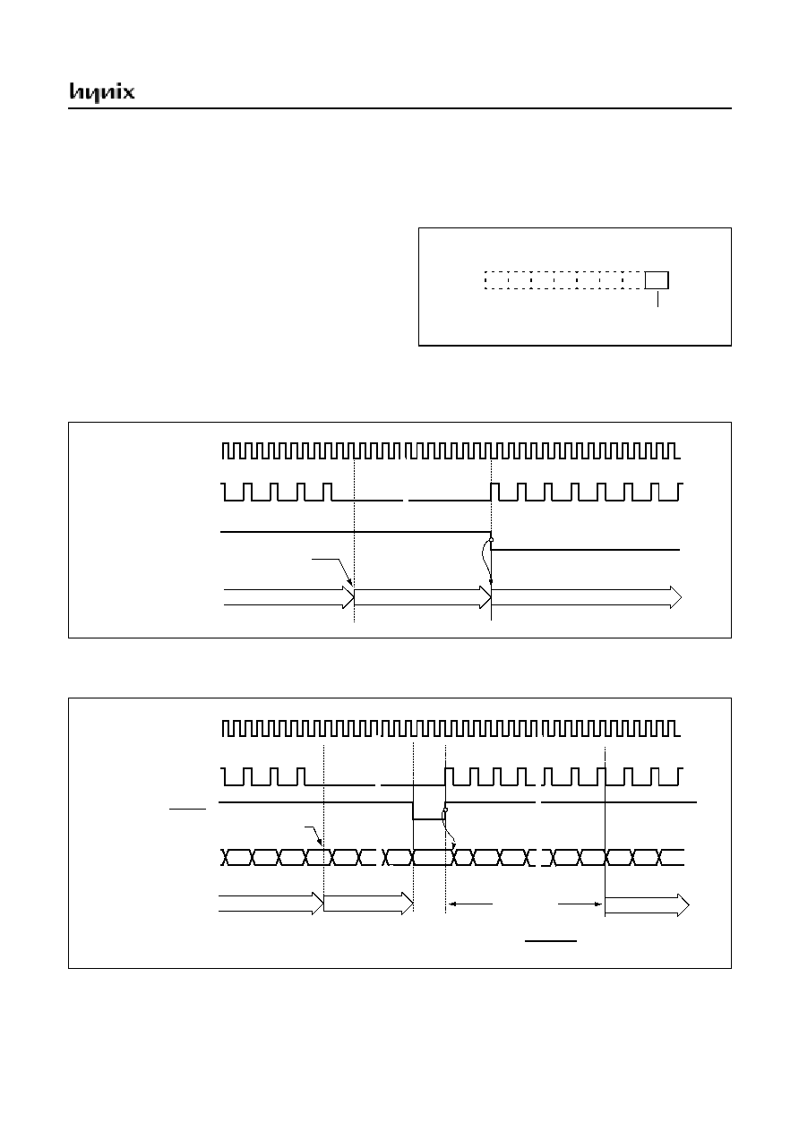
GMS81C5108
JUNE 2001 Ver 1.0
39
10.3 Power Saving Operation
GMS81C5108 has 2 power-saving mode. In power-saving
mode, power consumption is reduced considerably that in
Battery operation Battery life can be extended a lot.
Sleep mode is entered by setting bit 0 of Sleep Mode Reg-
ister (SMR), and STOP Mode is entered by STOP instruc-
tion.
SLEEP Mode
In this mode, the internal oscillation circuits remain active.
Oscillation continues and peripherals are operate normally
but CPU stops. Movement of all Peripherals is shown in
Table 10-1. Sleep mode is entered by setting bit 0 of SMR
(address 0DE
H
).
It is released by RESET or interrupt. To be released by in-
terrupt, interrupt should be enabled before Sleep mode.
Figure 10-5 SLEEP Mode Register
Figure 10-6 Sleep Mode Release Timing by External Interrupt
.
Figure 10-7 SLEEP Mode Release Timing by RESET pin
Sleep Mode Register
SMR
ADDRESS : 0DE
H
RESET VALUE : -------0
B
0: Release Sleep Mode
1: Enter Sleep Mode
-
-
-
-
-
-
-
Oscillator
Normal Operation
Stand-by Mode
Normal Operation
Interrupt
Internal CPU Clock
Release
Set bit 0 of SMR
(X
IN
or SX
IN
pin)
~~
~~
Oscillator
(X
IN
or SX
IN
pin)
0
BIT Counter
1
FE
FF
0
1
2
~~
t
ST
= 62.5ms
~~
~~
RESET
Internal CPU Clock
Clear & Start
~~
~~
Normal Operation
Stand-by Mode
Normal Operation
Release
Set bit 0 of SMR
~~
~~
~~
at 4.19MHz by hardware
~~
2
t
ST
=
x 256
f
MAIN
÷
1024
1
GMS81C5108
40
JUNE 2001 Ver 1.0
STOP Mode
For applications where power consumption is a critical
factor, device provides STOP mode for reducing power
consumption.
Start The Stop Operation
The STOP mode can be entered by STOP instruction dur-
ing program execution. In Stop mode, the on-chip main-
frequency oscillator, system clock, and peripheral clock
are stopped (Watch timer clock is oscillating continuous-
ly:. With the clock frozen, all functions are stopped, but the
on-chip RAM and Control registers are held. The port pins
output the values held by their respective port data register,
the port direction registers. The status of peripherals during
Stop mode is shown below.
Table 10-2 Clock Operation of STOP and SLEEP mode
Note: Since the X
IN
pin is connected internally to GND to
avoid current leakage due to the crystal oscillator in STOP
mode, do not use STOP instruction when an external clock
is used as the main system clock.
In the Stop mode of operation, V
DD
can be reduced to min-
imize power consumption. Be careful, however, that V
DD
is not reduced before the Stop mode is invoked, and that
V
DD
is restored to its normal operating level before the
Stop mode is terminated.
The reset should not be activated before V
DD
is restored to
its normal operating level, and must be held active long
enough to allow the oscillator to restart and stabilize.
And after STOP instruction, at least two or more NOP in-
struction should be written as shown in example below.
Peripheral
STOP Mode
Sleep Mode
CPU
All CPU operations are disabled
All CPU operations are disabled
RAM
Retain
Retain
LCD driver
Operates continuously
Operates continuously
Basic Interval Timer
Halted
Operates continuously
Timer/Event counter 0,1
Halted (Only when the Event counter mode
is enabled, Timer 0,1 operates normally)
Timer/Event counter 0,1 operates continuously
Watch Timer
Operates continuously
Operates continuously
Key Scan
Active
Active
Main-oscillation
Stop (X
IN
=L, X
OUT
=L)
Oscillation
1
Sub-oscillation
Oscillation
Oscillation
I/O ports
Retain
Retain
Control Registers
Retain
Retain
Release method
by RESET, Key Scan interrupt,
SIO interrupt, Watch Timer interrupt,
Timer interrupt (EC0), and External interrupt
by RESET, All interrupts
Table 10-1 Peripheral Operation during Power Saving Mode
1. refer to the Table 10-2
Operating
Clock source
Main
Operating Mode
Main
Sleep Mode
Sub
Operating Mode
Sub
Sleep Mode
Stop Mode
Main Clock
Oscillation
Oscillation
SCMR<1:0>
00,01,10
Oscillation
11
Stop
SCMR<1:0>
00,01,10
Oscillation
11
Stop
Stop
Sub Clock
Oscillation
Oscillation
Oscillation
Oscillation
Oscillation
System Clock
Active
Stop
Active
Stop
Stop
Peri. Clock
Active
Active
Active
Active
Stop
GMS81C5108
JUNE 2001 Ver 1.0
41
Example)
:
LDM
CKCTLR,#0000_1111B
STOP
NOP
NOP
:
The Interval Timer Register CKCTLR should be initial-
ized by software in order that oscillation stabilization time
should be longer than 20ms before STOP mode.
Release the STOP mode
The exit from STOP mode is using hardware reset or exter-
nal interrupt, watch timer, SIO interrupt, key scan or timer
interrupt (EC0).
To release STOP mode, corresponding interrupt should be
enabled before STOP mode.
Specially as a clock source of Timer/Event counter, EC0
pin can release it by Timer/Event counter
Interrupt re-
quest
Reset redefines all the control registers but does not change
the on-chip RAM. External interrupts allow both on-chip
RAM and Control registers to retain their values.
Start-up is performed to acquire the time for stabilizing os-
cillation. During the start-up, the internal operations are all
stopped.
Figure 10-8 STOP Mode Release Timing by External Interrupt
Figure 10-9 STOP Mode Release Timing by RESET
Before executing Stop instruction, Basic Interval Timer must be set
Oscillator
(X
IN
pin)
~~
n
0
BIT Counter
n+1
n+2
n+3
~~
Normal Operation
Stop Operation
Normal Operation
1
FE
FF
0
1
2
~~
~~
~~
t
ST
>
20ms
~~
~~
External Interrupt
Internal Clock
Clear
STOP Instruction
Executed
~~
~~
~~
properly by software to get stabilization time which is longer than 20ms.
by software
~~
Oscillator
(X
IN
pin)
~~
n
0
BIT Counter
n+1
n+2
n+4
~~
Normal Operation
Stop Operation
Normal Operation
1
FE
FF
0
1
2
~~
~~
~~
t
ST
> 62.5ms
Internal Clock
Clear
STOP Instruction
Executed
~~
~~
~~
at 4.19MHz by hardware
~~
RESET
n+3
t
ST
=
x 256
f
MAIN
÷
1024
1
~~
~~
GMS81C5108
42
JUNE 2001 Ver 1.0
Minimizing Current Consumption
The Stop mode is designed to reduce power consumption.
To minimize current drawn during Stop mode, the user
should turn-off output drivers that are sourcing or sinking
current, if it is practical.
Note: In the STOP operation, the power dissipation asso-
ciated with the oscillator and the internal hardware is low-
ered; however, the power dissipation associated with the
pin interface (depending on the external circuitry and pro-
gram) is not directly determined by the hardware operation
of the STOP feature. This point should be little current flows
when the input level is stable at the power voltage level
(V
DD
/V
SS
); however, when the input level becomes higher
than the power voltage level (by approximately 0.3V), a cur-
rent begins to flow. Therefore, if cutting off the output tran-
sistor at an I/O port puts the pin signal into the high-
impedance state, a current flow across the ports input tran-
sistor, requiring it to fix the level by pull-up or other means.
It should be set properly that current flow through port
doesn't exist.
First consider the setting to input mode. Be sure that there
is no current flow after considering its relationship with
external circuit. In input mode, the pin impedance viewing
from external MCU is very high that the current doesn't
flow.
But input voltage level should be V
SS
or V
DD
. Be careful
that if unspecified voltage, i.e. if unfirmed voltage level
(not V
SS
or V
DD
) is applied to input pin, there can be little
current (max. 1mA at around 2V) flow.
If it is not appropriate to set as an input mode, then set to
output mode considering there is no current flow. Setting
to High or Low is decided considering its relationship with
external circuit. For example, if there is external pull-up re-
sistor then it is set to output mode, i.e. to High, and if there
is external pull-saving register, it is set to low.
Figure 10-10 Application Example of Unused Input Port
Figure 10-11 Application Example of Unused Output Port
INPUT PIN
V
DD
GND
i
V
DD
X
Weak pull-up current flows
V
DD
internal
pull-up
INPUT PIN
i
V
DD
X
Very weak current flows
V
DD
O
O
OPEN
OPEN
i=0
O
i=0
O
GND
When port is configured as an input, input level should
be closed to 0V or V
DD
to avoid power consumption.
OUTPUT PIN
GND
i
In the left case, much current flows from port to GND.
X
ON
OFF
OUTPUT PIN
GND
i
In the left case, Tr. base current flows from port to GND.
i=0
X
OFF
ON
V
DD
L
ON
OFF
OPEN
GND
V
DD
L
ON
OFF
To avoid power consumption, there should be low output
ON
OFF
O
O
V
DD
O
to the port.
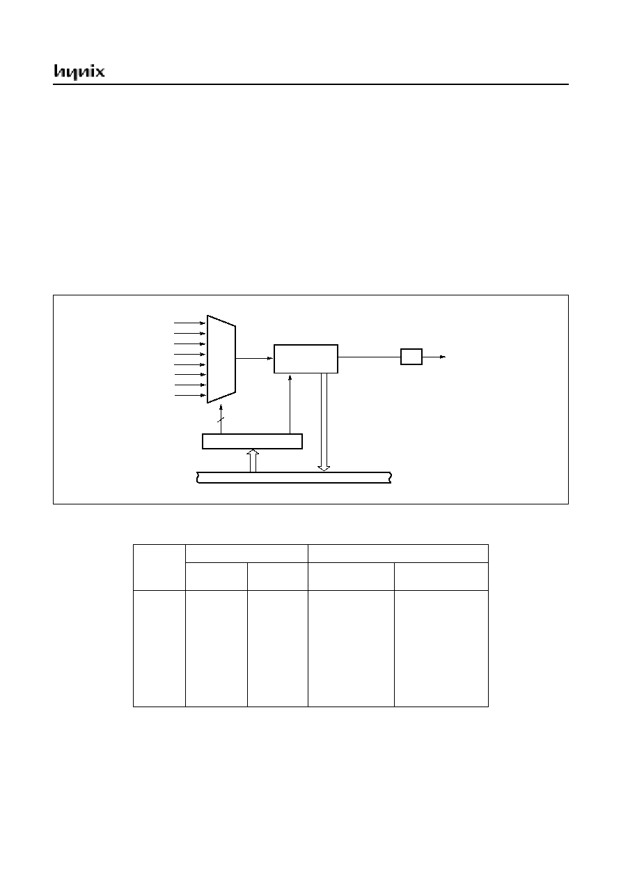
GMS81C5108
JUNE 2001 Ver 1.0
43
11. BASIC INTERVAL TIMER
The GMS81C5108 has one 8-bit Basic Interval Timer that
is free-run and can not stop. Block diagram is shown in
Figure 11-1.
The Basic Interval Timer Register (BITR) is increased ev-
ery internal count pulse which is divided by prescaler.
Since prescaler has divided ratio by 8 to 1024, the count
rate is 1/8 to 1/1024 of the oscillator frequency. After reset,
the BCK bits are all set, so the longest oscillation stabiliza-
tion time is obtained.
It also provides a Basic interval timer interrupt (BITF).
The count overflow of BITR from FF
H
to 00
H
causes the
interrupt to be generated. The Basic Interval Timer is con-
trolled by the clock control register (CKCTLR) shown in
Figure 11-2.
Source clock can be selected by lower 3 bits of CKCTLR.
When write "1" to bit BCL of CKCTLR, BITR register is
cleared to "0" and restart to count up. The bit BCL be-
comes "0" automatically after one machine cycle by hard-
ware.
BITR and CKCTLR are located at same address, and ad-
dress 0F4
H
is read as a BITR, and written to CKCTLR.
Figure 11-1 Block Diagram of Basic Interval Timer
Table 11-1 Basic Interval Timer Interrupt Time
MUX
Basic Interval Timer Interrupt
BITR
Select Input clock
3
Basic Interval Timer
source
clock
8-bit up-counter
BCK<2:0>
BCL
f
MAIN
÷
2
10
or f
SUB
÷
2
10
f
MAIN
÷
2
9
or f
SUB
÷
2
9
f
MAIN
÷
2
8
or f
SUB
÷
2
8
f
MAIN
÷
2
7
or f
SUB
÷
2
7
f
MAIN
÷
2
6
or f
SUB
÷
2
6
f
MAIN
÷
2
5
or f
SUB
÷
2
5
f
MAIN
÷
2
4
or f
SUB
÷
2
4
f
MAIN
÷
2
3
or f
SUB
÷
2
3
CKCTLR
clear
overflow
Internal bus line
clock control register
[0F4
H
]
[0F4
H
]
BITF
f
MAIN
: main-clock frequency
f
SUB
: sub-clock frequency
BCK
<2:0>
Source clock
Interrupt (overflow) Period
SC M R [1:0]=
00 or 01
SC M R [1:0]=
10 or 11
At f
MAIN
=4MHz
At f
SUB
=32.768kHz
000
001
010
011
100
101
110
111
f
MAIN
÷
2
3
f
MAIN
÷
2
4
f
MAIN
÷
2
5
f
MAIN
÷
2
6
f
MAIN
÷
2
7
f
MAIN
÷
2
8
f
MAIN
÷
2
9
f
MAIN
÷
2
10
f
SUB
÷
2
3
f
SUB
÷
2
4
f
SUB
÷
2
5
f
SUB
÷
2
6
f
SUB
÷
2
7
f
SUB
÷
2
8
f
SUB
÷
2
9
f
SUB
÷
2
10
0.512
1.024
2.048
4.096
8.192
16.384
32.768
65.536
ms
62.5
125.0
250.0
500.0
1000.0
2000.0
4000.0
8000.0
ms
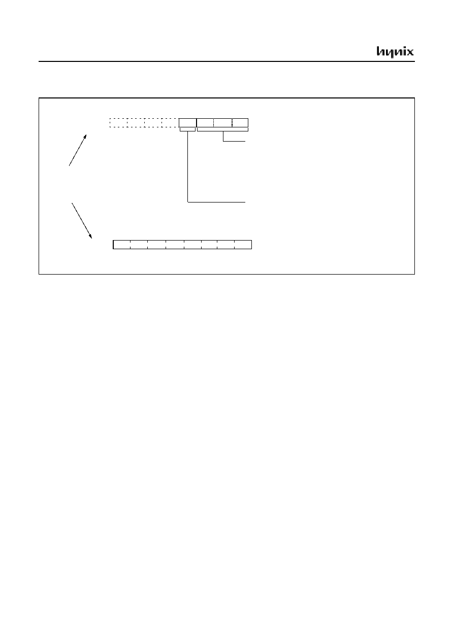
GMS81C5108
44
JUNE 2001 Ver 1.0
Figure 11-2 BITR: Basic Interval Timer Mode Register
Example 1:
Interrupt request flag is generated every 8.192ms at 4MHz.
:
LDM
CKCTLR,#0CH
SET1
BITE
EI
:
BCL
7
6
5
4
3
2
1
0
-
-
-
BCK1
Basic Interval Timer source clock select
000: f
MAIN
÷
2
3
001: f
MAIN
÷
2
4
010: f
MAIN
÷
2
5
011: f
MAIN
÷
2
6
100: f
MAIN
÷
2
7
101: f
MAIN
÷
2
8
110: f
MAIN
÷
2
9
111: f
MAIN
÷
2
10
Clear bit
0: Normal operation (free-run)
1: Clear 8-bit counter (BITR) to "0". This bit becomes 0 automatically
INITIAL VALUE: ----0111
B
ADDRESS: 0F4
H
after one machine cycle.
CKCTLR
7
6
5
4
3
2
1
0
INITIAL VALUE: 00
H
ADDRESS: 0F4
H
BITR
Both register are in same address,
when write, to be a CKCTLR,
when read, to be a BITR.
Caution:
8-BIT BINARY COUNTER
-
f
MAIN
: main-clock frequency
f
SUB
: sub-clock frequency
BCK0
BCK2
or f
SUB
÷
2
4
or f
SUB
÷
2
3
or f
SUB
÷
2
6
or f
SUB
÷
2
5
or f
SUB
÷
2
7
or f
SUB
÷
2
9
or f
SUB
÷
2
8
or f
SUB
÷
2
10

GMS81C5108
JUNE 2001 Ver 1.0
45
12. Timer / Counter
Timer/Event Counter consists of prescaler, multiplexer, 8-
bit timer data register, 8-bit counter register, mode register,
input capture register and Comparator as shown in Figure
12-3. And the PWM high register for PWM is consisted
separately.
The timer/counter has seven operating modes.
- 8 Bit Timer/Counter Mode
- 8 Bit Capture Mode
- 8 Bit Compare Output Mode
- 16 Bit Timer/Counter Mode
- 16 Bit Capture Mode
- 16 Bit Compare Output Mode
- PWM Mode
In the "timer" function, the register is increased every in-
ternal clock input. Thus, one can think of it as counting in-
ternal clock input. Since a least clock consists of 2 and
most clock consists of 1024 oscillator periods, the count
rate is 1/2 to 1/1024 of the oscillator frequency in Timer0.
And Timer1 can use the same clock source too. In addition,
Timer1 has more fast clock source (1/1 to 1/8).
In the "counter" function, the register is increased in re-
sponse to a 0-to-1 (rising edge) transition at its correspond-
ing external input pin EC0 (Timer 0).
In addition the "capture" function, the register is increased
in response external interrupt same with timer function.
When external interrupt edge input, the count register is
captured into capture data register CDRx.
Timer1 is shared with "PWM" function and "Compare
output" function.
Example 1:
Timer 0 = 8-bit timer mode, 8ms interval at 4MHz
Timer 1 = 8-bit timer mode, 4ms interval at 4MHz
LDM SCMR,#0 ;Main clock mode
LDM TDR0,#249
LDM TM0,#0001_0011B
LDM TDR1,#124
LDM TM1,#0000_1111B
SET1 T0E
SET1 T1E
EI
:
:
:
Example 2:
Timer0 = 16-bit timer mode, 0.5s at 4MHz
LDM SCMR,#0 ;Main clock mode
LDM TDR0,#23H
LDM TDR1,#0F4H
LDM TM0,#0FH ;F
MAIN
/32, 8us
LDM TM1,#4CH
SET1 T0E
EI
:
:
:
Example 3:
Timer0 = 8-bit event counter, 2ms interval at 4MHz
Timer1 = 8-bit capture mode, 2us sampling count.
LDM TDR0,#99 ;99+1, 100 count
LDM TM0,#01FH ;event counter
LDM R0DR,#XXXX_1XXXB ;R03input
LDM IESR,#XXXX_01XXB ;FALLING
LDM PMR,#XXXX_1X1XB ;EC0,INT1
LDM TDR1,#0FFH
LDM TM1,#0001_1011B ;2us
SET1 T0E;ENABLE TIMER 0
SET1 T1E;ENABLE TIMER 1
SET1 INT1E;ENABLE EXT. INT1
EI
:
X: don't care.
Example 4:
Timer0 = 16-bit capture mode, 8us sampling count. at 4MHz
LDM TDR0,#0FFH
LDM TDR1,#0FFH
LDM TM0,#02FH
LDM TM1,#04FH
LDM IESR,#XXXX_XX01B
LDM PMR,#XXXX_XXX1B ;AS INT0
SET1 T0E;ENABLE TIMER 0
SET1 INT0E;ENABLE EXT. INT0
EI
:
X: don't care.

GMS81C5108
46
JUNE 2001 Ver 1.0
Figure 12-1 Timer0,1 Registers
T0CK2
Bit : 7 6 5 4 3 2 1 0
CAP0
-
-
T0CK[2:0] (Timer 0 Input Clock Selection)
111: External Event clock (EC0)
T0CN (Timer 0 Continue Start)
0: Stop Counting
1: Start Counting
T0ST (Timer 0 Start Control)
0: stop counting
1: clear the counter and start count again
Reserved
INITIAL VALUE:--000000
B
ADDRESS: 0E0
H
TM0 (Timer0 Mode Register)
R/W
R/W
R/W
R/W
T0CN
T0ST
T0CK1
T0CK0
R/W
R/W
CAP0 (Capture Mode Selection Bit)
0: Capture Disable
1: Capture Enable
CAP1
Bit : 7 6 5 4 3 2 1 0
PWME
T1CK[1:0] (Timer 1 Input Clock Selection)
11: Timer 0 Clock
T1CN (Timer 1 Continue Start)
0: Stop Counting
1: Start Counting
T1ST (Timer 1 Start Control)
0: stop counting
1: clear the counter and start count again
INITIAL VALUE:00000000
B
ADDRESS: 0E2
H
TM1 (Timer1 Mode Register)
R/W
R/W
R/W
R/W
T1CN
T1ST
T1CK1
T1CK0
R/W
R/W
POL (PWM Output Polarity Selection)
0: Duty Active Low
1: Duty Active High
POL
16BIT
R/W
R/W
CAP1 (Capture Mode Selection Bit)
0: Capture Disable
1: Capture Enable
PWME (PWM Enable Bit)
0: PWM Disable
1: PWM Enable
16BIT (16 Bit Mode Selection)
0: 8-Bit Mode
1: 16-Bit Mode
**The counter will be cleared and restarted only when the TxST bit cleared and set again.
If TxST bit set again when TxST bit is set, the counter can't be cleared but only start again.
000: f
MAIN
÷
2
001: f
MAIN
÷
2
2
010: f
MAIN
÷
2
3
011: f
MAIN
÷
2
5
100: f
MAIN
÷
2
7
101: f
MAIN
÷
2
9
110: f
MAIN
÷
2
10
f
MAIN
: main-clock frequency
f
SUB
: sub-clock frequency
or f
SUB
÷
2
2
or f
SUB
÷
2
or f
SUB
÷
2
5
or f
SUB
÷
2
3
or f
SUB
÷
2
7
or f
SUB
÷
2
10
or f
SUB
÷
2
9
00: f
MAIN
01: f
MAIN
÷
2
10: f
MAIN
÷
2
3
or f
SUB
÷
2
or f
SUB
or f
SUB
÷
2
3
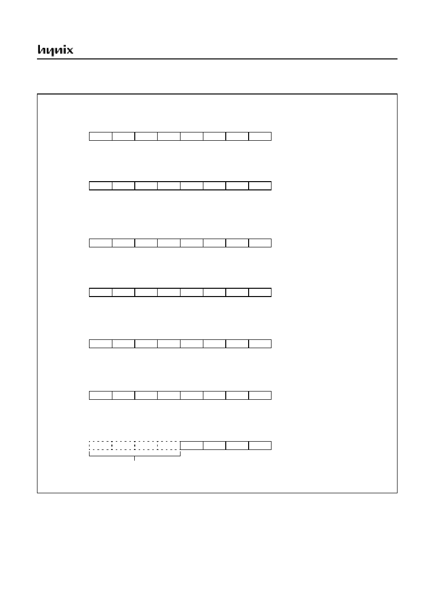
GMS81C5108
JUNE 2001 Ver 1.0
47
Figure 12-2 Related Registers with Timer/Counter
CDR0 (Input Capture Register)
T0 (Timer 0 Counter Register)
CDR04
Bit : 7 6 5 4 3 2 1 0
CDR05
INITIAL VALUE:00H
ADDRESS: E1
H
R
R
R
R
CDR01
CDR00
CDR03
CDR02
R
R
In Timer mode, this register is the value of Timer 0 counter and in Capture mode, this register is the value of input capture.
CDR07
CDR06
R
R
TDR0 (Timer 0 Data Register)
TDR04
Bit : 7 6 5 4 3 2 1 0
TDR05
INITIAL VALUE:FF
H
ADDRESS: 0E1
H
W
W
W
W
TDR01
TDR00
TDR03
TDR02
W
W
If the counter of Timer 0 and the data of TDR0 is equal, interrupt is occurred.
TDR07
TDR06
W
W
CDR1 (Input Capture Register)
T1 (Timer 1 Counter Register)
CDR14
Bit : 7 6 5 4 3 2 1 0
CDR15
INITIAL VALUE:00
H
ADDRESS: 0E4
H
R
R
R
R
CDR11
CDR10
CDR13
CDR12
R
R
In Timer mode, this register is the value of Timer 1 counter and in Capture mode, this register is the value of input capture.
CDR17
CDR16
R
R
TDR1 (Timer 1 Data Register)
TDR14
Bit : 7 6 5 4 3 2 1 0
TDR15
INITIAL VALUE:FF
H
ADDRESS: 0E3
H
W
W
W
W
TDR11
TDR10
TDR13
TDR12
W
W
If the counter of Timer 1 and the data of TDR1 is equal, interrupt is occurred.
TDR17
TDR16
W
W
T1PPR (Timer 1 Pulse Period Register)
T1PPR4
Bit : 7 6 5 4 3 2 1 0
T1PPR5
INITIAL VALUE:FF
H
ADDRESS: 0E3
H
W
W
W
W
T1PPR1 T1PPR0
T1PPR3 T1PPR2
W
W
The period is decided by PWM.
T1PPR7 T1PPR6
W
W
T1PDR (Timer 1 Pulse Duty Register)
T1PDR4
Bit : 7 6 5 4 3 2 1 0
T1PDR5
INITIAL VALUE:00
H
ADDRESS: 0E4
H
W/R
W/R
W/R
W/R
T1PDR1 T1PDR0
T1PDR3 T1PDR2
W/R
W/R
In PWM mode, decide the pulse duty.
T1PDR7 T1PDR6
W/R
W/R
PWMHR (PWM High Register)
-
Bit : 7 6 5 4 3 2 1 0
-
INITIAL VALUE:----0000
B
ADDRESS: 0E5
H
W
W
W
W
PWM01
PWM00
PWM03 PWM02
PWM Period = [PWMHR[3:2] + T1PPR] x Source Clock
-
-
Reserved
PWM Duty = [PWMHR[1:0] + T1PDR] x Source Clock
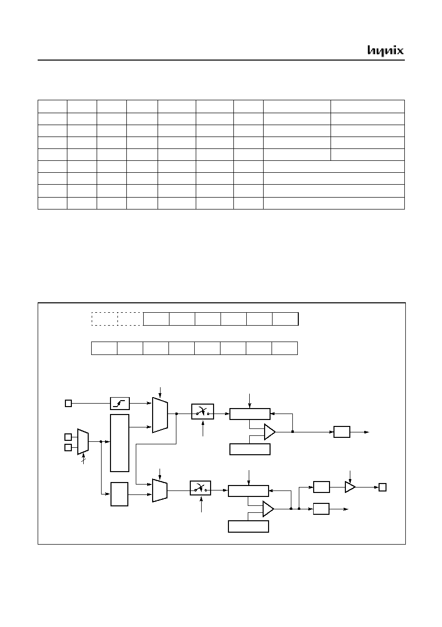
GMS81C5108
48
JUNE 2001 Ver 1.0
Table 12-1 Operating Modes of Timer 0 and Timer 1
12.1 8-Bit Timer/Counter Mode
The GMS81C5108 has two 8-bit Timer/Counters, Timer 0,
Timer 1, as shown in Figure 12-3.
The "timer" or "counter" function is selected by mode reg-
isters TMx as shown in Figure 12-1 and Table 12-1. To use
as an 8-bit timer/counter mode, bit CAP0 of TM0 is
cleared to "0" and bits 16BIT of TM1 should be cleared to
"0" (Table 12-1 ).
Figure 12-3 Block Diagram of Timer/Event Counter
16BIT
CAP0
CAP1
PWME
T0CK[2:0]
T1CK[1:0]
PWMO
Timer 0
Timer 1
0
0
0
0
XXX
XX
0
8 Bit Timer
8 Bit Timer
0
0
1
0
111
XX
0
8 Bit Event Counter
8 Bit Capture
0
1
0
0
XXX
XX
1
8 Bit Capture
8 Bit Compare Output
0
0
0
1
XXX
XX
1
8 Bit Timer/Counter
10 Bit PWM
1
0
0
0
XXX
11
0
16 Bit Timer
1
0
0
0
111
11
0
16 Bit Event Counter
1
1
X
1
0
XXX
11
0
16 Bit Capture
1
0
0
0
XXX
11
1
16 Bit Compare Output
1.
X: The value "0" or "1" corresponding your operation
.
÷
1
÷
2
÷
8
TM0
ADDRESS : 0E0
H
RESET VALUE : --000000
B
-
-
CAP0
T0CK2
T0CK1
T0CK0
T0CN
T0ST
TM1
ADDRESS : 0E2
H
RESET VALUE : 00000000
B
POL
16BIT
PWME
CAP1
T1CK1
T1CK0
T1CN
T1ST
0
X
X
X
X
X
X
0
0
0
X
X
X
X
÷
2
÷
4
÷
128
÷
512
÷
8
÷
32
EC0
Edge Detector
MUX
MUX
1
1
T0 (8-bit)
TDR0 (8-bit)
T0IF
CLEAR
COMPARATOR
TIMER 0
INTERRUPT
T1 (8-bit)
TDR1 (8-bit)
T1IF
CLEAR
COMPARATOR
TIMER 1
INTERRUPT
T0ST
0 : Stop
1 : Clear and Start
T1ST
0 : Stop
1 : Clear and Start
T0CN
T1CN
T0CK[2:0]
T1CK[1:0]
F/F
COMPO PIN (R31)
÷
1024
X : The value "0" or "1" corresponding your operation.
PWMO
[PMR.6]
SX
IN
0X
1X
X
IN
SCMR[1:0]
2
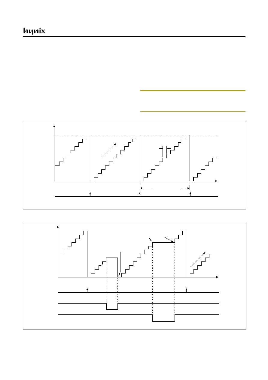
GMS81C5108
JUNE 2001 Ver 1.0
49
These timers have each 8-bit count register and data regis-
ter. The count register is increased by every internal or ex-
ternal clock input. The internal clock has a prescaler divide
ratio option of 2, 4, 8, 32,128, 512, 1024 (selected by con-
trol bits T0CK2, T0CK1 and T0CK0 of register TM0) and
1, 2, 8 (selected by control bits T1CK1 and T1CK0 of reg-
ister TM1).
In the Timer, timer register T
X
increases from 00
H
until it
matches TDR
X
and then reset to 00
H
. If the value of T
X
is
equal with TDR
X
, Timer
X
interrupt is occurred (latched in
T
X
IF bit). TDR0 and T0 register are in same address, so
this register is read from T0 and written to TDR0.
In counter function, the counter is increased every 0-to 1
(rising edge) transition of EC0 pin. In order to use counter
function, the bit R03 of the R0 Direction Register (R0DR)
should be set to "0" and the bit EC0 of Port Mode Register
(PMR) should set to "1". The Timer 0 can be used as a
counter by pin EC0 input, but Timer 1 can not used as a
counter.
Note: The contents of TDR0 and TDR1 must be initialized
(by software) with the value between 1
H
and 0FF
H
,
not 0
H
.
Figure 12-4 Counting Example of Timer Data Registers
Figure 12-5 Timer Count Operation
~~
Timer 0 (T0IF)
Interrupt
TDR0
TIME
Occur interrupt
Occur interrupt
Occur interrupt
Interrupt period
up
-c
ou
nt
~~
~~
0
1
2
3
4
5
6
7
8
9
n
n-1
P
CP
= P
CP
x (n+1)
Timer 0 (T0IF)
Interrupt
TDR0
TIME
Occur interrupt
Occur interrupt
stop
clear & start
disable
enable
Start & Stop
T0ST
T0CN
Control count
up
-c
ou
nt
~~
~~
T0ST = 0
T0ST = 1
T0CN = 0
T0CN = 1
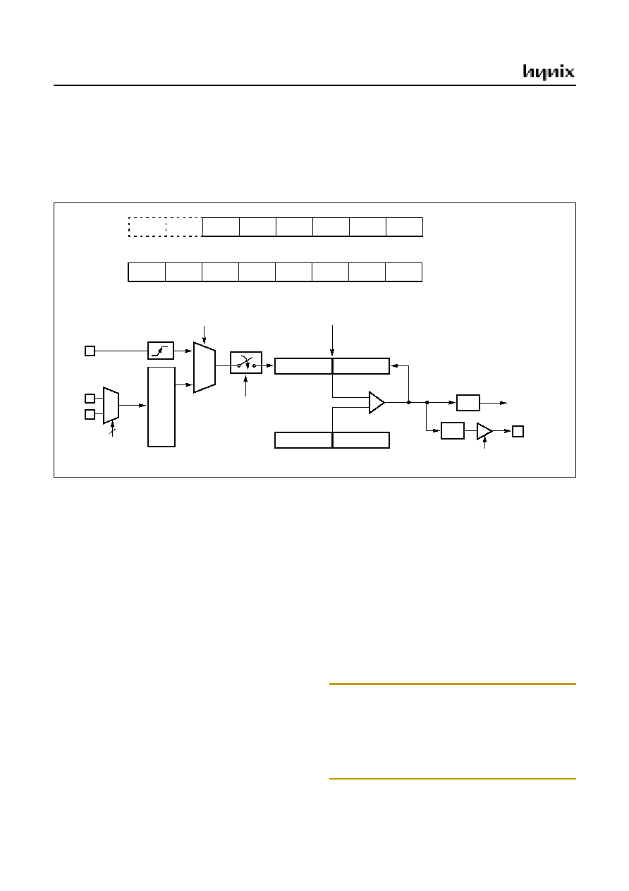
GMS81C5108
50
JUNE 2001 Ver 1.0
12.2 16 Bit Timer/Counter Mode
The Timer register is running with 16 bits. A 16-bit timer/
counter register T0, T1 are increased from 0000
H
until it
matches TDR0, TDR1 and then resets to 0000
H
. The
match output generates Timer 0 interrupt not Timer 1 in-
terrupt.
The clock source of the Timer 0 is selected either internal
or external clock by bit T0CK2, T0CK1 and T0CK0.
In 16-bit mode, the bits T1CK1,T1CK0 and 16BIT of TM1
should be set to "1" respectively.
Figure 12-6 16-bit Timer / Counter Mode
12.3 8-Bit Capture Mode
The Timer 0 capture mode is set by bit CAP0 of timer
mode register TM0 (bit CAP1 of timer mode register TM1
for Timer 1) as shown in Figure 12-7.
As mentioned above, not only Timer 0 but Timer 1 can also
be used as a capture mode.
The Timer/Counter register is increased in response inter-
nal or external input. This counting function is same with
normal timer mode, and Timer interrupt is generated when
timer register T0 (T1) increases and matches TDR0
(TDR1).
This timer interrupt in capture mode is very useful when
the pulse width of captured signal is more wider than the
maximum period of Timer.
For example, in Figure 12-9, the pulse width of captured
signal is wider than the timer data value (FF
H
) over 2
times. When external interrupt is occurred, the captured
value (13
H
) is more little than wanted value. It can be ob-
tained correct value by counting the number of timer over-
flow occurrence.
Timer/Counter still does the above, but with the added fea-
ture that a edge transition at external input INTx pin causes
the current value in the Timer x register (T0,T1), to be cap-
tured into registers CDRx (CDR0, CDR1), respectively.
After captured, Timer x register is cleared and restarts by
hardware.
It has three transition modes: "falling edge", "rising edge",
"both edge" which are selected by interrupt edge selection
register IESR (Refer to External interrupt section). In addi-
tion, the transition at INTx pin generate an interrupt.
Note: The CDR0, TDR0 and T0 are in same address. In
the capture mode, reading operation is read the
CDR0 and in timer mode, reading operation is read
the T0. TDR0 is only for writing operation.
The CDR1, T1 are in same address, the TDR1 is lo-
cated in different address. In the capture mode,
reading operation is read the CDR1
TM0
ADDRESS : 0E0
H
RESET VALUE : --000000
B
-
-
CAP0
T0CK2
T0CK1
T0CK0
T0CN
T0ST
TM1
ADDRESS : 0E2
H
RESET VALUE : 00000000
B
POL
16BIT
PWME
CAP1
T1CK1
T1CK0
T1CN
T1ST
0
X
X
X
X
X
X
1
0
0
1
1
X
X
÷
2
÷
4
÷
128
÷
512
÷
8
÷
32
EC0
Edge Detector
MUX
1
T1 (8-bit)
TDR1 (8-bit)
T0IF
CLEAR
COMPARATOR
TIMER 0
INTERRUPT
T 0 (8 -b it)
TDR0 (8-bit)
T0ST
0 : Stop
1 : Clear and Start
T0CN
T0CK[2:0]
F/F
COMPO (R31)
÷
1024
X : The value "0" or "1" corresponding your operation.
SX
IN
0X
1X
X
IN
SCMR[1:0]
2
PWMO
[PMR.6]
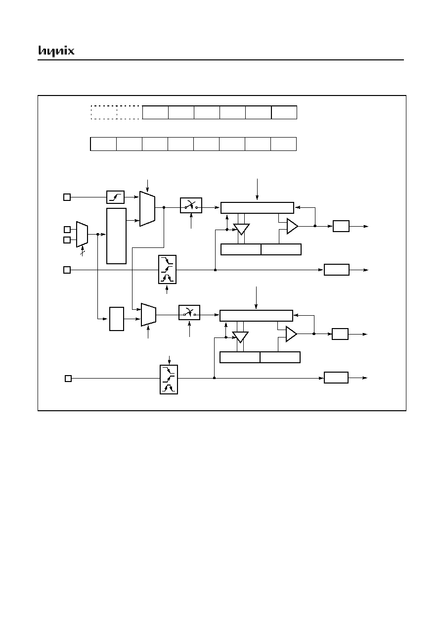
GMS81C5108
JUNE 2001 Ver 1.0
51
Figure 12-7 8-bit Capture Mode
÷
1
÷
2
÷
8
TM0
ADDRESS : 0E0H
RESET VALUE : --000000
B
-
-
CAP0
T0CK2
T0CK1
T0CK0
T0CN
T0ST
TM1
ADDRESS : 0E2H
RESET VALUE : 00000000
B
POL
16BIT
PWME
CAP1
T1CK1
T1CK0
T1CN
T1ST
1
X
X
X
X
X
X
0
0
1
X
X
X
X
÷
2
÷
4
÷
128
÷
512
÷
8
÷
32
EC0
Edge Detector
MUX
MUX
1
1
T0 (8-bit)
CDR0 (8-bit)
T0IF
CLEAR
COMPARATOR
TIMER 0
INTERRUPT
T0ST
0 : Stop
1 : Clear and Start
T0CN
T1CN
T0CK[2:0]
T1CK[1:0]
TDR0 (8-bit)
INT0IF
INT 0
INTERRUPT
INT0
T1 (8-bit)
CDR1 (8-bit)
T1IF
CLEAR
COMPARATOR
TIMER 1
INTERRUPT
TDR1 (8-bit)
INT1IF
INT 1
INTERRUPT
INT1
T0ST
0 : Stop
1 : Clear and Start
IESR[1:0]
IESR[3:2]
CAPTURE
CAPTURE
÷
1024
SX
IN
0X
1X
X
IN
SCMR[1:0]
2
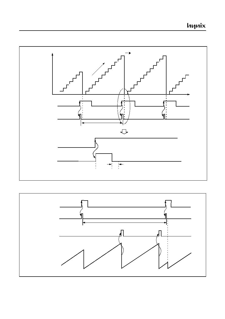
GMS81C5108
52
JUNE 2001 Ver 1.0
Figure 12-8 Input Capture Operation
Figure 12-9 Excess Timer Overflow in Capture Mode
~~
Ext. INT0 Pin
Interrupt Request
T0
TIME
up
-co
un
t
~~
~~
0
1
2
3
4
5
6
7
8
9
n
n-1
Capture
(Timer Stop)
Clear & Start
Interrupt Interval Period
Delay
(INT0IF)
Ext. INT0 Pin
Interrupt Request
(INT0IF)
This value is loaded to CDR0
Interrupt Interval Period = FF
H
+ 01
H
+ FF
H
+01
H
+ 13
H
= 213
H
FF
H
FF
H
Ext. INT0 Pin
Interrupt Request
(INT0IF)
00
H
00
H
Interrupt Request
(T0IF)
T0
13
H
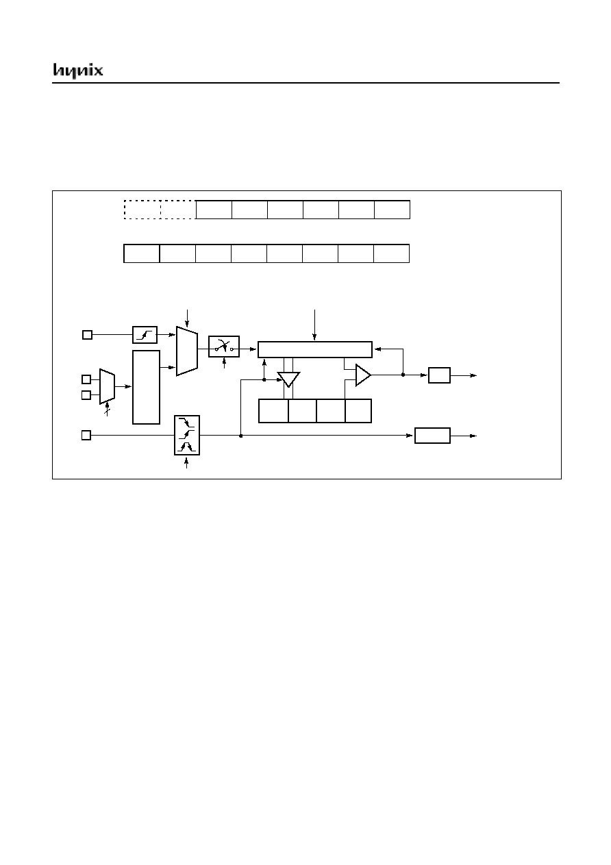
GMS81C5108
JUNE 2001 Ver 1.0
53
12.4 16-bit Capture Mode
16-bit capture mode is the same as 8-bit capture, except
that the Timer register is running with 16 bits.
The clock source of the Timer 0 is selected either internal
or external clock by bit T0CK2, T0CK1 and T0CK0.
In 16-bit mode, the bits T1CK1,T1CK0 and 16BIT of TM1
should be set to "1" respectively.
Figure 12-10 16-bit Capture Mode
12.5 8-Bit (16-Bit) Compare OutPut Mode
The GMS81C5108 has a function of Timer Compare Out-
put. To pulse out, the timer match can goes to port pin
(R31) as shown in Figure 12-3 and Figure 12-6. Thus,
pulse out is generated by the timer match. These operation
is implemented to pin, R31/PWM.
In this mode, the bit PWMO of Port Mode Register (PMR)
should be set to "1", and the bit PWME of Timer1 Mode
Register (TM1) should be cleared to "0".
In addition, 16-bit Compare output mode is available, also.
This pin output the signal having a 50 : 50 duty square
wave, and output frequency is same as below equation.
12.6 PWM Mode
The GMS81C5108 has one high speed PWM (Pulse Width
Modulation) function which shared with Timer1.
In PWM mode, the R31/PWM pin operates as a 10-bit res-
olution PWM output port. For this mode, the bit PWM of
Port Mode Register (PMR) and the bit PWME of timer1
mode register (TM1) should be set to "1" respectively.
The period of the PWM output is determined by the
T1PPR (PWM Period Register) and PWMHR[3:2] (bit3,2
of PWM High Register) and the duty of the PWM output
is determined by the T1PDR (PWM Duty Register) and
PWMHR[1:0] (bit1,0 of PWM High Register).
The user can use PWM data by writing the lower 8-bit pe-
riod value to the T1PPR and the higher 2-bit period value
to the PWMHR[3:2]. And the duty value can be used with
the T1PDR and the PWMHR[1:0] in the same way.
The T1PDR is configured as a double buffering for glitch-
TM0
ADDRESS : 0E0H
RESET VALUE : --000000
B
-
-
CAP0
T0CK2
T0CK1
T0CK0
T0CN
T0ST
TM1
ADDRESS : 0E2H
RESET VALUE : 00000000
B
POL
16BIT
PWME
CAP1
T1CK1
T1CK0
T1CN
T1ST
1
X
X
X
X
X
X
1
0
X
1
1
X
X
÷
2
÷
4
÷
128
÷
512
÷
8
÷
32
EC0
Edge Detector
MUX
1
T0 + T1 (16-bit)
TDR1
T0IF
CLEAR
COMPARATOR
TIMER 0
INTERRUPT
T0ST
0 : Stop
1 : Clear and Start
T0CN
T0CK[2:0]
TDR0
INT0IF
INT 0
INTERRUPT
INT0
IESR[1:0]
CAPTURE
CDR1
CDR0
(8-bit)
(8-bit)
(8-bit)
(8-bit)
÷
1024
X : The value "0" or "1" corresponding your operation.
SX
IN
0X
1X
X
IN
SCMR[1:0]
2
f
COMP
Oscillation Frequency
2
Prescaler Value
TDR
1
)
+
(
×
×
--------------------------------------------------------------------------------------
=
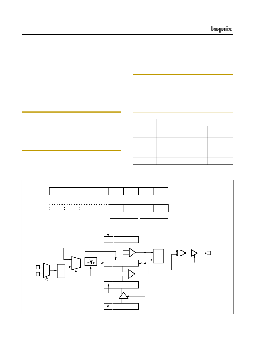
GMS81C5108
54
JUNE 2001 Ver 1.0
less PWM output. In Figure 12-11, the duty data is trans-
ferred from the master to the slave when the period data
matched to the counted value. (i.e. at the beginning of next
duty cycle).
The bit POL0 of TM1 decides the polarity of duty cycle.
The duty value can be changed when the PWM outputs.
However the changed duty value is output after the current
period is over. And it can be maintained the duty value at
present output when changed only period value shown as
Figure 12-13. As it were, the absolute duty time is not
changed in varying frequency.
Note: If the user need to change mode from the Timer1
mode to the PWM mode, the Timer1 should be
stopped firstly, and then set period and duty register
value. If user writes register values and changes
mode to PWM mode while Timer1 is in operation,
the PWM data would be different from expected
data in the beginning.
The relation of frequency and resolution is in inverse pro-
portion. Table 12-2 shows the relation of PWM frequency
vs. resolution.
PWM Period = [PWMHR[3:2]T1PPR+1] X Source Clock
PWM Duty = [PWMHR[1:0]T1PDR+1] X Source Clock
If it needed more higher frequency of PWM, it should be
reduced resolution.
Note: If the duty value and the period value are same, the
PWM output is determined by the bit POL0 (1: High,
0: Low). And if the duty value is set to "00
H
"
, the
PWM output is determined by the bit POL0(1: Low,
0: High). The period value must be same or more
than the duty value, and 00
H
cannot be used as the
period value.
Table 12-2 PWM Frequency vs. Resolution at 4MHz
Figure 12-11 PWM Mode
Resolution
Frequency
T1CK[1:0]
=00 (250nS)
T1CK[1:0]
=01 (500nS)
T1CK[1:0]
=10 (2uS)
10-bit
3.9KHz
1.95KHz
0.49KHZ
9-bit
7.8KHz
3.9KHz
0.98KHZ
8-bit
15.6KHz
7.8KHz
1.95KHz
7-bit
31.25KHz
15.6KHz
3.90KHz
÷
1
÷
2
÷
8
PWMHR
ADDRESS : 0E5
H
RESET VALUE : ----0000
B
-
-
-
-
PWM03
PWM02
PWM01
PWM00
X
X
X
X
MUX
1
T1CN
T1CK[1:0]
T1 (8-bit)
T1ST
0 : Stop
1 : Clear and Start
CLEAR
COMPARATOR
COMPARATOR
T1PDR (8-bit)
PWMHR[1:0]
T1PPR (8-bit)
PWMHR[3:2]
T1PDR (8-bit)
S
Q
R
POL
PWMO
R31/PWM
T0 clock source
TM1
ADDRESS : 0E2
H
RESET VALUE : 00
H
POL
16BIT
PWME
CAP1
T1CK1
T1CK0
T1CN
T1ST
X
0
1
0
X
X
X
X
[PMR.6]
Period High
Duty High
Slave
Master
Bit Manipulation Not Available
X : The value "0" or "1" corresponding your operation.
SX
IN
0X
1X
X
IN
SCMR[1:0]
2
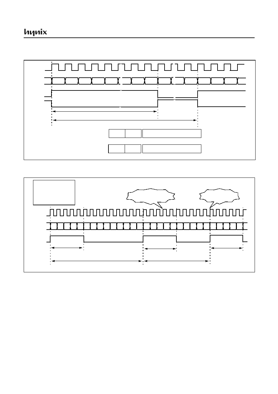
GMS81C5108
JUNE 2001 Ver 1.0
55
Figure 12-12 Example of PWM at 4MHz
Figure 12-13 Example of Changing the Period in Absolute Duty Cycle (@4MHz)
Example:
Timer1 @4Mhz,
4kHz -
20
%
duty PWM mode
LDM R3DR,#0000_XX1XB ;R31 output
LDM TM1,#0010_0000B ;pwm enable
LDM T1PWHR,#0000_1100B ;20% duty
LDM T1PPR,#1110_0111B ;period 250uS
LDM T1PDR,#1100_0111B ;duty 50uS
LDM RSR,#X1XX_XXXXB ;set pwm port.
LDM TM1,#0010_0011B ;timer1 start
X means don't care
fxin
T1
PWM
~~
~~
~~
01
02
03
04
7F
80
81
3FF
01
02
~~
~~
~~
~~
~~
~~
~~
POL=1
PWM
POL=0
Duty Cycle [80
H
+1 x 250nS = 32.25uS]
Period Cycle [3FF
H
x 250nS = 256uS, 3.9kHz]
PWMHR = 0C
H
T1PPR = FF
H
T1PDR = 80
H
T1CK[1:0] = 00 (250nS)
PWM03
PWM02
PWM01
PWM00
T1PPR (8-bit)
T1PDR (8-bit)
Period
Duty
1
1
FF
H
0
0
80
H
00
00
Source
T1
PWM
POL=1
Duty Cycle
Period Cycle [0D
H
+1 x 2uS = 28uS, 35.7kHz]
P W M H R = 0 0
H
T 1P P R = 0 D
H
T 1P D R = 0 4
H
T 1C K [1 :0 ] = 1 0 (2 uS )
00 01
02
03
04
05
07
08
0A 0B 0C 0D 00 01 02
03
04
05 06
07
08
09
00
01
02 03
06
09
04
[04
H
+1 x 2uS = 10uS]
Duty Cycle
[04
H
+1 x 2uS = 10uS]
Period Cycle [09
H
+1 x 2uS = 20uS, 50kHz]
Duty Cycle
[04
H
+1 x 2uS = 10uS]
Write T1PPR to 09
H
Period changed
clock
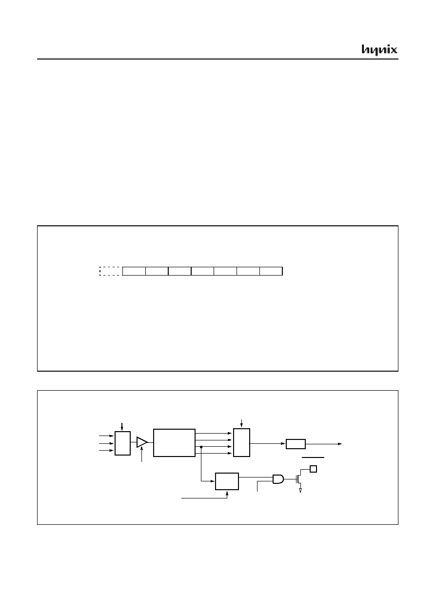
GMS81C5108
56
JUNE 2001 Ver 1.0
13. Watch Timer/Watch Dog Timer
This has two functions, one is the interrupt occurrence for
watch time and the other is the signal generation of
WDTOUTB for watch dog.
13.1 Watch Timer
The watch timer consists of the clock selector, 21-bit bina-
ry counter and watch timer mode register. It is a multi-pur-
pose timer. It is generally used for watch design.
The bit 1,2 of WTMR select the clock source of watch tim-
er among sub-clock,
f
MAIN
÷
2
7
of main-clock and
f
MAIN
of
main-clock. The
f
MAIN
of main-clock is used usually for
watch timer test, so generally it is not used for the clock
source of watch timer. The
f
MAIN
÷
2
7
of main-clock is used
when the single clock system is organized. In
f
MAIN
÷
2
7
clock source, if the CPU enters into stop mode, the main-
clock is stopped and then watch timer is also stopped. If the
sub-clock is the source clock, the watch timer count cannot
be stopped. Therefore, the sub-clock does not stop but con-
tinues to oscillate even when the CPU is in the STOP
mode. The timer counter consists of 21-bit binary counter
and it can count to max 64 seconds at sub-clock.
The bit 2, 3 of WTMR select the interrupt request interval
of watch timer among 2Hz, 4Hz, 16Hz and 1/64Hz.
Figure 13-1 Watch Timer Mode Register
Figure 13-2 Watch Timer Block Diagram
WDTCL
Bit : 7 6 5 4 3 2 1 0
WDTEN
WTIN[1:0] (Watch Timer Interrupt Interval Selection)
00: 16Hz
01: 4Hz
10: 2Hz
11: 1/64Hz
WDTEN (Watch Dog Timer Enable Bit)
0: Watch Dog Timer Disable
1: Watch Dog Timer Enable
INITIAL VALUE:-0000000
B
ADDRESS: 0EF
H
WTMR (Watch Timer Mode Register)
R/W
R/W
R/W
R/W
WTCK1
WTCK0
WTIN1
WTIN0
R/W
R/W
WTEN (Watch Timer Enable Bit)
0: Watch Timer Disable
1: Watch Timer Enable
-
WTEN
R/W
WTCK[1:0] (Watch Timer Clock Source Selection)
00: Sub. Clock (f
SUB
)
WDTCL (Watch Dog Timer Clear Bit)
0: Timer running
1: WDT Clear (Auto reset after 1 cycle)
01: Main Clock (f
MAIN
÷
2
7
)
10: Main Clock (f
MAIN
)
11: -
* When f
SUB
= 32.768 kHz and f
MAIN
= 4.19 MHz
MUX
f
SUB
WDTCL
f
MAIN
21 BIT
2 Bit
16 Hz
Watch Timer
f
MAIN
÷
÷
÷
÷
2
7
WTCK[1:0]
Binary Counter
4 Hz
2 Hz
1/64 Hz
MUX
WTIN[1:0]
WTEN
WTIF
Interrupt
F/F
WDTEN
WDTOUT
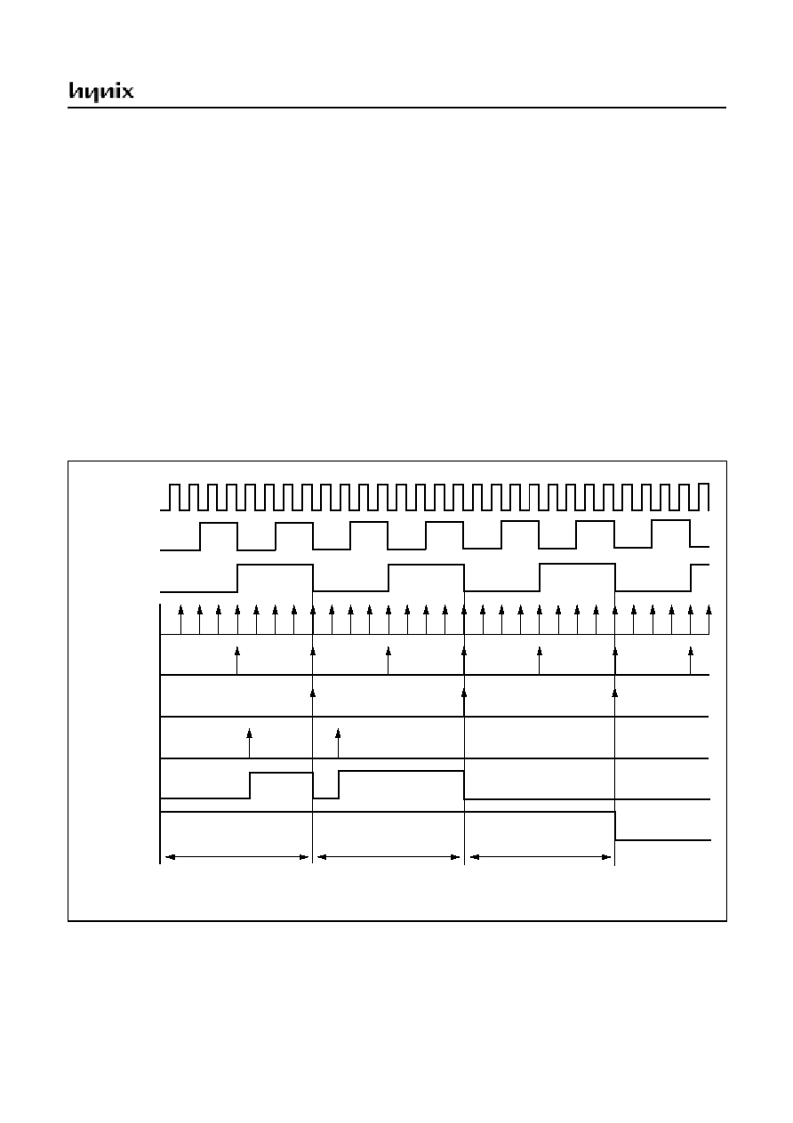
GMS81C5108
JUNE 2001 Ver 1.0
57
13.2 Watch Dog Timer
The watch dog timer (WDT) function is used for checking
program malfunction. If the watch dog timer is not reset in
a fixed time, the WDTOUTB pin outputs a low signal.
Therefore, by connecting the WDTOUTB pin and the reset
pin externally, the MCU can be reset when the malfunction
is occurred.
Usually the stop mode is used to reduce the power con-
sumption. When the stop mode is released by watch timer
interrupt, it is recommend to set the WDTCL to clear the
2-Bit counter and enter the stop mode. If the clock source
is 1/64Hz, the WDTCL cannot be cleared in 500ms. In this
case, the user should disable the WDT by clearing the
WDTEN or disconnect the WDTOUTB pin and reset pin.
Usage of Watch Timer in STOP Mode
When the system is off and the watch should be kept work-
ing, follow the steps below.
1. Determines which mode is to be performed between
main mode and sub mode when the MCU is released
from Stop mode and set the clock source of watch timer
to sub-clock.
2. Enters in STOP mode.
3. After released by watch timer interrupt, counts up timer
and refreshes LCD Display. When the performing count
up and refresh the LCD, the CPU operates either in main
frequency mode or sub frequency mode.
4. Enters in STOP mode again.
5. Repeats 3 and 4.
When using STOP mode, if the watch timer interrupt inter-
val is selected to 2Hz, the power consumption can be
reduced considerably.
fW/211 (16Hz)
INTWT (16Hz)
500msec
WDTCL
500msec
If the WDTCL is not cleared
during this interval, the WDTOUTB
will be low during next interval.
The WDTCL should
be set during this interval.
The WDTCL should
be set during this interval.
fW/213 (4Hz)
fW/214 (2Hz)
INTWT (4Hz)
INTWT (2Hz)
WDT Reset
Signal
WDTOUTB
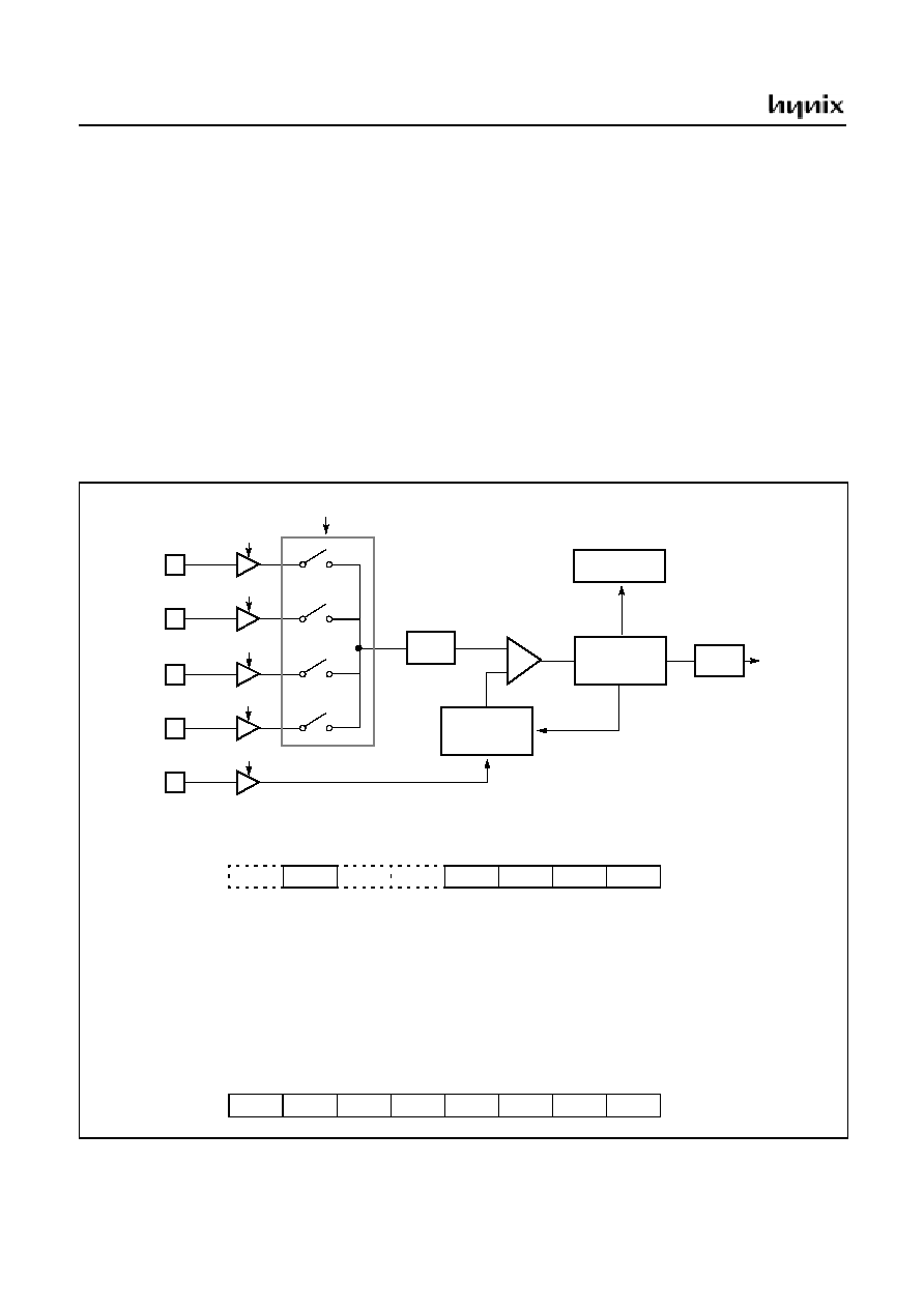
GMS81C5108
58
JUNE 2001 Ver 1.0
14. ANALOG TO DIGITAL CONVERTER
The analog-to-digital converter (A/D) allows conversion
of an analog input signal to a corresponding 8-bit digital
value. The A/D module has four analog inputs, which are
multiplexed into one sample and hold. The output of the
sample and hold is the input into the converter, which gen-
erates the result via successive approximation. The analog
supply voltage is connected to AV
DD
of ladder resistance
of A/D module.
The A/D module has two registers which are the A/D mode
register (ADMR) and A/D data register (ADDR). The
ADMR register, shown in Figure 14-1, controls the opera-
tion of the A/D converter module. The port pins can be
configured as analog inputs or digital I/O. To use analog
inputs, each port should be assigned analog input port by
setting input mode by R2DR direction register. And select
the corresponding channel to be converted by setting
ADAN[1:0].
The processing of conversion is start when the start bit
ADST is set to "1". After one cycle, it is cleared by hard-
ware. The register ADDR contains the result of the A/D
conversion. When the conversion is completed, the result
is loaded into the ADDR, the A/D conversion status bit
ADF is set to "1", and the A/D interrupt flag ADIF is set.
The block diagram of the A/D module is shown in Figure
14-1. The A/D status bit ADF is automatically set when A/
D conversion is completed, cleared when A/D conversion
is in process. The conversion time takes maximum 30 uS
(at f
MAIN
= 4MHz).
Figure 14-1 A/D Converter Block Diagram & Registers
AV
DD
R20/AN0
R21/AN1
R22/AN2
R23/AN3
ANEN
00
01
10
11
S/H
Successive
Approximation
Circuit
A D IF
Resistor
Ladder
Circuit
ADAN[1:0]
ADDR (8-bit)
Sample & Hold
A/D Interrupt
ADDRESS : 0ED
H
RESET VALUE : Undefined
A/D Converter
Data Register
ANEN
ANEN
ANEN
ANEN
ADMR (A/D Mode Register)
ADDRESS : 0EC
H
RESET VALUE : -0--0001
B
-
ADEN
-
-
ADAN1
ADAN0
ADST
ADF
ADF (A/D Status bit)
0 : A/D Conversion is in process
1 : A/D Conversion is completed
ADST (A/D Start bit)
1 : A/D Conversion is started
After 1 cycle, cleared to "0"
0 : Bit force to zero
00 : Channel 0 (R20/AN0)
01 : Channel 1 (R21/AN1)
10 : Channel 2 (R22/AN2)
11 : Channel 3 (R23/AN3)
ADEN (A/D Converter Enable bit)
1 : Enable
0 : Disable
ADDR (A/D Data Register)
ADDRESS : 0ED
H
RESET VALUE : Undefined
ADD7
ADD6
ADD5
ADD4
ADD3
ADD2
ADD1
ADD0
ADAN[1:0] (A/D Converter Input Selection)
Bit : 7 6 5 4 3 2 1 0
R/W
R/W
R/W
R
R/W
Bit : 7 6 5 4 3 2 1 0
R
R
R
R
R
R
R
R
Comparator
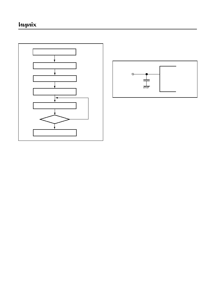
GMS81C5108
JUNE 2001 Ver 1.0
59
Figure 14-2 A/D Converter Operation Flow
A/D Converter Cautions
(1) Input range of AN0 to AN3
The input voltages of AN0 to AN3 should be within the
specification range. In particular, if a voltage above AV
DD
or below V
SS
is input (even if within the absolute maxi-
mum rating range), the conversion value for that channel
can not be indeterminated. The conversion values of the
other channels may also be affected.
(2) Noise countermeasures
In order to maintain 8-bit resolution, attention must be paid
to noise on pins AV
DD
and AN0 to AN3. Since the effect
increases in proportion to the output impedance of the an-
alog input source, it is recommended that a capacitor is
connected externally as shown below in order to reduce
noise
.
Figure 14-3 Analog Input Pin Connecting Capacitor
(3) Pins AN0/R20 to AN3/R23
The analog input pins AN0 to AN3 also function as input/
output port (PORT R2) pins. When A/D conversion is per-
formed with any of pins AN0 to AN3 selected, be sure not
to execute a PORT input instruction while conversion is in
progress, as this may reduce the conversion resolution.
Also, if digital pulses are applied to a pin adjacent to the
pin in the process of A/D conversion, the expected A/D
conversion value may not be obtainable due to coupling
noise. Therefore, avoid applying pulses to pins adjacent to
the pin undergoing A/D conversion.
(4) AV
DD
pin input impedance
A series resistor string of approximately 10K
is connect-
ed between the AV
DD
pin and the V
SS
pin.
Therefore, if the output impedance of the reference voltage
source is high, this will result in parallel connection to the
series resistor string between the AV
DD
pin and the V
SS
pin, and there will be a large reference voltage error.
ENABLE A/D CONVERTER
A/D START (ADST = 1)
NOP
ADF = 1
A/D INPUT CHANNEL SELECT
READ ADDR
YES
NO
ANALOG REFERENCE SELECT
AN0~AN3
100~1000pF
Analog
Input
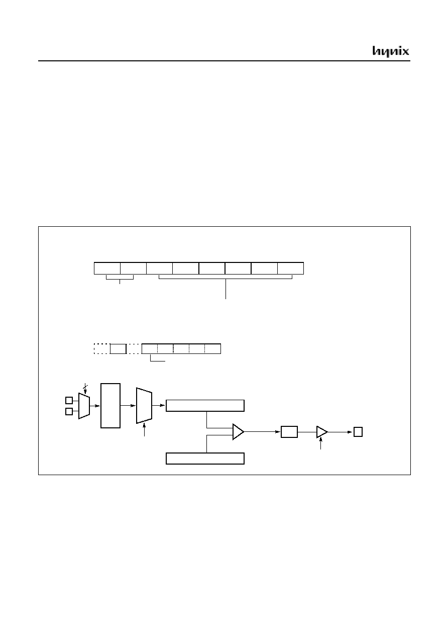
GMS81C5108
60
JUNE 2001 Ver 1.0
15. Buzzer Output Function
The buzzer driver consists of 6-bit binary counter, the
buzzer data register BDR and the clock selector. It gener-
ates square-wave which is very wide range frequency (500
Hz~125 KHz at f
MAIN
= 4MHz) by user programmable
counter.
Pin R04 is assigned for output port of Buzzer driver by set-
ting the bit BUZ of Port Mode Register (PMR) to "1".
The 6-bit buzzer counter is cleared and start the counting
by writing signal to the register BDR. It is increased from
00
H
until it matches with BDR[5:0].
Also, it is cleared by counter overflow and count up to out-
put the square wave pulse of duty 50%.
The bit 0 to 5 of BDR determines output frequency for
buzzer driving. BCD is undefined after reset, so it must be
initialized to between 0
H
and 3F
H
by software. Note that
BDR is a write-only register. Frequency calculation is fol-
lowing as shown below.
The bits BCK1, BCK0 of BDR select the source clock
from prescaler output
f
BUZ
: BUZ pin frequency
Prescaler ratio: Prescaler divide ratio by BDR[7:6]
BCD value: 6-bit compare data, BCD[5:0].
Figure 15-1 Buzzer Driver
Example: 2.5kHz output at 4MHz.
LDM
R0DR,#XXX1_XXXXB
LDM
BDR,#1001_1000B
LDM
PMR,#XXX1_XXXXB ;Buzzer ON
X means don't care
f
BUZ
Hz
(
)
Oscillator Frequency
2
Prescaler Ratio
BCD
1
+
(
)
×
×
-------------------------------------------------------------------------------
=
BDR (Buzzer Data Register)
ADDRESS : 0FD
H
RESET VALUE : 00
H
BCK1
BCK0
BCD5
BCD4
BCD3
BCD2
BCD1
BCD0
÷
64
÷
16
÷
32
MUX
COUNTER (6-bit)
BCD (6-bit)
F/F
COMPARATOR
BCK[1:0]
R04/BUZ PIN
÷
8
BCK[1:0] (Buzzer Clock Source)
BCD[5:0] (Buzzer Control Data)
BUZ
[PMR.4]
Bit manipulation is not available.
Buzzer Period Data
Bit : 7 6 5 4 3 2 1 0
W
W
W
W
W
W
W
W
SX
IN
0X
1X
X
IN
SCMR[1:0]
2
PMR (Port Mode Register)
ADDRESS :0D9
H
RESET VALUE : -0-00000
B
-
PWMO
-
BUZ
EC0
INT2
INT1
INT0
BUZ (Buzzer Output)
0: R04 Port (turn off buzzer)
1: BUZ port (turn on buzzer)
00: f
MAIN
÷
2
3
01: f
MAIN
÷
2
4
10: f
MAIN
÷
2
5
11: f
MAIN
÷
2
6
or f
SUB
÷
2
4
or f
SUB
÷
2
3
or f
SUB
÷
2
6
or f
SUB
÷
2
5
GMS81C5108
JUNE 2001 Ver 1.0
61
Buzzer Output Frequency
When main-frequency is 4MHz, buzzer frequency is
shown as below and if sub-frequency is selected as clock
source, buzzer frequency is used after dividing by 128.
Table 15-1 Buzzer Output Frequency
BDR
[5:0]
Frequency Output (kHz)
BDR
[5:0]
Frequency Output (kHz)
00
01
10
11
00
01
10
11
00
01
02
03
04
05
06
07
250.000
125.000
83.333
62.500
50.000
41.667
35.714
31.250
125.000
62.500
41.667
31.250
25.000
20.833
17.857
15.625
62.500
31.250
20.833
15.625
12.500
10.417
8.929
7.813
31.250
15.625
10.417
7.813
6.250
5.208
4.464
3.906
20
21
22
23
24
25
26
27
7.576
7.353
7.143
6.944
6.757
6.579
6.410
6.250
3.788
3.676
3.571
3.472
3.378
3.289
3.205
3.125
1.894
1.838
1.786
1.736
1.689
1.645
1.603
1.563
0.947
0.919
0.893
0.868
0.845
0.822
0.801
0.781
08
09
0A
0B
0C
0D
0E
0F
27.778
25.000
22.727
20.833
19.231
17.857
16.667
15.625
13.889
12.500
11.364
10.417
9.615
8.929
8.333
7.813
6.944
6.250
5.682
5.208
4.808
4.464
4.167
3.906
3.472
3.125
2.841
2.604
2.404
2.232
2.083
1.953
28
29
2A
2B
2C
2D
2E
2F
6.098
5.952
5.814
5.682
5.556
5.435
5.319
5.208
3.049
2.976
2.907
2.841
2.778
2.717
2.660
2.604
1.524
1.488
1.453
1.420
1.389
1.359
1.330
1.302
0.762
0.744
0.727
0.710
0.694
0.679
0.665
0.651
10
11
12
13
14
15
16
17
14.706
13.889
13.158
12.500
11.905
11.364
10.870
10.417
7.353
6.944
6.579
6.250
5.952
5.682
5.435
5.208
3.676
3.472
3.289
3.125
2.976
2.841
2.717
2.604
1.838
1.736
1.645
1.563
1.488
1.420
1.359
1.302
30
31
32
33
34
35
36
37
5.102
5.000
4.902
4.808
4.717
4.630
4.545
4.464
2.551
2.500
2.451
2.404
2.358
2.315
2.273
2.232
1.276
1.250
1.225
1.202
1.179
1.157
1.136
1.116
0.638
0.625
0.613
0.601
0.590
0.579
0.568
0.558
18
19
1A
1B
1C
1D
1E
1F
10.000
9.615
9.259
8.929
8.621
8.333
8.065
7.813
5.000
4.808
4.630
4.464
4.310
4.167
4.032
3.906
2.500
2.404
2.315
2.232
2.155
2.083
2.016
1.953
1.250
1.202
1.157
1.116
1.078
1.042
1.008
0.977
38
39
3A
3B
3C
3D
3E
3F
4.386
4.310
4.237
4.167
4.098
4.032
3.968
3.906
2.193
2.155
2.119
2.083
2.049
2.016
1.984
1.953
1.096
1.078
1.059
1.042
1.025
1.008
0.992
0.977
0.548
0.539
0.530
0.521
0.512
0.504
0.496
0.488
GMS81C5108
62
JUNE 2001 Ver 1.0
16. Serial Communication Interface
The SCI module allows 8-bits of data to be synchronously
transmitted and received. This is useful for communication
with other peripheral of microcontroller devices.This con-
sists of serial I/O data register, serial I/O mode register,
clock selection circuit octal counter and control circuit as
shown in Figure 16-1.
Figure 16-1 SCI Registers and Block Diagram
SIOM (Seriol I/O Mode Register)
ADDRESS : 0FE
H
RESET VALUE : 00000001
B
POL
MSBS
SIO1
SIO0
SICK1
SICK0
SIOST
SIOSF
SIOD (Serial I/O Data Register)
ADDRESS : 0FF
H
RESET VALUE : Undefined
Bit : 7 6 5 4 3 2 1 0
R/W
R/W
R/W
R/W
R/W
R/W
R/W
R/W
POL (Polarity Selection)
0 : Data Transmission at falling edge
(Received data latch at rising edge)
1 : Data Transmission at rising edge
(Received data latch at falling edge)
SIO[1:0] (Serial I/O Operation Mode)
00 : Normal Port (R05, R06, R07)
01 : Transmit Mode (SCK, SO, R07)
10 : Receive Mode (SCK, R06, SI)
11 : Transmit & Receive Mode (SCK, SO, SI)
SIOST (Serial I/O Operation Start Control)
0 : SIO Operation Stop
1 : SIO Operation Start
(After one SCK clock become "0")
SICK[1:0] (Serial I/O Clock Source Selection)
00: f
MAIN
÷
4
01: f
MAIN
÷
16
10: T0O (Timer 0 Output)
11: External Clock
MSBS (MSB First Transmit and Receive Selection)
0 : LSB First
1 : MSB First
SIOSF (Serial I/O Status Flag)
0 : During SIO Operation
1 : SIO Operation Finished
Bit : 7 6 5 4 3 2 1 0
R/W
R/W
R/W
R/W
R/W
R/W
R/W
R/W
SIOD7
SIOD6
SIOD5
SIOD4
SIOD3
SIOD2
SIOD1
SIOD0
R06/SO
SCMR[1:0]
2
0X
1X
X
IN
SX
IN
Pre-
scaler
SICK[1:0]
f
MAIN
÷
2
2
or f
SUB
÷
2
2
f
MAIN
÷
2
4
or f
SUB
÷
2
4
T0OV(Timer 0 Overflow)
2
00
01
10
11
R05
SCK
POL
SIO Control Circuit
SIOST
1
SIO[1:0] = 00
SICK[1:0]
11
& SIO[1:0]
00
1
0
MSBS
R07/SI
Octal Counter
SIO
(3-Bit)
SIOIF
Interrupt
SIOD(8-Bit)
SIO[1] = 1
MSBS
0
1
SIO[0] = 1
MSB
LSB
SCK
SIOSF
SIO Data Register
Start
Complete
Clock
Shift Clock
Clear
or f
SUB
÷
4
or f
SUB
÷
16
GMS81C5108
JUNE 2001 Ver 1.0
63
To accomplish communication, typically three pins are
used:
- Serial Data In
R07/SI
- Serial Data Out
R06/SO
- Serial Clock
R05/SCK
The serial data transfer operation mode is decided by set-
ting the SIO1 and SIO0 and the transfer clock rate is decid-
ed by setting the SICK1 and SICK0 of SCI Mode Control
Register as shown in Figure 16-1. And the polarity of
transfer clock is selected by setting the POL. The MSBS
bit is used to select which bit would be sending or receiv-
ing.
16.1 Data Transmit/Receive Timing
The SCI operation is executed by setting the SIOST bit to
"1". The SIOST bit is cleared to "0" automatically after 1
machine cycle. The Serial output data is shift in or shift out
at edge decided by POL. Interrupt is occurred when the
eight in/out datas is counted by octal counter.
Figure 16-2 SCI Timing Diagram
SIO1
SIO0
Function Selection
Port Selection
R05/SCK
R06/SO
R07/SI
0
0
-
R05
R06
R07
0
1
Transmit Mode
SCK
SO
R07
1
0
Receive Mode
SCK
R06
SI
1
1
Transmit and Receive
SCK
SO
SI
D1
D2
D3
D4
D6
D7
D0
D5
D 1
D 2
D 3
D 4
D 6
D 7
D 0
D 5
SIOST
R05/SCK
(POL=1)
R05/SCK
(POL=0)
R06/SO
R07/SI
SIOIF
(SCI Int. Req)
MSBS=0
SIOSF
GMS81C5108
64
JUNE 2001 Ver 1.0
16.2 The method of Serial I/O
1. Select transmission/receiving mode
When external clock is used, the frequency should be less than
1MHz and recommended duty is 50%.
2. In case of sending mode, write data to be send to SIOD.
3. Set SIOST to "1" to start serial transmission.
If both transmission mode is selected and transmission is per-
formed simultaneously it would be made error.
4. The SIO interrupt is generated at the completion of SIO and
SIOSF is set to "1".
5. In case of receiving mode, the received data is acquired by
reading the SIOD.
Figure 16-3 SCI Timing Diagram at POL=1
D1
D2
D3
D4
D6
D7
D0
D5
D 1
D 2
D 3
D 4
D 6
D 7
D 0
D 5
SIOST
SCLK [R05]
(POL=1)
SOUT [R06]
SIN [R07]
SIOIF
SIOSF
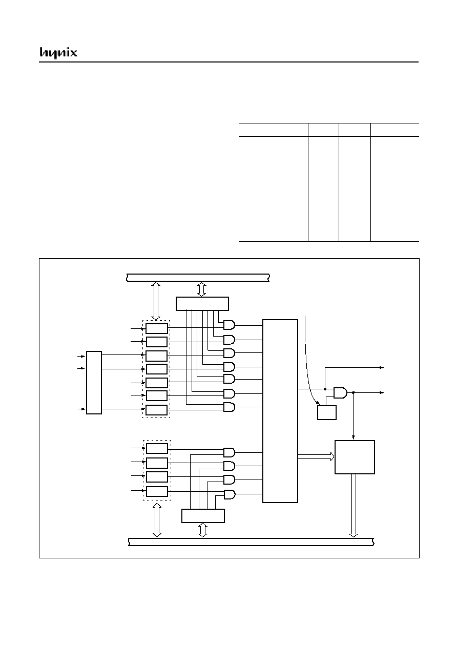
GMS81C5108
JUNE 2001 Ver 1.0
65
17. INTERRUPTS
The GMS81C5108 interrupt circuits consist of Interrupt
enable register (IENH, IENL), Interrupt request flag
(IRQH, IRQL), Interrupt Edge Selection Register (IESR),
priority circuit and Master enable flag ("I" flag of PSW).
The configuration of interrupt circuit is shown in Figure
17-1 and Interrupt priority is shown in Table 17-1 .
The flags that actually generate these interrupts are bit
INT0F, INT1F and INT2F in Register IRQH. When an ex-
ternal interrupt is generated, the flag that generated it is
cleared by the hardware when the service routine is vec-
tored to only if the interrupt was transition-activated.
The Timer 0 and Timer 2 Interrupts are generated by T0IF
and T1IF, which are set by a match in their respective tim-
er/counter register. The AD converter Interrupt is generat-
ed by ADIF which is set by finishing the analog to digital
conversion. The Basic Interval Timer Interrupt is generat-
ed by BITIF which is set by overflow of the Basic Interval
Timer Register (BITR).
Table 17-1 Interrupt Priority
Figure 17-1 Block Diagram of Interrupt Function
Reset/Interrupt
Symbol
Priority
Vector Addr.
Hardware Reset
Key Scan Interrupt
BIT Interrupt
External Interrupt 0
External Interrupt 1
Timer 0 Interrupt
Timer 1 Interrupt
External Interrupt 2
Remocon Interrupt
AD Interrupt
SIO Interrupt
Watch Timer Interrupt
RESET
KS
BIT
INT0
INT1
T0
T1
INT2
REM
AD
SIO
WT
-
1
2
3
4
5
6
7
8
9
10
11
FFFE
H
FFFC
H
FFFA
H
FFF8
H
FFF6
H
FFF4
H
FFF2
H
FFF0
H
FFEE
H
FFEC
H
FFEA
H
FFE8
H
BIT
SIOIF
ADIF
A/D Converter
Remocon
Timer 1
Timer 0
Ext. Int. 1
Ext. Int. 0
IENH
Interrupt Enable
Interrupt Enable
IRQH
IRQL
Interrupt
Vector
Address
Generator
Internal bus line
Register (Lower byte)
Internal bus line
Register (Higher byte)
Release STOP
To CPU
Interrupt Master
Enable Flag
I Flag
IENL
Pr
ior
i
t
y
Co
ntr
o
l
I-flag is in PSW, it is cleared by "DI", set by
"EI" instruction.When it goes interrupt service,
I-flag is cleared by hardware, thus any other
interrupt are inhibited. When interrupt service is
completed by "RETI" instruction, I-flag is set to
"1" by hardware.
KSIF
BITIF
INT0IF
INT1IF
REMIF
6
5
4
6
5
4
IESR
TOIF
T1IF
INT2IF
3
2
1
0
WT
WTIF
3
Key Scan
Ext. Int. 2
SIO
GMS81C5108
66
JUNE 2001 Ver 1.0
The External Interrupts INT0, INT1 and INT2 can each be
transition-activated (1-to-0, 0-to-1 and both transiton).The
interrupts are controlled by the interrupt master enable flag
I-flag (bit 2 of PSW), the interrupt enable register (IENH,
IENL) and the interrupt request flag (IRQH, IRQL) except
Power-on reset and software BRK interrupt.
Interrupt enable registers are shown in Figure 17-2. These
registers are composed of interrupt enable flags of each in-
terrupt source, these flags determine whether an interrupt
will be accepted or not. When enable flag is "0", a corre-
sponding interrupt source is prohibited. Note that PSW
contains also a master enable bit, I-flag, which disables all
interrupts at once. When an interrupt is occurred, the I-flag
is cleared and disable any further interrupt, the return ad-
dress and PSW are pushed into the stack and the PC is vec-
tored to. Once in the interrupt service routine the source(s)
of the interrupt can be determined by polling the interrupt
request flag bits.
The interrupt request flag bit(s) must be cleared by soft-
ware before re-enabling interrupts to avoid recursive inter-
rupts. The Interrupt Request flags are able to be read and
written.
Figure 17-2 Interrupt Enable Registers and Interrupt Request Registers
17.1 Interrupt Sequence
An interrupt request is held until the interrupt is accepted
or the interrupt latch is cleared to "0" by a reset or an in-
struction. Interrupt acceptance sequence requires 8 f
OSC
(2
µ
s at f
MAIN
=4MHz) after the completion of the current in-
struction execution. The interrupt service task is terminat-
ed upon execution of an interrupt return instruction
[RETI].
Interrupt acceptance
1. The interrupt master enable flag (I-flag) is cleared to
"0" to temporarily disable the acceptance of any follow-
ing maskable interrupts. When a non-maskable inter-
rupt is accepted, the acceptance of any following
interrupts is temporarily disabled.
2. Interrupt request flag for the interrupt source accepted is
cleared to "0".
3. The contents of the program counter (return address)
and the program status word are saved (pushed) onto the
stack area. The stack pointer decreases 3 times.
4. The entry address of the interrupt service program is
read from the vector table address and the entry address
is loaded to the program counter.
5. The instruction stored at the entry address of the inter-
rupt service program is executed.
IENH (Interrupt Enable High Register)
ADDRESS : 0DB
H
RESET VALUE : -0000000
B
-
KSE
BITE
INT0E
INT1E
T0E
T1E
INT2E
ADDRESS : 0DA
H
RESET VALUE : -0000---
B
-
REME
ADE
SIOE
WTE
-
-
-
IENL (Interrupt Enable Low Register)
IRQH (Interrupt Request High Register)
IRQL (Interrupt Request Low Register)
0 : Disable
1 : Enable
Enables or disables the interrupt individually
If flag is cleared, the interrupt is disabled.
0 : Not occurred
1 : Interrupt request is occurred
Shows the interrupt occurrence
Bit : 7 6 5 4 3 2 1 0
R/W
R/W
R/W
R/W
R/W
R/W
R/W
Bit : 7 6 5 4 3 2 1 0
R/W
R/W
R/W
R/W
ADDRESS : 0DD
H
RESET VALUE : -0000000
B
-
KSIF
BITIF
INT0IF
INT1IF
T0IF
T1IF
INT2IF
Bit : 7 6 5 4 3 2 1 0
R/W
R/W
R/W
R/W
R/W
R/W
R/W
ADDRESS : 0DC
H
RESET VALUE : -0000---
B
-
REMIF
ADIF
SIOIF
WTIF
-
-
-
Bit : 7 6 5 4 3 2 1 0
R/W
R/W
R/W
R/W
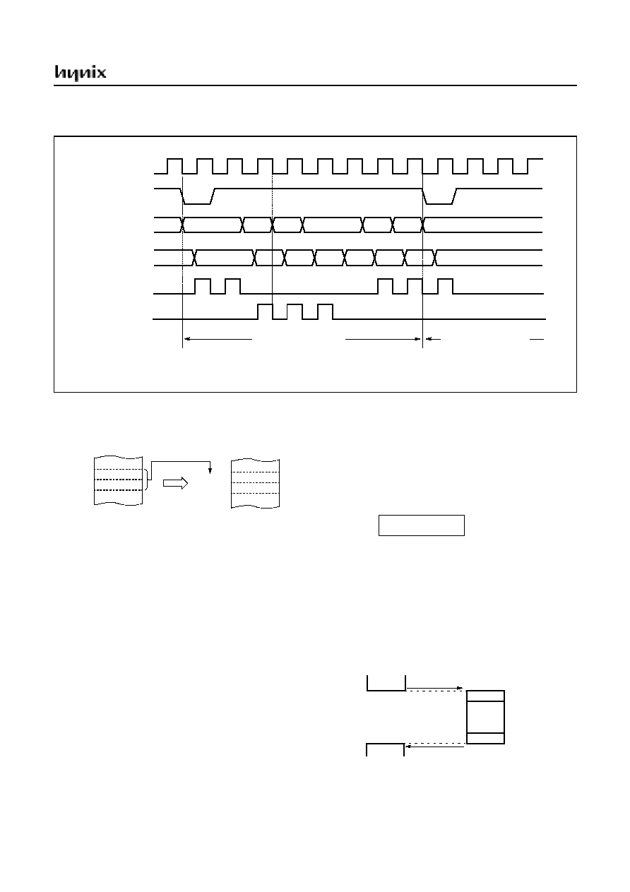
GMS81C5108
JUNE 2001 Ver 1.0
67
Figure 17-3 Timing chart of Interrupt Acceptance and Interrupt Return Instruction
An interrupt request is not accepted until the I-flag is set to
"1" even if a requested interrupt has higher priority than
that of the current interrupt being serviced.
When nested interrupt service is required, the I-flag should
be set to "1" by "EI" instruction in the interrupt service
program. In this case, acceptable interrupt sources are se-
lectively enabled by the individual interrupt enable flags.
Saving/Restoring General-purpose Register
During interrupt acceptance processing, the program
counter and the program status word are automatically
saved on the stack, but accumulator and other registers are
not saved itself. If necessary, these registers should be
saved by the software. Also, when multiple interrupt ser-
vices are nested, it is necessary to avoid using the same
data memory area for saving registers.
The following method is used to save/restore the general-
purpose registers.
Example: Register saving
General-purpose registers are saved or restored by using
push and pop instructions.
V.L.
System clock
Address Bus
PC
SP
SP-1
SP-2
V.H.
New PC
V.L.
Data Bus
Not used
PCH
PCL
PSW
ADL
OP code
ADH
Instruction Fetch
Internal Read
Internal Write
Interrupt Processing Step
Interrupt Service Routine
V.L. and V.H. are vector addresses.
ADL and ADH are start addresses of interrupt service routine as vector contents.
Basic Interval Timer
012
H
0E3
H
0FFFA
H
0FFFB
H
0E
H
2E
H
0E312
H
0E313
H
Entry Address
Correspondence between vector table address for BIT interrupt
and the entry address of the interrupt service program.
Vector Table Address
INTxx:
PUSH
A
PUSH
X
PUSH
Y
;SAVE ACC.
;SAVE X REG.
;SAVE Y REG.
interrupt processing
POP
Y
POP
X
POP
A
RETI
;RESTORE Y REG.
;RESTORE X REG.
;RESTORE ACC.
;RETURN
main routine
interrupt
service routine
saving
registers
restoring
registers
acceptance of
interrupt
interrupt return
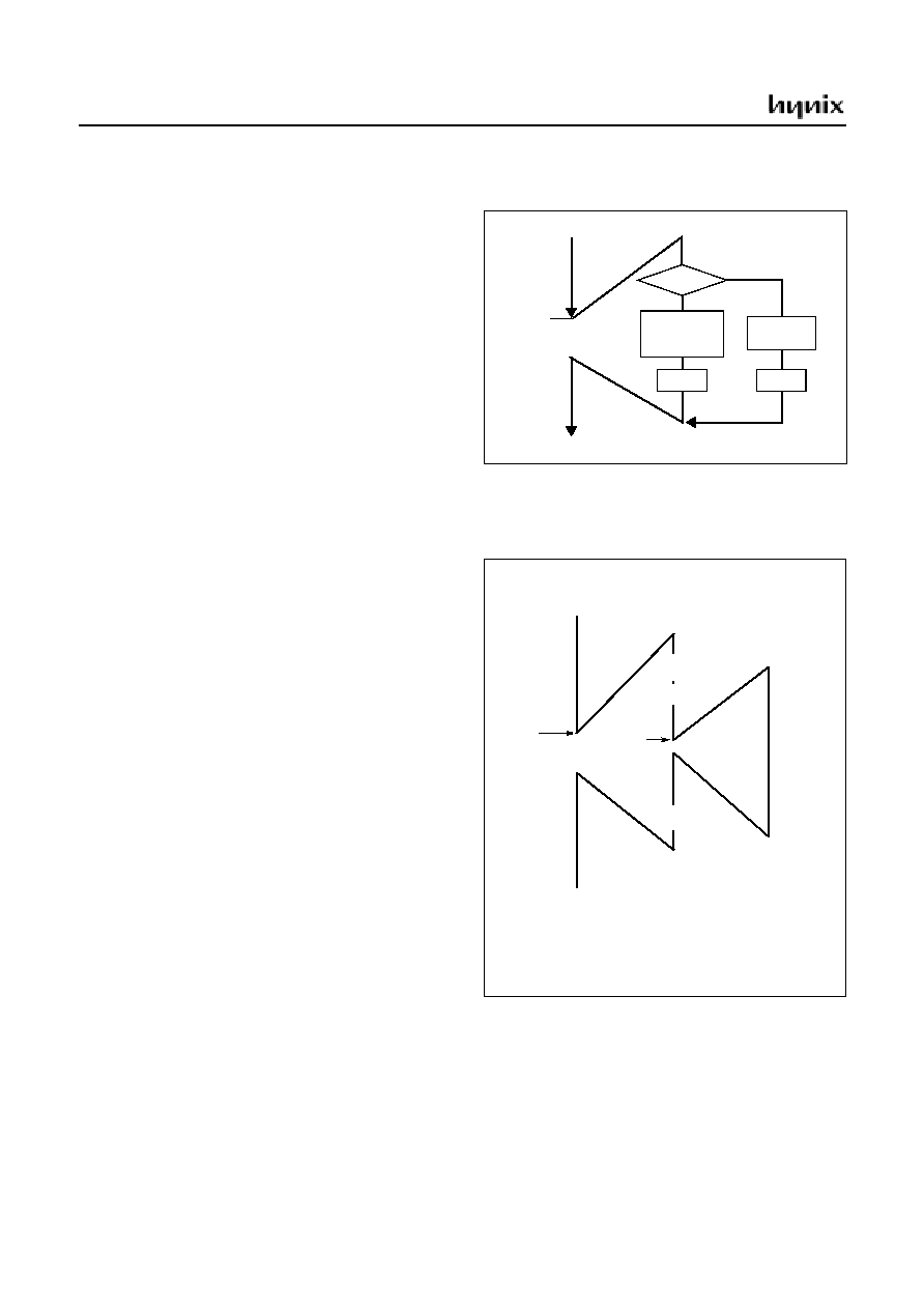
GMS81C5108
68
JUNE 2001 Ver 1.0
17.2 BRK Interrupt
Software interrupt can be invoked by BRK instruction,
which has the lowest priority order.
Interrupt vector address of BRK is shared with the vector
of TCALL 0 (Refer to Program Memory Section). When
BRK interrupt is generated, B-flag of PSW is set to distin-
guish BRK from TCALL 0.
Each processing step is determined by B-flag as shown in
Figure 17-4.
Figure 17-4 Execution of BRK/TCALL0
17.3 Multi Interrupt
If two requests of different priority levels are received si-
multaneously, the request of higher priority level is ser-
viced. If requests of the interrupt are received at the same
time simultaneously, an internal polling sequence deter-
mines by hardware which request is serviced.
However, multiple processing through software for special
features is possible. Generally when an interrupt is accept-
ed, the I-flag is cleared to disable any further interrupt. But
as user sets I-flag in interrupt routine, some further inter-
rupt can be serviced even if certain interrupt is in progress.
Example: Even though Timer1 interrupt is in progress,
INT0 interrupt serviced without any suspend.
TIMER1:
PUSH
A
PUSH
X
PUSH
Y
LDM
IENH,#80H
;
Enable INT0 only
LDM
IENL,#0
;
Disable other
EI
;
Enable Interrupt
:
:
:
:
:
:
LDM
IENH,#0FFH
;
Enable all interrupts
LDM
IENL,#0F0H
POP
Y
POP
X
POP
A
RETI
.
Figure 17-5 Execution of Multi Interrupt
B-FLAG
BRK
INTERRUPT
ROUTINE
RETI
TCALL0
ROUTINE
RET
BRK or
TCALL0
=0
=1
enable INT0
TIMER 1
service
INT0
service
Main Program
service
Occur
TIMER1 interrupt
Occur
INT0
EI
disable other
enable INT0
enable other
In this example, the INT0 interrupt can be serviced without any
pending, even TIMER1 is in progress.
Because of re-setting the interrupt enable registers IENH,IENL
and master enable "EI" in the TIMER1 routine.
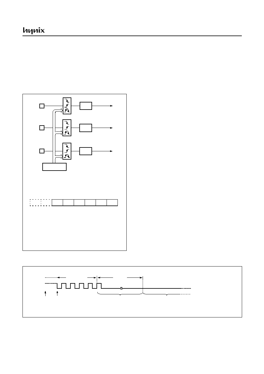
GMS81C5108
JUNE 2001 Ver 1.0
69
17.4 External Interrupt
The external interrupt on INT0, INT1 and INT2 pins are
edge triggered depending on the edge selection register
IESR (address 0D8
H
) as shown in Figure 17-6.
The edge detection of external interrupt has three transition
activated mode: rising edge, falling edge, and both edge.
Figure 17-6 External Interrupt Block Diagram
Example: To use as an INT0 and INT2
:
:
;
**** Set port as an input port R0
LDM
R0DR,#1111_1010B
;
;
**** Set port as an interrupt port
LDM
PMR,#0000_0101B
;
;
**** Set Falling-edge Detection
LDM
IESR,#0001_0001B
:
:
:
Response Time
The INT0, INT1 and INT2 edge are latched into INT0F,
INT1F and INT2F at every machine cycle. The values are
not actually polled by the circuitry until the next machine
cycle. If a request is active and conditions are right for it to
be acknowledged, a hardware subroutine call to the re-
quested service routine will be the next instruction to be
executed. The DIV itself takes twelve cycles. Thus, a max-
imum of twelve complete machine cycles elapse between
activation of an external interrupt request and the begin-
ning of execution of the first instruction of the service rou-
tine.
Interrupt response timings are shown in Figure 17-7.
Figure 17-7 Interrupt Response Timing Diagram
INT0IF
INT0
INT0 INTERRUPT
INT1IF
INT1
INT1 INTERRUPT
INT2IF
INT2
INT2 INTERRUPT
IESR
[0D8
H
]
edge
sele
c
t
ion
IESR (Ext. Interrupt Edge Selection Register)
ADDRESS : 0D8
H
RESET VALUE : --000000
B
INT21
INT2[1:0] (INT2 Edge Selections)
Bit : 7 6 5 4 3 2 1 0
R/W
R/W
R/W
R/W
R/W
R/W
INT20
INT10
INT11
INT01
INT00
00 : Int. Disable
01 : Falling (1-to-0 transition)
10 : Rising (0-to-1 transition)
11 : Both (Rising & Falling)
INT1[1:0] (INT1 Edge Selection)
00 : Int. Disable
01 : Falling (1-to-0 transition)
10 : Rising (0-to-1 transition)
11 : Both (Rising & Falling)
INT0[1:0] (INT0 Edge Selections)
00 : Int. Disable
01 : Falling (1-to-0 transition)
10 : Rising (0-to-1 transition)
11 : Both (Rising & Falling)
-
-
Interrupt Edge Selection Register)
Interrupt
goes
active
Interrupt
latched
Interrupt
processing
Interrupt
routine
8 f
OSC
max. 12 f
OSC
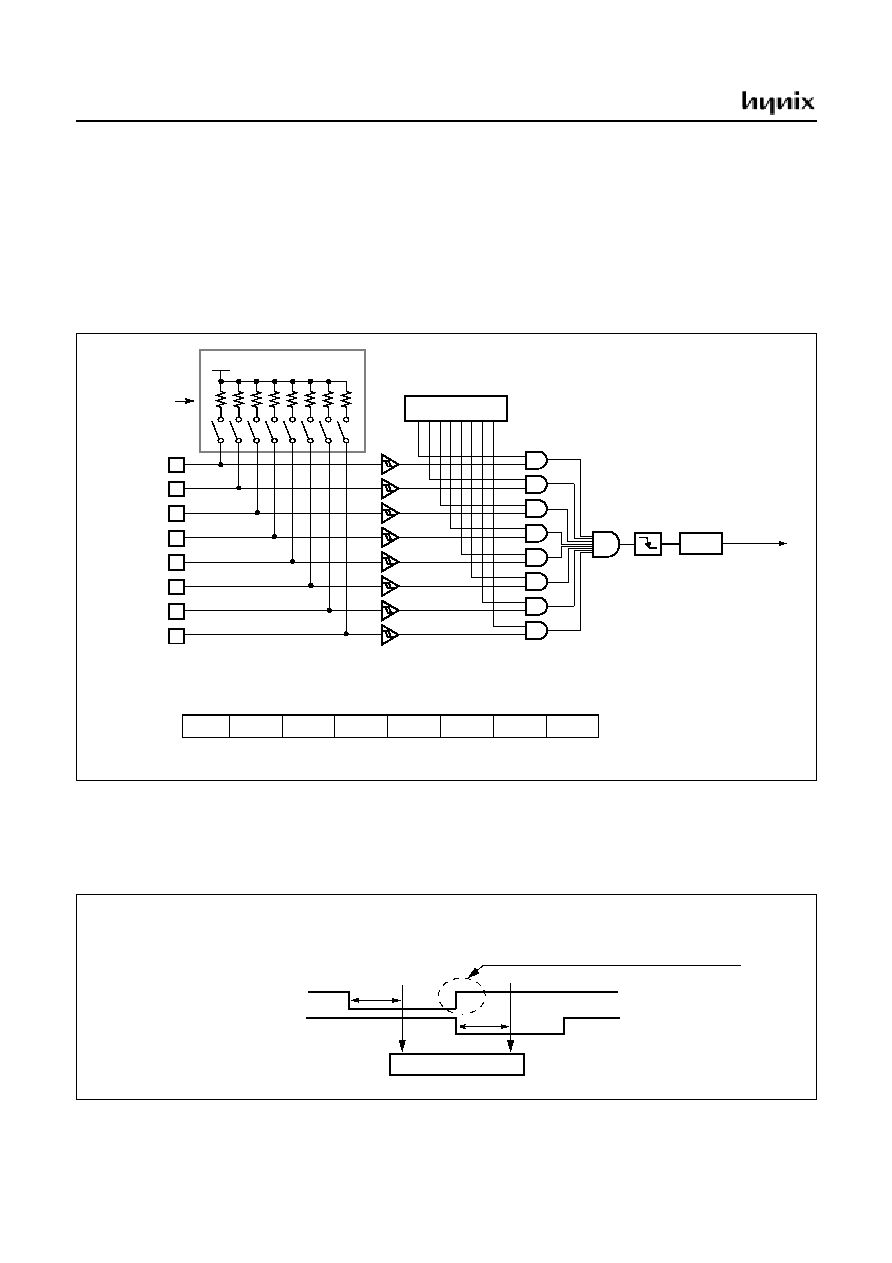
GMS81C5108
70
JUNE 2001 Ver 1.0
18. KEY SCAN
The key-scan block consists of key scan mode register
(KSMR) and R1 pull-up register (R1PU). When the key
scan interrupt is used, key scan mode register KSMR (ad-
dress 0F0
H
) should be set properly as shown in Figure 18-
1. The pins which is to be used as key scan input should be
set by KSMR and the strobe output pins should be set as
open drain. The strobe output pins could be selected from
among R0[7:0], R1[7:0], R2[3:0] and R3[3:0].
If the "L" signal is input to any one or more of key scan in-
put pins, the KSIF request flag is set to "1". This generates
an interrupt request. It also can be used in the way of re-
lease from STOP mode.
Figure 18-1 Key Scan Interrupt Block Diagram
Usage of Key Scan
When key board scanning, it is recommended that set the
output strobe to "L" first and then read R1 port after 60us
delay time. Because the rising time of the output strobe
port from "L" to "H" is so long. The Figure 18-2 explain
this reason.
Figure 18-2 Key Scan Timing
R13/KS3
R12/KS2
R11/KS1
R10/KS0
R1PU[7:0]
R17/KS7
R16/KS6
R15/KS5
R14/KS4
V
DD
KSMR
KSIF
Key Scan
Interrupt
KSMR (Key Scan Mode Register)
ADDRESS : 0F0
H
RESET VALUE : 00
H
Bit : 7 6 5 4 3 2 1 0
R/W
R/W
R/W
R/W
R/W
R/W
R/W
R/W
KS7
KS6
KS5
KS4
KS3
KS2
KS1
KS0
0 : Port Function (I/O) Selection
1 : Key Scan Input Selection
60
µ
s
R3<0>
R3<1>
60
µ
s
R1 Port Read Timing
If the rising time is so long, the key scanning could be
detected double key with R3<0> and R3<1>.
;Program Example,
LDM
CALL
LDA
;R3<0> Port set to low
;60us time delay routine
;read R1 port
R3,#0000_1110b
R1
Delay_60us
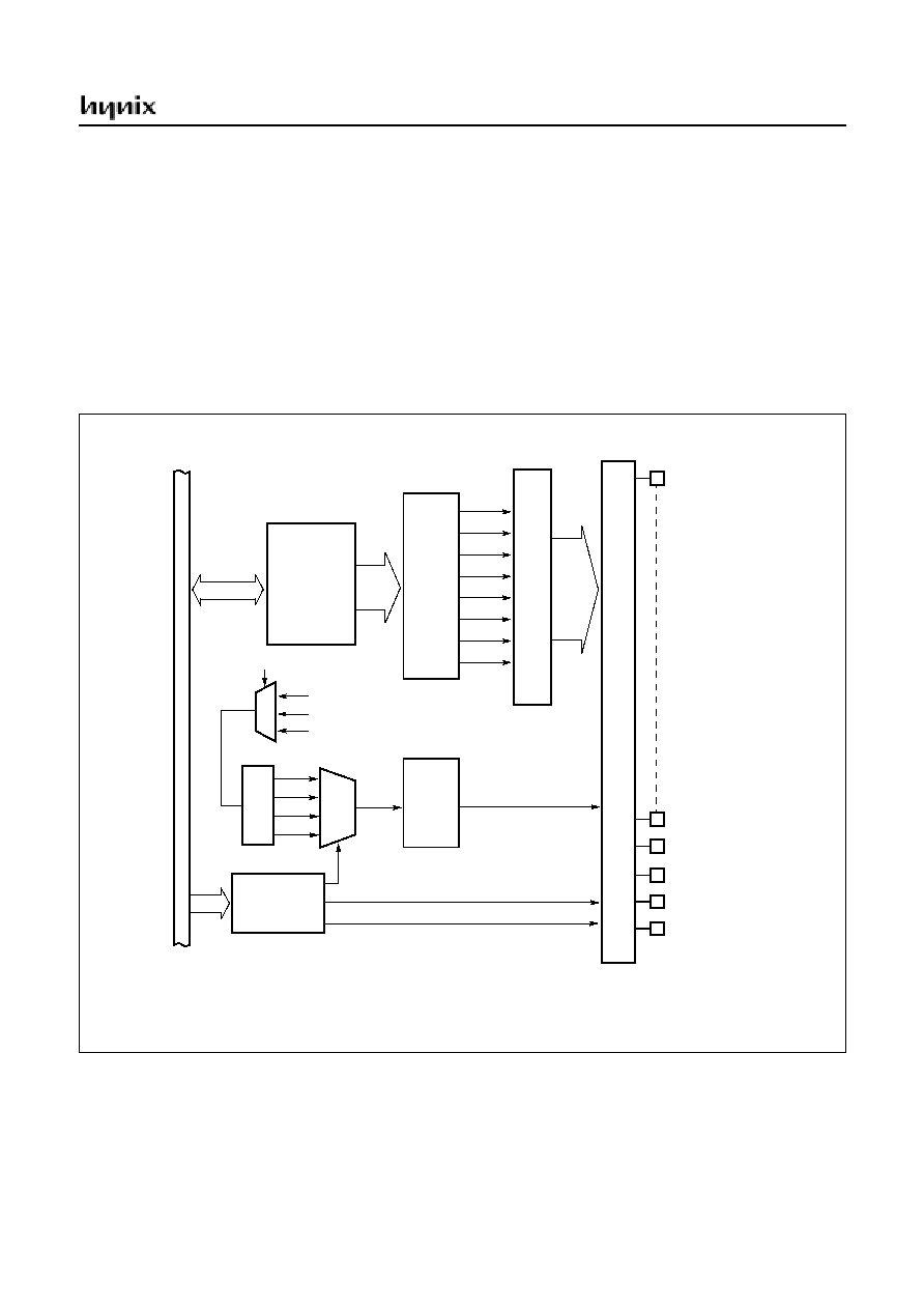
GMS81C5108
JUNE 2001 Ver 1.0
71
19. LCD DRIVER
The GMS81C5108 has the circuit that directly drives the
liquid crystal display (LCD) and its control circuit. The
Segment/Common Driver directly drives the LCD panel,
and the LCD Controller generates the segment/common
signals according to the RAM which stores display data. In
addition, VCL2 ~ VCL0 pin are provided as the drive pow-
er pins.
The GMS81C5108 has the following pins connected with
LCD.
1.
Segment output port 37 pins (SEG0-SEG36)
2.Common output port 4 pins (COM0-COM3)
19.1 Configuration of LCD driver
Figure 19-1 shows the configuration of the LCD driver.
Figure 19-1 LCD Driver Block Diagram
COM0
SEG34/COM3
SEG35/COM2
SEG36/COM1
SEG0
Di
spl
a
y
Data S
e
l
e
ct
Control
Di
sp
l
a
y Da
ta
Bu
ffe
r
re
g
i
s
t
e
r
LCD
Display Memory
S
egm
ent
/
C
om
m
on Driver
(37Nibbles)
÷
32
÷
64
÷
128
÷
256
Ti
mi
ng Cont
r
o
l
SEG33
Select clock
clock
LCR[0F1H]
LCD
LCDEN
INT
E
RNAL
BUS
L
I
NE
MUX
WTMR[1:0]
M U X
f
SUB
f
MAIN
00
10
Prescal
e
r
f
MAIN
÷
÷
÷
÷
2
7
01
Select Duty
Control Register
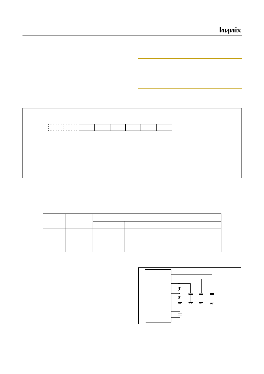
GMS81C5108
72
JUNE 2001 Ver 1.0
19.2 Control of LCD Driver Circuit
The LCD driver is controlled by the LCD Control Register
(LCR). The LCR[1:0] determines the frequency of COM
signal scanning of each segment output. RESET clears the
LCD control register LCR values to logic zero. The LCD
display can continue to operate during SLEEP and STOP
modes if a sub-frequency clock is used as system clock
source. The constant voltage booster circuit for using LCD
driver is built in, so the definite voltage could supplied re-
gardless of power source voltage fluctuations.
Note: The Sub clock is used as voltage booster source
clock, so the stabilization time is need to use voltage boost-
er. Normally, the stabilization time is need more than
500ms. The external bias registers cannot be used for LCD
display supply voltage.
Figure 19-2 LCD Control Register
Selecting Frame Frequency
Frame frequency is set to the base frequency as shown in
the following Table 19-1. The f
S
is selected to f
SUB
(sub
clock) which is 32.768kHz.
The matters to be attended to use LCD driver
In reset state, LCD source clock is sub clock. So, when the
power is supplied, the LCD display would be flickered be-
fore the oscillation of sub clock is stabilized. It is recom-
mended to use LCD display on after the stabilization time
of sub clock is considered enough. If the LCD is reset dur-
ing display, the display would be blotted by the capacity of
LCD power circuit. The external circuit of constant voltage
booster for using LCD driver is shown at right.
Figure 19-3 LCD Power Booster Circuit
LCDEN (LCD Display Enable Bit)
0: LCD Display Disable
1: LCD Display Enable
VBCL (Voltage Booster Enable Bit)
0: Voltage Booster Disable
1: Voltage Booster Enable
LCDD[1:0] (LCD Duty Selection)
00: 1/4 Duty
01: 1/3 Duty (COM[3] are used as SEG[34])
LCR(LCD Control Register)
ADDRESS : 0F1
H
RESET VALUE : --000000
B
-
-
LCDEN
VBCL
LCDD1
LCDD0
LCK1
LCK0
Bit : 7 6 5 4 3 2 1 0
R/W
R/W
R/W
R/W
R/W
R/W
LCK (LCD Clock source selection)
00: f
S
÷
32
01: f
S
÷
64
10: f
S
÷
128
11: f
S
÷
256
*
The fs can be selected among f
SUB
(Sub clock), f
MAIN
÷
2
7
(Main clck) and f
MAIN
(Main clock).
10: 1/2 Duty (COM[3:2] are used as SEG[34:35])
11: Static (COM[3:1] are used as SEG[34:36])
And sub or main is selected by WTCK[1:0] of WTMR.
LCR[1:0]
LCD clock
Frame Frequency (Hz)
Duty = Static
Duty = 1/2
Duty = 1/3
Duty = 1/4
00
01
10
11
f
S
÷
32
f
S
÷
64
f
S
÷
128
f
S
÷
256
1024
512
256
128
512
256
128
64
341.3
170.7
85.3
42.7
256
128
64
32
Table 19-1 Setting of LCD Frame Frequency
VCL2
VCL1
VCL0
R1
R2
C1
GMS81C5108
GMS87C5108
C2
C3
C4
CAPH
CAPL
C1~C4=0.47uF
R1=400K
R2=1M
GMS81C5108
JUNE 2001 Ver 1.0
73
19.3 LCD Display Memory
Display data are stored to the display data area (page 1) in
the data memory.
The display data stored to the display data area (address
0100
H
-0124
H
) are read automatically and sent to the LCD
driver by the hardware. The LCD driver generates the seg-
ment signals and common signals in accordance with the
display data and drive method. Therefore, display patterns
can be changed by only overwriting the contents of the dis-
play data area with a program. The table look up instruc-
tion is mainly used for this overwriting.
Figure 19.3 shows the correspondence between the display
data area and the SEG/COM pins. The LCD lights when
the display data is "1" and turn off when "0".
LCD display memory in this location that are not used for
LCD display can be allocated for general purpose use.
The SEG data for display is controlled by RPR (RAM Pag-
ing Register).
Figure 19-4 Setting of RAM Paging Register
Figure 19-5 LCD Display Memory
RPR (RAM Paging Register)
ADDRESS : 0F3
H
RESET VALUE : ------00
B
-
Bit : 7 6 5 4 3 2 1 0
R/W
R/W
R/W
R/W
-
-
RPR1
RPR0
-
-
RPR0
RAM Page Instruction
RPR1
x
0 Page
CLRG
x
0
0 Page
SETG
0
1
1 Page
SETG
0
-
SEG0
SEG1
SEG2
SEG3
SEG4
SEG5
SEG6
SEG7
COM
0
COM
1
COM
2
COM
3
SEG8
SEG9
SEG10
SEG11
SEG12
SEG13
SEG14
SEG15
SEG16
SEG17
SEG18
SEG19
SEG20
SEG21
SEG22
SEG23
SEG24
SEG25
SEG26
SEG27
SEG28
SEG29
SEG30
SEG31
SEG32
SEG33
SEG34
SEG35
SEG36
0
1
2
3
4
5
6
7
Bit
0100
H
0101
H
0102
H
0103
H
0104
H
0105
H
0106
H
0107
H
0108
H
0109
H
010A
H
010B
H
010C
H
010D
H
010E
H
010F
H
0110
H
0111
H
0112
H
0113
H
0114
H
0115
H
0116
H
0117
H
0118
H
0119
H
011A
H
011B
H
011C
H
011D
H
011E
H
011F
H
0120
H
0121
H
0122
H
0123
H
0124
H
GMS81C5108
74
JUNE 2001 Ver 1.0
19.4 Control Method of LCD Driver
Initial Setting
Flow chart of initial setting is shown in Figure 19-6.
Example: Driving of LCD
.
Figure 19-6 Initial Setting of LCD Driver
Figure 19-7 Example of Connection COM & SEG
Display Data
Normally, display data are kept permanently in the pro-
gram memory and then stored at the display data area by
the table look-up instruction. This can be explained using
character display with 1/4 duty LCD as an example as well
as any LCD panel. The COM and SEG connections to the
LCD and display data are the same as those shown is Fig-
ure 19-7. Following is showing the Programming example
for displaying character.
Note: When power on RESET, sub oscillation start up time
is required. Enable LCD display after sub oscillation is sta-
bilized, or LCD may occur flicker at power on time shortly.
Clear
LCD Display
Memory
Select Frame Frequency
Turn on LCD
LDM
LCR,#12H
;f
F
=64Hz, 1/4 duty
(f
SUB
= 32.768kHz)
:
LDM
RPR,#1
;Select LCD Memory(1 page)
SETG
LDX
#0
C_LCD1:
LDA
#0
;RAM Clear
;(0100H->0124H)
STA
{X}+
CMPX
#025H
BNE
C_LCD1
CLRG
:
SET1
LCR.5
;Enable display
:
Setting of LCD drive method
Initialize of display memory
Enable display
SEG0
SEG1
COM3
COM0
COM1
COM2
Example: display "2"
1
1
1
0
0
1
0
1
*
*
*
*
*
*
*
*
100
H
101
H
3
1
2
0
bit 7
5
6
4
Note: * are don't care.
GMS81C5108
JUNE 2001 Ver 1.0
75
LCD Waveform
The LCD duty can be selected by LCR register. The kinds
of LCD waveforms are four totally. Among them, static
and 1/4 duty waveforms are shown Figure 19-8.
Figure 19-8 Example of LCD drive output
:
CLRG
LDX
#<DISPRAM
;Address included the data
;to be displayed.
GOLCD:
LDA
{X}
TAY
LDA
!FONT+Y
;LOAD FONT DATA
LDM
RPR,#1
;Set RPR = 1 to access LCD
SETG
;Set Page 1
LDX
#0
STA
{X}+
;LOWER 4 BITS OF ACC. seg0
XCN
STA
{X}
;UPPER 4 BITS OF ACC. seg1
CLRG
;Set Page = 0
:
FONT
DB
1101_0111B
; "0"
DB
0000_0110B
; "1"
DB
1110_0011B
; "2"
DB
1010_0111B
; "3"
DB
0011_0110B
; "4"
DB
1011_0101B
; "5"
DB
1111_0101B
; "6"
DB
0000_0111B
; "7"
DB
1111_0111B
; "8"
DB
0011_0111B
; "9"
Font data
Write into the
LCD Memory
COM0
COM1
SEG0
SEG1 - COM0
SEG1
COM2
COM3
GND
VCL1
VCL0
1/4 Duty, 1/3 Bias Drive
SEG0 - COM0
0
VCL0
VCL1
VCL2
-VCL2
-VCL1
-VCL0
GND
VCL0
VCL1
VCL2
GND
VCL0
VCL1
VCL2
GND
VCL0
VCL1
VCL2
GND
VCL1
VCL0
VCL2
GND
VCL0
VCL1
VCL2
0
VCL0
VCL1
VCL2
-VCL2
-VCL1
-VCL0
VCL2
COM
0
COM
1
COM
2
COM
3
SEG0
SEG1
SEG0
SEG1
COM3
COM0
COM1
COM2
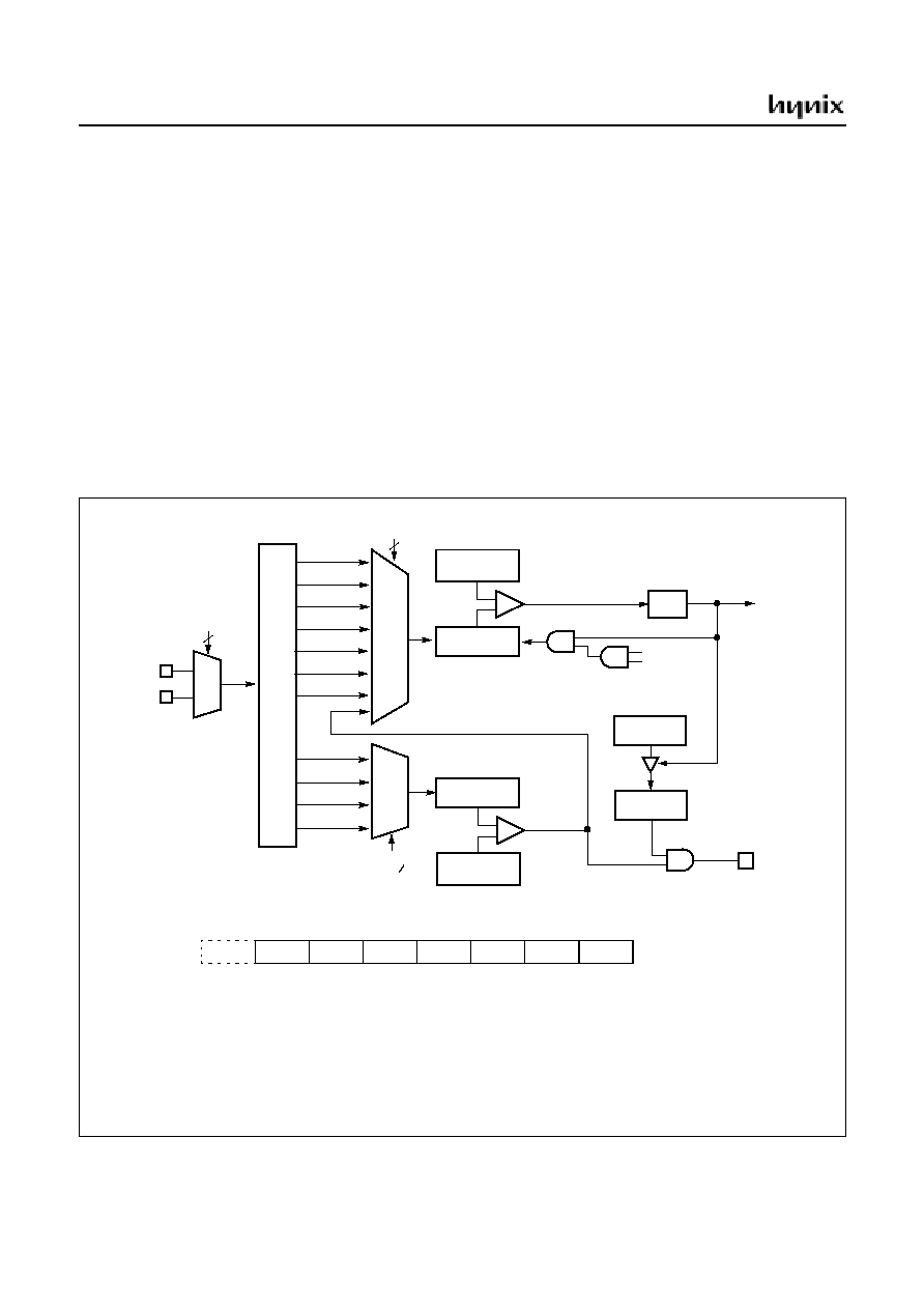
GMS81C5108
76
JUNE 2001 Ver 1.0
20. REMOCON CARRIER GENERATOR
The GMS81C5108 has a circuit to generate carriers for the
remote controller. This circuit consists of Remocon Mode
Register (RMR), Carrier Frequency High Selection (CF-
HS), Carrier Frequency Low Selection (CFLS), Remocon
Data High Register (RDHR), Remocon Data Low Register
(RDLR), Remocon Data Counter (RDC), Remocon Output
Data Register (RODR) and Remocon Output Buffer
(ROB) as shown in Figure 20-1. A carrier duty and fre-
quency are determined by the contents of these registers. A
source clock input to the 6-bit counter is selected by diving
the frequency of the system clock by two (main or sub
clock).
20.1 Remocon Signal Output Control
The output of the REMOUT pin which outputs carriers is
controlled by RODR and ROB register. While the Bit-0 of
RODR is "1", the REMOUT pin outputs a carrier signal
generated by the remote controller carrier generator. While
this Bit is "0", the output of the REMOUT pin is low.
The content of the ROB is automatically transferred to the
RODR by an interrupt signal generated by the 8-Bit timer.
The content of the RODR.0 is output to the REMOUT pin.
Namely, the REMOUT pin outputs a high-level signal
when RODR.0 is "1" and a low-level signal when RODR.0
is "0".
Figure 20-1 Remocon Carrier Generator Block Diagram
SCMR[1:0]
2
0X
1X
X
IN
SX
IN
Pre-
scaler
RDCK[2:0]
fxin
÷
8
fxin
÷
16
2
REN
0
& CCK[1:0]
Remocon
REMF
Interrupt
fxin
÷
32
fxin
÷
64
fxin
÷
128
fxin
÷
256
fxin
÷
512
fxin
÷
1
fxin
÷
2
fxin
÷
4
fxin
÷
8
MUX
MUX
REN
0
6-Bit Counter
CFHS (6-Bit)
CFLS (6-Bit)
Comparator
RDC(8Bit)
RDHR (8-Bit)
RDLR (8-Bit)
Comparator
RDPE
REN
ROB (1Bit)
RODR (1Bit)
REMOUT
RMR (Remocon Mode Register)
ADDRESS : 0F6
H
RESET VALUE : -0000000
B
-
REN
CCK1
CCK0
RDPE
RDCK2
RDCK1
RDCK0
Bit : 7 6 5 4 3 2 1 0
R/W
R/W
R/W
R/W
R/W
R/W
R/W
REN (Remocon Operation Enable)
0 : Disable
RDCK[2:0] (Remocon Data Clock Selection)
CCK[1:0] (Carrier Clock Source Selection)
1 : Enable
RDPE (Remocon Data Pulse Enable)
0 : Disable
1 : Enable
111: Carrier Signal
fxin is f
MAIN
or f
SUB.
000: f
MAIN
÷
2
3
001: f
MAIN
÷
2
4
010: f
MAIN
÷
2
5
011: f
MAIN
÷
2
6
100: f
MAIN
÷
2
7
101: f
MAIN
÷
2
8
110: f
MAIN
÷
2
9
f
MAIN
: main-clock frequency
f
SUB
: sub-clock frequency
or f
SUB
÷
2
4
or f
SUB
÷
2
3
or f
SUB
÷
2
6
or f
SUB
÷
2
5
or f
SUB
÷
2
7
or f
SUB
÷
2
9
or f
SUB
÷
2
8
00: f
MAIN
01: f
MAIN
÷
2
10: f
MAIN
÷
2
2
11: f
MAIN
÷
2
3
or f
SUB
÷
2
or f
SUB
or f
SUB
÷
2
3
or f
SUB
÷
2
2
GMS81C5108
JUNE 2001 Ver 1.0
77
Figure 20-2 Remocon Registers
20.2 Carrier Frequency
The carrier frequency and the pulse of data are calculated
by below formula. The the lengths of carrier frequency and
pulse of data are shown in Figure 20-3.
t
H
= source clock(RMR[5:4])
×
CFHS
t
L
= source clock(RMR[5:4])
×
CFHS
f
C
(Carrier Frequency) = 1/(t
H
+t
L
)
t
DH
= source clock(RMR[2:0])
×
RDHR
t
DL
= source clock(RMR[2:0])
×
RDLR
CFHS (Carrier Frequency High Selection)
ADDRESS : 0F7
H
-
-
CFH5
CFH4
CFH3
CFH2
CFH1
CFH0
Bit : 7 6 5 4 3 2 1 0
W
W
W
W
W
W
RDHR (Remocon Data High Register)
ADDRESS : 0F9
H
RDH7
RDH6
RDH5
RDH4
RDH3
RDH2
RDH1
RDH0
Bit : 7 6 5 4 3 2 1 0
W
W
W
W
W
W
W
W
RESET VALUE : --111111
B
Carrier High Interval = The Value of CFHS x Clock Source Period
CFLS (Carrier Frequency Low Selection)
ADDRESS : 0F8
H
-
-
CFL5
CFL4
CFL3
CFL2
CFL1
CFL0
Bit : 7 6 5 4 3 2 1 0
W
W
W
W
W
W
RESET VALUE : --111111
B
Carrier Low Interval = The Value of CFLS x Clock Source Period
RESET VALUE : 11111111
B
Remocon Data High Interval = The Value of RDHR x Clock Source Period
RDLR (Remocon Data Low Register)
ADDRESS : 00FA
H
RDL7
RDL6
RDL5
RDL4
RDL3
RDL2
RDL1
RDL0
Bit : 7 6 5 4 3 2 1 0
W
W
W
W
W
W
W
W
RESET VALUE : 11111111
B
Remocon Data Low Interval = The Value of RDLR x Clock Source Period
RDC (Remocon Data Counter)
ADDRESS : 00FA
H
RDC7
RDC6
RDC5
RDC4
RDC3
RDC2
RDC1
RDC0
Bit : 7 6 5 4 3 2 1 0
R
R
R
R
R
R
R
R
RESET VALUE : 00000000
B
Remocon Data Counter Value
RODR (Remocon Output Data Register)
ADDRESS : 0FB
H
-
-
-
-
-
-
-
RDD0
Bit : 7 6 5 4 3 2 1 0
R/W
RESET VALUE : -------0
B
Remocon Data Output Value
ROB (Remocon Output Buffer)
ADDRESS : 0FC
H
-
-
-
-
-
-
-
RDB0
Bit : 7 6 5 4 3 2 1 0
R/W
RESET VALUE : -------0
B
Remocon Data Output Buffer
GMS81C5108
78
JUNE 2001 Ver 1.0
Figure 20-3 Carrier Frequency & Pulse of Data
The Table 20-1 shows high and low length of carrier fre-
quency according to CFLS and CFHS. This only shows
when the source clock is selected f
MAIN
and f
MAIN
÷2
2
at
4MHz.
Table 20-1 Length of Carrier Frequency (at 4MHz)
ROD0 = 01
H
ROD0 = 00
H
t
DL
t
DH
As soon as the carrier interrupt is occurred,
the content of ROB is transferred to RODR.
t
H
t
L
Carrier Frequency
Pulse of Data
Set Value
Selection of PS0
Selection of PS2
Set Value
Selection of PS0
Selection of PS2
CFHS
CFLS
t
H
(us)
t
L
(us)
t
H
(us)
t
L
(us)
CFHS
CFLS
t
H
(us)
t
L
(us)
t
H
(us)
t
L
(us)
00
H
01
H
02
H
03
H
04
H
05
H
06
H
07
H
08
H
09
H
0A
H
0B
H
0C
H
0D
H
0E
H
0F
H
10
H
11
H
12
H
13
H
14
H
15
H
16
H
17
H
18
H
19
H
1A
H
1B
H
1C
H
1D
H
1E
H
1F
H
00
H
01
H
02
H
03H
04
H
05
H
06
H
07
H
08
H
09
H
0A
H
0B
H
0C
H
0D
H
0E
H
0F
H
10
H
11
H
12
H
13
H
14
H
15
H
16
H
17
H
18
H
19
H
1A
H
1B
H
1C
H
1D
H
1E
H
1F
H
-
0.25
0.50
0.75
1.00
1.25
1.50
1.75
2.00
2.25
2.50
2.75
3.00
3.25
3.50
3.75
4.00
4.25
4.50
4.75
5.00
5.25
5.50
5.75
6.00
6.25
6.50
6.75
7.00
7.25
7.50
7.75
-
0.25
0.50
0.75
1.00
1.25
1.50
1.75
2.00
2.25
2.50
2.75
3.00
3.25
3.50
3.75
4.00
4.25
4.50
4.75
5.00
5.25
5.50
5.75
6.00
6.25
6.50
6.75
7.00
7.25
7.50
7.75
-
1.00
2.00
3.00
4.00
5.00
6.00
7.00
8.00
9.00
10.00
11.00
12.00
13.00
14.00
15.00
16.00
17.00
18.00
19.00
20.00
21.00
22.00
23.00
24.00
25.00
26.00
27.00
28.00
29.00
30.00
31.00
-
1.00
2.00
3.00
4.00
5.00
6.00
7.00
8.00
9.00
10.00
11.00
12.00
13.00
14.00
15.00
16.00
17.00
18.00
19.00
20.00
21.00
22.00
23.00
24.00
25.00
26.00
27.00
28.00
29.00
30.00
31.00
20
H
21
H
22
H
23
H
24
H
25
H
26
H
27
H
28
H
29
H
2A
H
2B
H
2C
H
2D
H
2E
H
2F
H
30
H
31
H
32
H
33
H
34
H
35
H
36
H
37
H
38
H
39
H
3A
H
3B
H
3C
H
3D
H
3E
H
3F
H
20
H
21
H
22
H
23
H
24
H
25
H
26
H
27
H
28
H
29
H
2A
H
2B
H
2C
H
2D
H
2E
H
2F
H
30
H
31
H
32
H
33
H
34
H
35
H
36
H
37
H
38
H
39
H
3A
H
3B
H
3C
H
3D
H
3E
H
3F
H
8.00
8.25
8.50
8.75
9.00
9.25
9.50
9.75
10.00
10.25
10.50
10.75
11.00
11.25
11.50
11.75
12.00
12.25
12.50
12.75
13.00
13.25
13.50
13.75
14.00
14.25
14.50
14.75
15.00
15.25
15.50
15.75
8.00
8.25
8.50
8.75
9.00
9.25
9.50
9.75
10.00
10.25
10.50
10.75
11.00
11.25
11.50
11.75
12.00
12.25
12.50
12.75
13.00
13.25
13.50
13.75
14.00
14.25
14.50
14.75
15.00
15.25
15.50
15.75
32.00
33.00
34.00
35.00
36.00
37.00
38.00
39.00
40.00
41.00
42.00
43.00
44.00
45.00
46.00
47.00
48.00
49.00
50.00
51.00
52.00
53.00
54.00
55.00
56.00
57.00
58.00
59.00
60.00
61.00
62.00
63.00
32.00
33.00
34.00
35.00
36.00
37.00
38.00
39.00
40.00
41.00
42.00
43.00
44.00
45.00
46.00
47.00
48.00
49.00
50.00
51.00
52.00
53.00
54.00
55.00
56.00
57.00
58.00
59.00
60.00
61.00
62.00
63.00

GMS81C5108
JUNE 2001 Ver 1.0
79
Example:
Carrier Frequency = 37.8kHz, high = 8.52ms, low = 4.24ms, @4MHz
Rem_sig: LDM
RMR,#0001_0010B ;carrier clock(PS1), remocon data clock(PS5)
LDM
CFHS,#18
;carrier low(IR LED)=18*PS1(0.5us)=9us
LDM
CFLS,#35
;carrier high(IR LED)=35*PS1(0.5us)=17.5us
CLR1
ROD0
LDM
R_bit,#1111_1000B
LDM
RDHR,#213
;213*5*PS5(8us)=8.52ms
LDM
RDLR,#177
;177*3*PS5(8us)=4.248ms
LDX
#9
CALL
DATA
SET1
RMR.6
;Remocon operation enable
SET1
RMR.3
;Remocon data pulse enable
SET1
IENL.6
;Remocon int.
Loop1:
NOP
CMPX
#0
BNE
Loop1
Finish:
CLR1
ROD0
CLR1
ROB0
RET
;********
Data:
ROL
R_bit
BCS
Set_rob0
CLR1
ROB0
RET
Set_rob0:SET1ROB0
RET
;***********************************************;
; Remocon int service routine ;
;***********************************************;
;
Remocon_INT:
CALL
Data
DEC
X
RETI
GMS81C5108
80
JUNE 2001 Ver 1.0
21. OSCILLATOR CIRCUIT
The GMS81C5108 has two oscillation circuits internally.
X
IN
and X
OUT
are input and output for main frequency and
SX
IN
and SX
OUT
are input and output for sub frequency,
respectively, inverting amplifier which can be configured
for being used as an on-chip oscillator, as shown in Figure
21-1.
Figure 21-1 Oscillation Circuit
Oscillation circuit is designed to be used either with a ce-
ramic resonator or crystal oscillator. Since each crystal and
ceramic resonator have their own characteristics, the user
should consult the crystal manufacturer for appropriate
values of external components.
In addition, see Figure 21-2 for the layout of the crystal.
Note: Minimize the wiring length. Do not allow the wiring to
intersect with other signal conductors. Do not allow the wir-
ing to come near changing high current. Set the potential of
the grounding position of the oscillator capacitor to that of
V
SS
. Do not ground it to any ground pattern where high cur-
rent is present. Do not fetch signals from the oscillator.
Figure 21-2 Layout of Oscillator PCB circuit
X
OUT
X
IN
V
SS
Recommend
C1,C2 = 20pF
C1
C2
X
OUT
X
IN
External Clock
Open
X
OUT
X
IN
External Oscillator
RC Oscillator
Crystal or Ceramic Oscillator
SX
OUT
SX
IN
V
SS
Recommend
C3,C4 = 30pF
C3
C4
32.768KHz
4.19MHz
Crystal Oscillator
Ceramic Resonator
C1,C2 = 20pF
Select R value according to AC Characteristics.
R
EXT
The Cap. is built in(5pF).
X
OUT
X
IN
GMS81C5108
JUNE 2001 Ver 1.0
81
22. RESET
The GMS81C5108 have two types of reset generation pro-
cedures; one is an external reset input, the other is a watch-
dog timer reset. Table 22-1 shows on-chip hardware ini-
tialization by reset action.
Table 22-1 Initializing Internal Status by Reset Action
22.1 External Reset Input
The reset input is the RESET pin, which is the input to a
Schmitt Trigger. A reset in accomplished by holding the
RESET pin to low for at least 8 oscillator periods, within
the operating voltage range and oscillation stable, it is ap-
plied, and the internal state is initialized. After reset,
65.5ms (at 4MHz) add with 7 oscillator periods are re-
quired to start execution as shown in Figure 22-2.
Internal RAM is not affected by reset. When V
DD
is turned
on, the RAM content is indeterminate. Therefore, this
RAM should be initialized before read or tested it.
When the RESET pin input goes to high, the reset opera-
tion is released and the program execution starts at the vec-
tor address stored at FFFE
H
- FFFF
H
.
A connection for simple power-on-reset is shown in Figure
22-1.
Figure 22-1 Simple Power-on-Reset Circuit
Figure 22-2 Timing Diagram after RESET
22.2 Watchdog Timer Reset
Refer to "13.2 Watch Dog Timer" on page 57.
On-chip Hardware
Initial Value
On-chip Hardware
Initial Value
Program counter
(PC)
(FFFF
H
) - (FFFE
H
)
Peripheral clock
On
RAM page register
(RPR)
0
SVD
Enable
G-flag
(G)
0
Control registers
Refer to Table 8-1 on page 25
Operation mode
Main-frequency clock
Voltage Booster
Disable
RESET
+
-
V
DD
V
DD
GND
Mask Option
MCU
100k
1uF
MAIN PROGRAM
System Clock
?
?
FFFE FFFF
Stabilization Time
t
ST
= 65.5mS at 4MHz
RESET
ADDRESS
DATA
1
2
3
4
5
6
7
?
?
Start
?
?
?
FE
?
ADL
ADH
OP
BUS
BUS
RESET Process Step
~~
~~
~~
~~
~~
~~
t
ST
=
x 256
f
MAIN
÷
1024
1
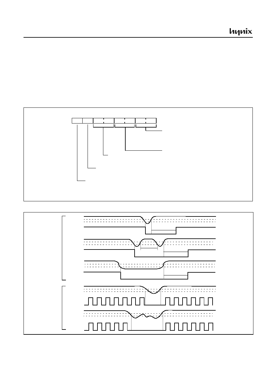
GMS81C5108
82
JUNE 2001 Ver 1.0
23. SUPPLY VOLTAGE DETECTION
The GMS81C5108 has an on-chip low voltage detection
circuitry to detect the V
DD
voltage. A configuration regis-
ter, SCMR, can enable or disable the low voltage detect
circuitry. This GMS81C5108 has two level detec-
tor(SVD0, SVD1). The SVD0 flag is set when the V
DD
falls below 2.2V and if the V
DD
is rise above 2.2V the
SVD0 is cleared automatically. The SVD1 flag is set when
the V
DD
falls below 1.7V and if this flag is set once, it is
not cleared automatically although the V
DD
rises above
1.7V. It can be cleared by writing.
If the SVD1 is set, the MCU can be RESET or frozen by
the flag SVRT. In the in-circuit emulator, supply voltage
detection is not implemented and user can not experiment
with it. Therefore, after final development of user program,
this function may be experimented or evaluated.
Figure 23-1 Low Voltage Detector Register
Figure 23-2 Power Fail Processor Situations
* The values of 1.7V and 2.2V could be changed by ±0.2V according to the process of work.
R/W
R/W
R/W
R/W
SYCC[1:0] (System clock control)
00: main clock on
01: main clock on
10: sub clock on (main clock on)
11: sub clock on (main clock off)
SCS[1:0] (System clock source select)
INITIAL VALUE: 00
H
ADDRESS: 0F5
H
SCMR (System
MSB
LSB
R/W
R/W
R/W
R
SVD[1:0] (SVD Flag)
SVD0 : set at VDD=2.2V
SVD1 : set at VDD=1.7V
SVRT (System Reset Control by SVD1 Bit)
0 : System reset by SVD1 Flag
1 : Don't system reset by SVD1 Flag (Freeze)
SVEN (SVD Operation Enable Bit)
0 : SVD Operation Enable
1 : SVD Operation Disable
Clock Mode Register)
f
MAIN
÷
2
4
f
MAIN
÷
2
3
f
MAIN
÷
2
f
MAIN
÷
2
6
or f
SUB
÷
2
or f
SUB
÷
2
3
or f
SUB
÷
2
6
or f
SUB
÷
2
4
Internal
RESET
Internal
RESET
Internal
RESET
V
DD
V
DD
V
DD
SVD
MAX
SVD MIN
SVD MAX
SVD MIN
SVD MAX
SVD MIN
65.5mS
65.5mS
t < 65.5mS
65.5mS
When SVRT = 0
V
DD
V
DD
SVD MAX
SVD MIN
SVD MAX
SVD MIN
When SVRT = 1
System
Clock
System
Clock
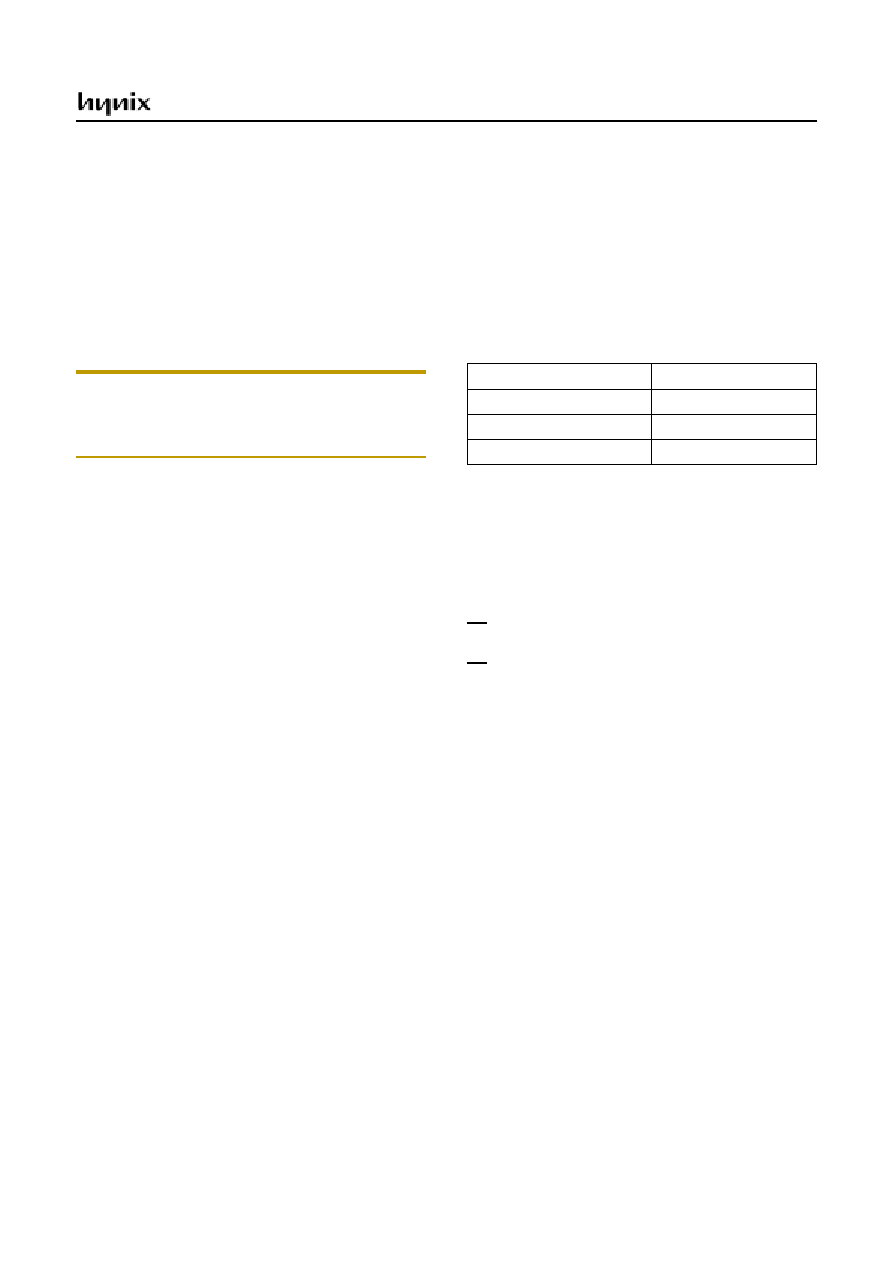
GMS81C5108
JUNE 2001 Ver 1.0
83
24. DEVEMOPMENT TOOLS
24.1 OTP Programming
The GMS87C5108 is an OTP (One Time Programmable) micro-
controllers. Its internal user memory is constructed with EPROM
(Electrically Programmable Read Only Memory).
The OTP microcontroller is generally used for chip evaluation,
first production, small amount production, fast mass production,
etc.
Blank OTP's internal EPROM is filled by 00
H
, not FF
H
.
Note: In any case, you have to use the *.OTP file for pro-
gramming, not the *.HEX file. After assemble, both OTP
and HEX file are generated by automatically. The HEX file
is used during program emulation on the emulator.
How to Program
To program the OTP devices, user can use Hynix own program-
mer.
Hynix
own programmer list
Manufacturer: Hynix Semiconductor Programmer:
Choice-Sigma
Choice-Gang4
The Choice-Sigma is a Hynix Universal Single Programmer for
all of Hynix OTP devices, also the Choice-Gang4 can program
four OTPs at once for Hynix OTP.
Ask to Hynix sales part for purchasing or more detail
Programming Procedure
1. Select device
GMS87C5108
you want.
2. Load the *.OTP file from the PC. The file is composed
of Motorola-S1 format.
3. Set the programming address range as below table.
4. Mount the socket adapter on the programmer.
5. Start program/verify.
Pin Function
V
PP
(Program Voltage)
V
PP
is the input for the program voltage for programming the
EPROM.
CE (Chip Enable)
CE is the input for programming and verifying internal EPROM.
OE (Output Enable)
OE is the input of data output control signal for verify.
A0~A15 (Address Bus)
A0~A15 are address input pins for internal EPROM.
O0~O7 (EPROM Data Bus)
These are data bus for internal EPROM.
Address
Set Value
Buffer start address
E000
H
Buffer end address
FFFF
H
Device start address
E000
H
GM
S81C51
08
84
JU
NE 2001
Ver
1.0
24
.2 Emulat
or S/W Sett
ing
POWER
RUN
STOP
SLEEP
CHO
ICE-
D
r
.
EV
A 81C51
B/D Rev 1.0
S
/
N
.
-
-
-
-
-
---
--
--
--
-
CONNECTA
CONNECTB
CONNECTC
J_USERB
RESET
J_USERA
V_USER
X1 (OSC)
X2
/RESET
XOUT
LC
D
_
V
D
D
VLC
D
C
SEG46
SEG44
SEG42
SEG40
SEG38
VREG
COM1/S36
COM3/S34
SEG32
SEG30
SEG28
SEG26
SEG24
SEG22
SEG20
SEG18
SEG16
SEG14
SEG12
SEG10
SEG8
SEG6
SEG4
SEG2
SEG0
SEG47
SEG45
SEG43
SEG41
SEG39
SEG37
COM0
COM2/S35
SEG33
SEG31
SEG29
SEG27
SEG25
SEG23
SEG21
SEG19
SEG17
SEG15
SEG13
SEG11
SEG9
SEG7
SEG5
SEG3
SEG1
GND
VCL1
VLCDC
CB
GND
REMOUT (TONED)
GND
R36
R34
R21
R23
R25
R27
R16
R14
R12
R10
R06
R04
R02
R00
R32
R30
+5V
GND
VCL0
VCL2
CA
GND
/U_RST
U_XOUT
GND
R37
R35
R20
R22
R24
R26
R17
R15
R13
R11
R07
R05
R03
R01
R33
R31
+5V
J_USERB
J_USERA
SW
4
SW
5
Ex
te
rn
a
l
O
s
c
illa
t
o
r
Socket
GM
S8
1C
51
EVA
+5
V
SW
2
2 1
OFF ON
O
FF O
N
SW
1
VR1
VR2
1
2
3
4
5
6
7
1
2
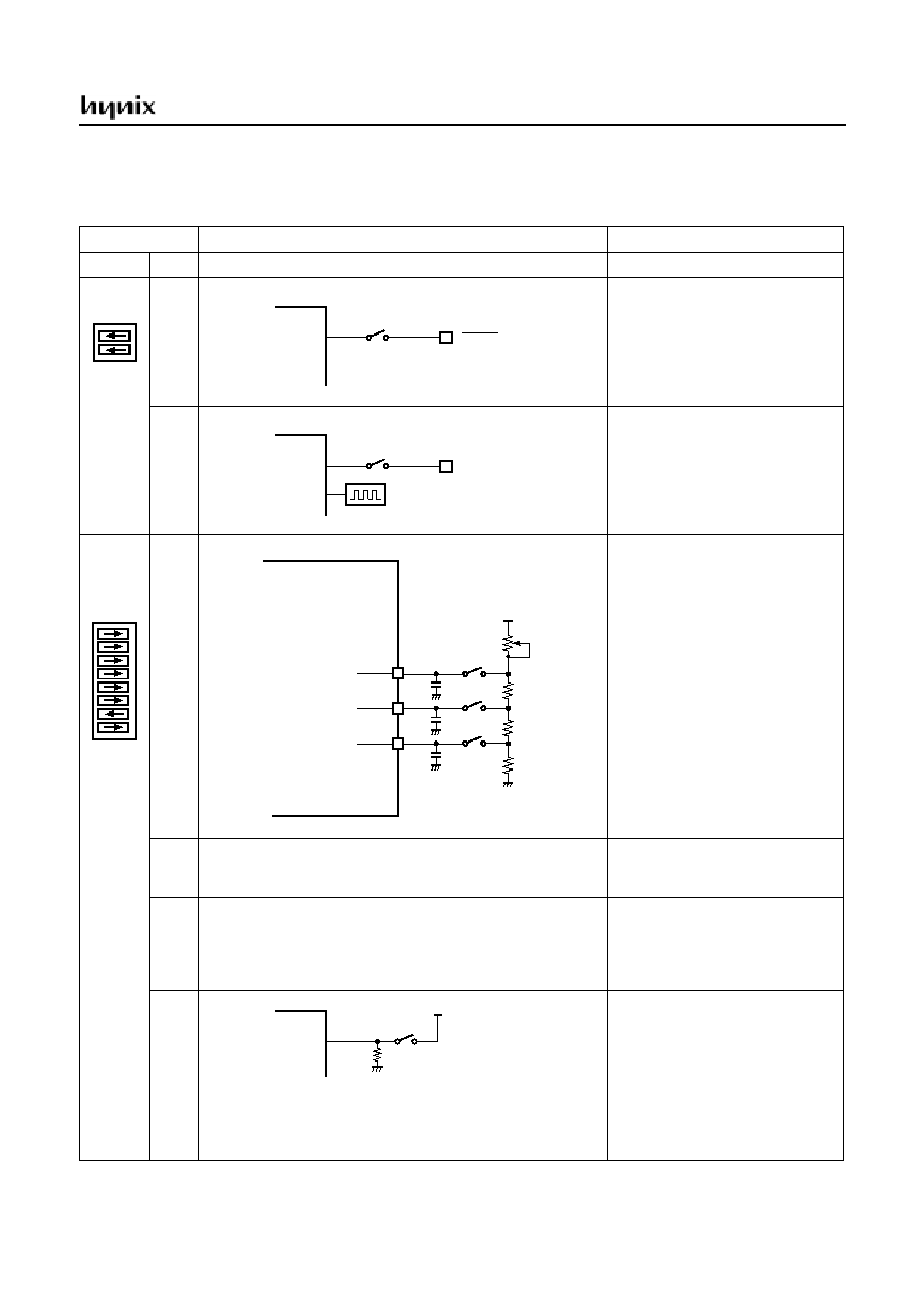
GMS81C5108
JUNE 2001 Ver 1.0
85
DIP Switch and VR Setting
Before execute the user program, keep in your mind the below configuration
DIP S/W, VR
Description
ON/OFF Setting
SW1
-
Emulator Reset Switch. Reset the Emulator.
Reset the Emulator.
SW2
1
Normally OFF.
EVA. chip can be reset by external
user target system board.
ON : Reset is available by user
target system board.
OFF : MCU is reset by REST switch
on EVA. board.
2
Normally OFF.
MCU XOUT pin are disconnected
by Emulator internally. Some cir-
cumstance user may connect this
circuit.
ON : Output XOUT signal
OFF : Disconnect circuit
SW4
1
2
3
Normally ON.
It serves the external bias resistors.
If user want to use external circuit
instead of internal R, turn on these
switches.
4
5
6
LCD Voltage booster circuit.
Must be ON position.
It is used for the GMS81C5108.
7
Select the Stack Page.
Must be OFF position.
This switch decide the Stack page 0
(off) or page 1 (on).
ON : For the GMS81C7XXX
OFF : For the GMS81C5108
8
GMS81C5108 detect the V
DD
voltage but Emulator can not do
because Emulator can not operate if V
DD
is below normal opr.
voltage (5V), This switch serves LVD environment through the
applying 0V to LVD pin of EVA. chip during 5V normal operation.
Position ON during normal opera-
tion.
ON : Normal operation
OFF : Force to detect the LVD, refer
to "23. SUPPLY VOLTAGE DETEC-
TION" on page 82.
SW2-1
RESET pin
EVA.
Chip
SW2-2
XOUT pin
EVA.
Chip
Oscillator
VCL1
VCL2
External Resistor
VCL0
V
SS
V
DD
Adjust Contrast
SW4-1
SW4-2
SW4-3
0.47uF
×
3
10k
×
3
and Capacitor
VR1 50k
SW4-8
V
DD
EVA.
Chip
LVD pin
OFF ON
OFF ON

GMS81C5108
86
JUNE 2001 Ver 1.0
SW5
1
Internal power supply to sub-oscillation circuit.
Must be ON position.
2
Reserved for other purpose.
Must be OFF position.
VR1
-
Adjust the LCD contrast. It control the VCL2 voltage.
Refer to above SW4-1,2,3 figure.
Adjust the proper position as well as
LCD display good.
VR2
-
Reserved for other purpose.
Don't care.
DIP S/W, VR
Description
ON/OFF Setting
OFF ON

GMS81C5108
JUNE 2001 Ver 1.0
87
Book History
This Book Ver 1.0 (JUNE 2001)
First edition.

APPENDIX
GMS81C5108 APPENDIX
JUNE 2001 Ver 1.0
i
A. CONTROL REGISTER LIST
Address
Register Name
Symbol
R/W
Initial Value
Page
7 6 5 4 3 2 1 0
00C0
R0 port data register
R0
R/W
0 0 0 0 0 0 0 0
32
00C1
R1 port data register
R1
R/W
0 0 0 0 0 0 0 0
32
00C2
R2 port data register
R2
R/W
- - - - 0 0 0 0
33
00C3
R3 port data register
R3
R/W
- - - - 0 0 0 0
33
00C8
R0 port I/O direction register
R0DR
W
0 0 0 0 0 0 0 0
32
00C9
R1 port I/O direction register
R1DR
W
0 0 0 0 0 0 0 0
32
00CA
R2 port I/O direction register
R2DR
W
- - - - 0 0 0 0
33
00CB
R3 port I/O direction register
R3DR
W
- - - - 0 0 0 0
33
00D0
R0 port pull-up register
R0PU
W
0 0 0 0 0 0 0 0
32
00D1
R1 port pull-up register
R1PU
W
0 0 0 0 0 0 0 0
32
00D2
R2 port pull-up register
R2PU
W
- - - - 0 0 0 0
33
00D3
R3 port pull-up register
R3PU
W
- - - - 0 0 0 0
33
00D4
R0 port open drain control register
R0CR
W
0 0 0 0 0 0 0 0
32
00D5
R1 port open drain control register
R1CR
W
0 0 0 0 0 0 0 0
32
00D6
R2 port open drain control register
R2CR
W
- - - - 0 0 0 0
33
00D7
R3 port open drain control register
R3CR
W
- - - - 0 0 0 0
33
00D8
Ext. interrupt edge selection register
IESR
R/W
- - 0 0 0 0 0 0
69
00D9
Port selection register
PMR
R/W
- 0 - 0 0 0 0 0
32
00DA
Interrupt enable low register
IENL
R/W
- 0 0 0 0 - - -
65
00DB
Interrupt enable high register
IENH
R/W
- 0 0 0 0 0 0 0
65
00DC
Interrupt request flag low register
IRQL
R/W
- 0 0 0 0 - - -
65
00DD
Interrupt request flag high register
IRQH
R/W
- 0 0 0 0 0 0 0
65
00DE
Sleep mode register
SMR
R/W
- - - - - - - 0
39
00E0
Timer 0 mode register
TM0
R/W
- - 0 0 0 0 0 0
45
00E1
Timer 0 counter register
T0
R
0 0 0 0 0 0 0 0
45
Timer 0 data register
TDR0
W
1 1 1 1 1 1 1 1
45
Timer 0 input capture register
CDR0
R
0 0 0 0 0 0 0 0
45
00E2
Timer 1 mode register
TM1
R/W
0 0 0 0 0 0 0 0
45
00E3
Timer 1 data register
TDR1
W
1 1 1 1 1 1 1 1
45
PWM0 pulse period register
T1PPR
W
1 1 1 1 1 1 1 1
45
00E4
Timer 1 counter register
T1
R
0 0 0 0 0 0 0 0
45
Timer 1 input capture register
CDR1
R
0 0 0 0 0 0 0 0
45
PWM0 pulse duty register
T1PDR
R/W
0 0 0 0 0 0 0 0
45
00E5
PWM0 high register
PWMHR
W
- - - - 0 0 0 0
45
00EC
A/D converter mode register
ADMR
R/W
- 0 - - 0 0 0 1
58
00ED
A/D converter data register
ADDR
R
x x x x x x x x
58
GMS81C5108 APPENDIX
ii
JUNE 2001 Ver 1.0
00EF
Watch timer mode register
WTMR
R/W
- 0 0 0 0 0 0 0
56
00F0
Key scan mode register
KSMR
R/W
0 0 0 0 0 0 0 0
70
00F1
LCD control register
LCR
R/W
0 0 0 0 0 0 0 0
72
00F3
RAM paging register
RPR
R/W
- - - - - - 0 0
73
00F4
Basic interval timer register
BITR
R
0 0 0 0 0 0 0 0
43
Clock control register
CKCTLR
W
- - - - 0 1 1 1
43
00F5
System clock mode register
SCMR
R/W
0 0 0 0 0 0 0 0
34
00F6
Remocon mode register
RMR
R/W
- 0 0 0 0 0 0 0
76
00F7
Carrier frequency high selection
CFHS
W
- - 1 1 1 1 1 1
76
00F8
Carrier frequency low selection
CFLS
W
- - 1 1 1 1 1 1
76
00F9
Remocon data high register
RDHR
W
1 1 1 1 1 1 1 1
76
00FA
Remocon data low register
RDLR
W
1 1 1 1 1 1 1 1
76
Remocon data counter
RDC
R
0 0 0 0 0 0 0 0
76
00FB
Remocon output data register
RODR
R/W
- - - - - - - 0
76
00FC
Remocon output buffer
ROB
R/W
- - - - - - - 0
76
00FD
Buzzer data register
BDR
W
0 0 0 0 0 0 0 0
60
00FE
Serial I/O mode register
SIOM
R/W
0 0 0 0 0 0 0 1
62
00FF
Serial I/O data register
SIOD
R/W
x x x x x x x x
62
Address
Register Name
Symbol
R/W
Initial Value
Page
7 6 5 4 3 2 1 0
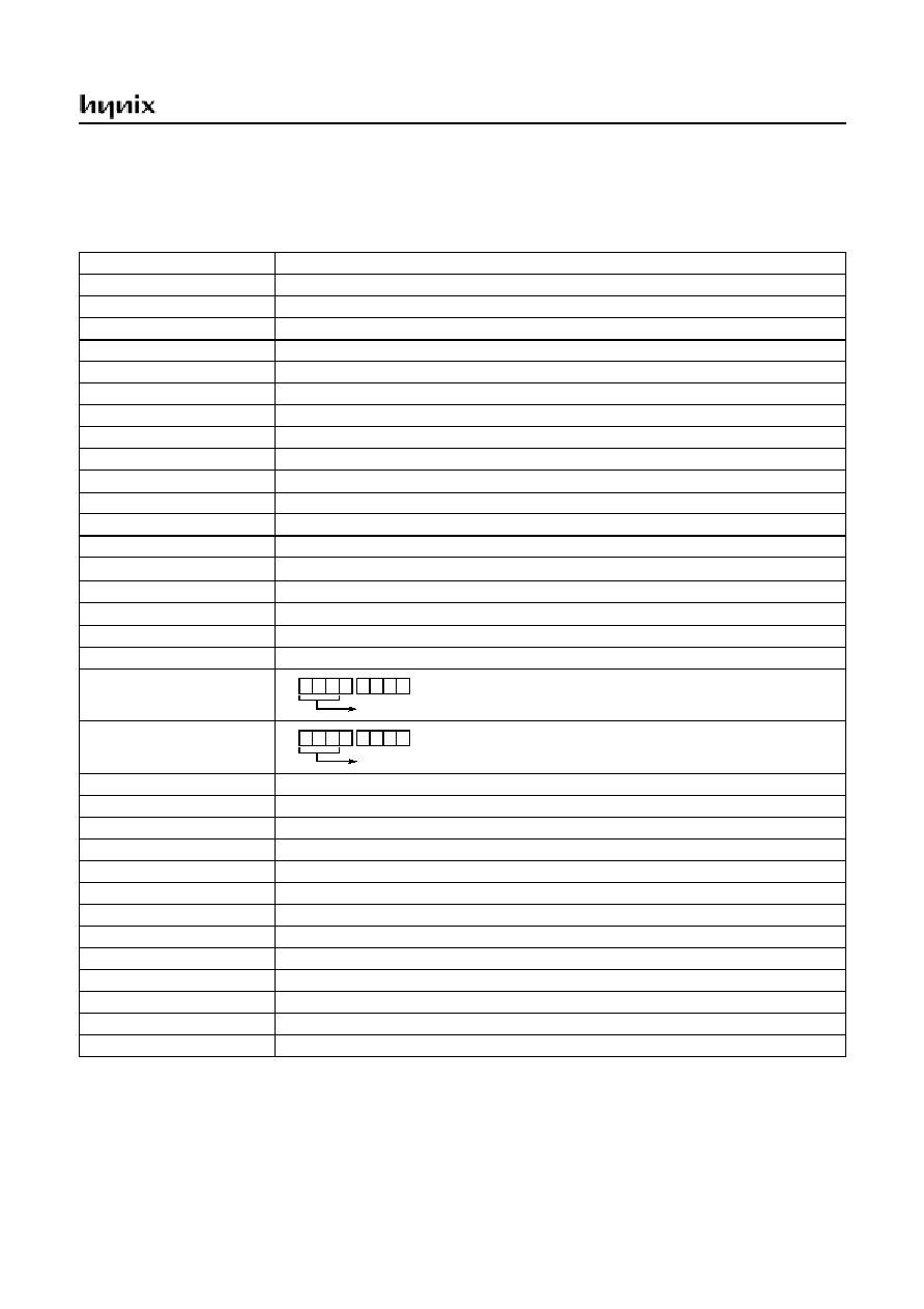
GMS81C5108 APPENDIX
JUNE 2001 Ver 1.0
iii
B. INSTRUCTION
B.1 Terminology List
Terminology
Description
A
Accumulator
X
X - register
Y
Y - register
PSW
Program Status Word
#imm
8-bit Immediate data
dp
Direct Page Offset Address
!abs
Absolute Address
[ ]
Indirect expression
{ }
Register Indirect expression
{ }+
Register Indirect expression, after that, Register auto-increment
.bit
Bit Position
A.bit
Bit Position of Accumulator
dp.bit
Bit Position of Direct Page Memory
M.bit
Bit Position of Memory Data (000
H
~0FFF
H
)
rel
Relative Addressing Data
upage
U-page (0FF00
H
~0FFFF
H
) Offset Address
n
Table CALL Number (0~15)
+
Addition
x
Upper Nibble Expression in Opcode
y
Upper Nibble Expression in Opcode
-
Subtraction
×
Multiplication
/
Division
( )
Contents Expression
AND
OR
Exclusive OR
~
NOT
Assignment / Transfer / Shift Left
Shift Right
Exchange
=
Equal
Not Equal
0
Bit Position
1
Bit Position
GMS81C5108 APPENDIX
iv
JUNE 2001 Ver 1.0
B.2 Instruction Map
LOW
HIGH
00000
00
00001
01
00010
02
00011
03
00100
04
00101
05
00110
06
00111
07
01000
08
01001
09
01010
0A
01011
0B
01100
0C
01101
0D
01110
0E
01111
0F
000
-
SET1
dp.bit
BBS
A.bit,rel
BBS
dp.bit,rel
ADC
#imm
ADC
dp
ADC
dp+X
ADC
!abs
ASL
A
ASL
dp
TCALL
0
SETA1
.bit
BIT
dp
POP
A
PUSH
A
BRK
001
CLRC
SBC
#imm
SBC
dp
SBC
dp+X
SBC
!abs
ROL
A
ROL
dp
TCALL
2
CLRA1
.bit
COM
dp
POP
X
PUSH
X
BRA
rel
010
CLRG
CMP
#imm
CMP
dp
CMP
dp+X
CMP
!abs
LSR
A
LSR
dp
TCALL
4
NOT1
M.bit
TST
dp
POP
Y
PUSH
Y
PCALL
Upage
011
DI
OR
#imm
OR
dp
OR
dp+X
OR
!abs
ROR
A
ROR
dp
TCALL
6
OR1
OR1B
CMPX
dp
POP
PSW
PUSH
PSW
RET
100
CLRV
AND
#imm
AND
dp
AND
dp+X
AND
!abs
INC
A
INC
dp
TCALL
8
AND1
AND1B
CMPY
dp
CBNE
dp+X
TXSP
INC
X
101
SETC
EOR
#imm
EOR
dp
EOR
dp+X
EOR
!abs
DEC
A
DEC
dp
TCALL
10
EOR1
EOR1B
DBNE
dp
XMA
dp+X
TSPX
DEC
X
110
SETG
LDA
#imm
LDA
dp
LDA
dp+X
LDA
!abs
TXA
LDY
dp
TCALL
12
LDC
LDCB
LDX
dp
LDX
dp+Y
XCN
DAS
111
EI
LDM
dp,#imm
STA
dp
STA
dp+X
STA
!abs
TAX
STY
dp
TCALL
14
STC
M.bit
STX
dp
STX
dp+Y
XAX
STOP
LOW
HIGH
10000
10
10001
11
10010
12
10011
13
10100
14
10101
15
10110
16
10111
17
11000
18
11001
19
11010
1A
11011
1B
11100
1C
11101
1D
11110
1E
11111
1F
000
BPL
rel
CLR1
dp.bit
BBC
A.bit,rel
BBC
dp.bit,rel
ADC
{X}
ADC
!abs+Y
ADC
[dp+X]
ADC
[dp]+Y
ASL
!abs
ASL
dp+X
TCALL
1
JMP
!abs
BIT
!abs
ADDW
dp
LDX
#imm
JMP
[!abs]
001
BVC
rel
SBC
{X}
SBC
!abs+Y
SBC
[dp+X]
SBC
[dp]+Y
ROL
!abs
ROL
dp+X
TCALL
3
CALL
!abs
TEST
!abs
SUBW
dp
LDY
#imm
JMP
[dp]
010
BCC
rel
CMP
{X}
CMP
!abs+Y
CMP
[dp+X]
CMP
[dp]+Y
LSR
!abs
LSR
dp+X
TCALL
5
MUL
TCLR1
!abs
CMPW
dp
CMPX
#imm
CALL
[dp]
011
BNE
rel
OR
{X}
OR
!abs+Y
OR
[dp+X]
OR
[dp]+Y
ROR
!abs
ROR
dp+X
TCALL
7
DBNE
Y
CMPX
!abs
LDYA
dp
CMPY
#imm
RETI
100
BMI
rel
AND
{X}
AND
!abs+Y
AND
[dp+X]
AND
[dp]+Y
INC
!abs
INC
dp+X
TCALL
9
DIV
CMPY
!abs
INCW
dp
INC
Y
TAY
101
BVS
rel
EOR
{X}
EOR
!abs+Y
EOR
[dp+X]
EOR
[dp]+Y
DEC
!abs
DEC
dp+X
TCALL
11
XMA
{X}
XMA
dp
DECW
dp
DEC
Y
TYA
110
BCS
rel
LDA
{X}
LDA
!abs+Y
LDA
[dp+X]
LDA
[dp]+Y
LDY
!abs
LDY
dp+X
TCALL
13
LDA
{X}+
LDX
!abs
STYA
dp
XAY
DAA
111
BEQ
rel
STA
{X}
STA
!abs+Y
STA
[dp+X]
STA
[dp]+Y
STY
!abs
STY
dp+X
TCALL
15
STA
{X}+
STX
!abs
CBNE
dp
XYX
NOP
GMS81C5108 APPENDIX
JUNE 2001 Ver 1.0
v
B.3 Instruction Set
Arithmetic / Logic Operation
No.
Mnemonic
Op
Code
Byte
No
Cycle
No
Operation
Flag
NVGBHIZC
1
ADC #imm
04
2
2
Add with carry.
2
ADC dp
05
2
3
A
( A ) + ( M ) + C
3
ADC dp + X
06
2
4
4
ADC !abs
07
3
4
NV--H-ZC
5
ADC !abs + Y
15
3
5
6
ADC [ dp + X ]
16
2
6
7
ADC [ dp ] + Y
17
2
6
8
ADC { X }
14
1
3
9
AND #imm
84
2
2
Logical AND
10
AND dp
85
2
3
A
( A )
( M )
11
AND dp + X
86
2
4
12
AND !abs
87
3
4
N-----Z-
13
AND !abs + Y
95
3
5
14
AND [ dp + X ]
96
2
6
15
AND [ dp ] + Y
97
2
6
16
AND { X }
94
1
3
17
ASL A
08
1
2
Arithmetic shift left
18
ASL dp
09
2
4
N-----ZC
19
ASL dp + X
19
2
5
20
ASL !abs
18
3
5
21
CMP #imm
44
2
2
Compare accumulator contents with memory contents
( A ) - ( M )
22
CMP dp
45
2
3
23
CMP dp + X
46
2
4
24
CMP !abs
47
3
4
N-----ZC
25
CMP !abs + Y
55
3
5
26
CMP [ dp + X ]
56
2
6
27
CMP [ dp ] + Y
57
2
6
28
CMP { X }
54
1
3
29
CMPX #imm
5E
2
2
Compare X contents with memory contents
30
CMPX dp
6C
2
3
( X ) - ( M )
N-----ZC
31
CMPX !abs
7C
3
4
32
CMPY #imm
7E
2
2
Compare Y contents with memory contents
33
CMPY dp
8C
2
3
( Y ) - ( M )
N-----ZC
34
CMPY !abs
9C
3
4
35
COM dp
2C
2
4
1'S Complement : ( dp )
~( dp )
N-----Z-
36
DAA
DF
1
3
Decimal adjust for addition
N-----ZC
37
DAS
CF
1
3
Decimal adjust for subtraction
N-----ZC
38
DEC A
A8
1
2
Decrement
N-----Z-
39
DEC dp
A9
2
4
M
( M ) - 1
N-----Z-
40
DEC dp + X
B9
2
5
N-----Z-
41
DEC !abs
B8
3
5
N-----Z-
42
DEC X
AF
1
2
N-----Z-
43
DEC Y
BE
1
2
N-----Z-
7 6 5 4 3 2 1 0
"0"
C
GMS81C5108 APPENDIX
vi
JUNE 2001 Ver 1.0
44
DIV
9B
1
12
Divide : YA / X Q: A, R: Y
NV--H-Z-
45
EOR #imm
A4
2
2
Exclusive OR
46
EOR dp
A5
2
3
A
( A )
( M )
47
EOR dp + X
A6
2
4
48
EOR !abs
A7
3
4
N-----Z-
49
EOR !abs + Y
B5
3
5
50
EOR [ dp + X ]
B6
2
6
51
EOR [ dp ] + Y
B7
2
6
52
EOR { X }
B4
1
3
53
INC A
88
1
2
Increment
N-----ZC
54
INC dp
89
2
4
M
( M ) + 1
N-----Z-
55
INC dp + X
99
2
5
N-----Z-
56
INC !abs
98
3
5
N-----Z-
57
INC X
8F
1
2
N-----Z-
58
INC Y
9E
1
2
N-----Z-
59
LSR A
48
1
2
Logical shift right
60
LSR dp
49
2
4
N-----ZC
61
LSR dp + X
59
2
5
62
LSR !abs
58
3
5
63
MUL
5B
1
9
Multiply : YA
Y
×
A
N-----Z-
64
OR #imm
64
2
2
Logical OR
65
OR dp
65
2
3
A
( A )
( M )
66
OR dp + X
66
2
4
67
OR !abs
67
3
4
N-----Z-
68
OR !abs + Y
75
3
5
69
OR [ dp + X ]
76
2
6
70
OR [ dp ] + Y
77
2
6
71
OR { X }
74
1
3
72
ROL A
28
1
2
Rotate left through Carry
73
ROL dp
29
2
4
N-----ZC
74
ROL dp + X
39
2
5
75
ROL !abs
38
3
5
76
ROR A
68
1
2
Rotate right through Carry
77
ROR dp
69
2
4
N-----ZC
78
ROR dp + X
79
2
5
79
ROR !abs
78
3
5
80
SBC #imm
24
2
2
Subtract with Carry
81
SBC dp
25
2
3
A
( A ) - ( M ) - ~( C )
82
SBC dp + X
26
2
4
83
SBC !abs
27
3
4
NV--HZC
84
SBC !abs + Y
35
3
5
85
SBC [ dp + X ]
36
2
6
86
SBC [ dp ] + Y
37
2
6
87
SBC { X }
34
1
3
88
TST dp
4C
2
3
Test memory contents for negative or zero, ( dp ) - 00
H
N-----Z-
89
XCN
CE
1
5
Exchange nibbles within the accumulator
A
7
~A
4
A
3
~A
0
N-----Z-
No.
Mnemonic
Op
Code
Byte
No
Cycle
No
Operation
Flag
NVGBHIZC
7 6 5 4 3 2 1 0
"0"
C
7 6 5 4 3 2 1 0
C
7 6 5 4 3 2 1 0
C
GMS81C5108 APPENDIX
JUNE 2001 Ver 1.0
vii
Register / Memory Operation
No.
Mnemonic
Op
Code
Byte
No
Cycle
No
Operation
Flag
NVGBHIZC
1
LDA #imm
C4
2
2
Load accumulator
2
LDA dp
C5
2
3
A
( M )
3
LDA dp + X
C6
2
4
4
LDA !abs
C7
3
4
5
LDA !abs + Y
D5
3
5
N-----Z-
6
LDA [ dp + X ]
D6
2
6
7
LDA [ dp ] + Y
D7
2
6
8
LDA { X }
D4
1
3
9
LDA { X }+
DB
1
4
X- register auto-increment : A
( M ) , X
X + 1
10
LDM dp,#imm
E4
3
5
Load memory with immediate data : ( M )
imm
--------
11
LDX #imm
1E
2
2
Load X-register
12
LDX dp
CC
2
3
X
( M )
N-----Z-
13
LDX dp + Y
CD
2
4
14
LDX !abs
DC
3
4
15
LDY #imm
3E
2
2
Load Y-register
16
LDY dp
C9
2
3
Y
( M )
N-----Z-
17
LDY dp + X
D9
2
4
18
LDY !abs
D8
3
4
19
STA dp
E5
2
4
Store accumulator contents in memory
20
STA dp + X
E6
2
5
( M )
A
21
STA !abs
E7
3
5
22
STA !abs + Y
F5
3
6
--------
23
STA [ dp + X ]
F6
2
7
24
STA [ dp ] + Y
F7
2
7
25
STA { X }
F4
1
4
26
STA { X }+
FB
1
4
X- register auto-increment : ( M )
A, X
X + 1
27
STX dp
EC
2
4
Store X-register contents in memory
28
STX dp + Y
ED
2
5
( M )
X
--------
29
STX !abs
FC
3
5
30
STY dp
E9
2
4
Store Y-register contents in memory
31
STY dp + X
F9
2
5
( M )
Y
--------
32
STY !abs
F8
3
5
33
TAX
E8
1
2
Transfer accumulator contents to X-register : X
A
N-----Z-
34
TAY
9F
1
2
Transfer accumulator contents to Y-register : Y
A
N-----Z-
35
TSPX
AE
1
2
Transfer stack-pointer contents to X-register : X
sp
N-----Z-
36
TXA
C8
1
2
Transfer X-register contents to accumulator: A
X
N-----Z-
37
TXSP
8E
1
2
Transfer X-register contents to stack-pointer: sp
X
N-----Z-
38
TYA
BF
1
2
Transfer Y-register contents to accumulator: A
Y
N-----Z-
39
XAX
EE
1
4
Exchange X-register contents with accumulator :X
A
--------
40
XAY
DE
1
4
Exchange Y-register contents with accumulator :Y
A
--------
41
XMA dp
BC
2
5
Exchange memory contents with accumulator
42
XMA dp+X
AD
2
6
( M )
A
N-----Z-
43
XMA {X}
BB
1
5
44
XYX
FE
1
4
Exchange X-register contents with Y-register : X
Y
--------
GMS81C5108 APPENDIX
viii
JUNE 2001 Ver 1.0
16-BIT operation
Bit Manipulation
No.
Mnemonic
Op
Code
Byte
No
Cycle
No
Operation
Flag
NVGBHIZC
1
ADDW dp
1D
2
5
16-Bits add without Carry
YA
( YA ) + ( dp +1 ) ( dp )
NV--H-ZC
2
CMPW dp
5D
2
4
Compare YA contents with memory pair contents :
(YA)
-
(dp+1)(dp)
N-----ZC
3
DECW dp
BD
2
6
Decrement memory pair
( dp+1)( dp)
( dp+1) ( dp) - 1
N-----Z-
4
INCW dp
9D
2
6
Increment memory pair
( dp+1) ( dp)
( dp+1) ( dp ) + 1
N-----Z-
5
LDYA dp
7D
2
5
Load YA
YA
( dp +1 ) ( dp )
N-----Z-
6
STYA dp
DD
2
5
Store YA
( dp +1 ) ( dp )
YA
--------
7
SUBW dp
3D
2
5
16-Bits subtract without carry
YA
( YA ) - ( dp +1) ( dp)
NV--H-ZC
No.
Mnemonic
Op
Code
Byte
No
Cycle
No
Operation
Flag
NVGBHIZC
1
AND1 M.bit
8B
3
4
Bit AND C-flag : C
( C )
( M .bit )
-------C
2
AND1B M.bit
8B
3
4
Bit AND C-flag and NOT : C
( C )
~( M .bit )
-------C
3
BIT dp
0C
2
4
Bit test A with memory :
MM----Z-
4
BIT !abs
1C
3
5
Z
( A )
( M ) , N
( M
7
) , V
( M
6
)
5
CLR1 dp.bit
y1
2
4
Clear bit : ( M.bit )
"0"
--------
6
CLRA1 A.bit
2B
2
2
Clear A bit : ( A.bit )
"0"
--------
7
CLRC
20
1
2
Clear C-flag : C
"0"
-------0
8
CLRG
40
1
2
Clear G-flag : G
"0"
--0-----
9
CLRV
80
1
2
Clear V-flag : V
"0"
-0--0---
10
EOR1 M.bit
AB
3
5
Bit exclusive-OR C-flag : C
( C )
( M .bit )
-------C
11
EOR1B M.bit
AB
3
5
Bit exclusive-OR C-flag and NOT : C
( C )
~(M .bit)
-------C
12
LDC M.bit
CB
3
4
Load C-flag : C
( M .bit )
-------C
13
LDCB M.bit
CB
3
4
Load C-flag with NOT : C
~( M .bit )
-------C
14
NOT1 M.bit
4B
3
5
Bit complement : ( M .bit )
~( M .bit )
--------
15
OR1 M.bit
6B
3
5
Bit OR C-flag : C
( C )
( M .bit )
-------C
16
OR1B M.bit
6B
3
5
Bit OR C-flag and NOT : C
( C )
~( M .bit )
-------C
17
SET1 dp.bit
x1
2
4
Set bit : ( M.bit )
"1"
--------
18
SETA1 A.bit
0B
2
2
Set A bit : ( A.bit )
"1"
--------
19
SETC
A0
1
2
Set C-flag : C
"1"
-------1
20
SETG
C0
1
2
Set G-flag : G
"1"
--1-----
21
STC M.bit
EB
3
6
Store C-flag : ( M .bit )
C
--------
22
TCLR1 !abs
5C
3
6
Test and clear bits with A :
A - ( M ) , ( M )
( M )
~( A )
N-----Z-
23
TSET1 !abs
3C
3
6
Test and set bits with A :
A - ( M ) , ( M )
( M )
( A )
N-----Z-
GMS81C5108 APPENDIX
JUNE 2001 Ver 1.0
ix
Branch / Jump Operation
No.
Mnemonic
Op
Code
Byte
No
Cycle
No
Operation
Flag
NVGBHIZC
1
BBC A.bit,rel
y2
2
4/6
Branch if bit clear :
--------
2
BBC dp.bit,rel
y3
3
5/7
if ( bit ) = 0 , then pc
( pc ) + rel
3
BBS A.bit,rel
x2
2
4/6
Branch if bit set :
--------
4
BBS dp.bit,rel
x3
3
5/7
if ( bit ) = 1 , then pc
( pc ) + rel
5
BCC rel
50
2
2/4
Branch if carry bit clear
if ( C ) = 0 , then pc
( pc ) + rel
--------
6
BCS rel
D0
2
2/4
Branch if carry bit set
if ( C ) = 1 , then pc
( pc ) + rel
--------
7
BEQ rel
F0
2
2/4
Branch if equal
if ( Z ) = 1 , then pc
( pc ) + rel
--------
8
BMI rel
90
2
2/4
Branch if minus
if ( N ) = 1 , then pc
( pc ) + rel
--------
9
BNE rel
70
2
2/4
Branch if not equal
if ( Z ) = 0 , then pc
( pc ) + rel
--------
10
BPL rel
10
2
2/4
Branch if minus
if ( N ) = 0 , then pc
( pc ) + rel
--------
11
BRA rel
2F
2
4
Branch always
pc
( pc ) + rel
--------
12
BVC rel
30
2
2/4
Branch if overflow bit clear
if (V) = 0 , then pc
( pc) + rel
--------
13
BVS rel
B0
2
2/4
Branch if overflow bit set
if (V) = 1 , then pc
( pc ) + rel
--------
14
CALL !abs
3B
3
8
Subroutine call
15
CALL [dp]
5F
2
8
M( sp)
( pc
H
), sp
sp - 1, M(sp)
(pc
L
), sp
sp - 1,
if !abs, pc
abs ; if [dp], pc
L
( dp ), pc
H
( dp+1 ) .
--------
16
CBNE dp,rel
FD
3
5/7
Compare and branch if not equal :
--------
17
CBNE dp+X,rel
8D
3
6/8
if ( A )
( M ) , then pc
( pc ) + rel.
18
DBNE dp,rel
AC
3
5/7
Decrement and branch if not equal :
--------
19
DBNE Y,rel
7B
2
4/6
if ( M )
0 , then pc
( pc ) + rel.
20
JMP !abs
1B
3
3
Unconditional jump
21
JMP [!abs]
1F
3
5
pc
jump address
--------
22
JMP [dp]
3F
2
4
23
PCALL upage
4F
2
6
U-page call
M(sp)
( pc
H
), sp
sp - 1, M(sp)
( pc
L
),
sp
sp - 1, pc
L
( upage ), pc
H
"0FF
H
" .
--------
24
TCALL n
nA
1
8
Table call : (sp)
( pc
H
), sp
sp - 1,
M(sp)
( pc
L
),sp
sp - 1,
pc
L
(Table vector L), pc
H
(Table vector H)
--------
GMS81C5108 APPENDIX
x
JUNE 2001 Ver 1.0
Control Operation & Etc.
No.
Mnemonic
Op
Code
Byte
No
Cycle
No
Operation
Flag
NVGBHIZC
1
BRK
0F
1
8
Software interrupt : B
"1", M(sp)
(pc
H
), sp
sp-1,
M(s)
(pc
L
), sp
sp - 1, M(sp)
(PSW), sp
sp -1,
pc
L
( 0FFDE
H
) , pc
H
( 0FFDF
H
) .
---1-0--
2
DI
60
1
3
Disable all interrupts : I
"0"
-----0--
3
EI
E0
1
3
Enable all interrupt : I
"1"
-----1--
4
NOP
FF
1
2
No operation
--------
5
POP A
0D
1
4
sp
sp + 1, A
M( sp )
6
POP X
2D
1
4
sp
sp + 1, X
M( sp )
--------
7
POP Y
4D
1
4
sp
sp + 1, Y
M( sp )
8
POP PSW
6D
1
4
sp
sp + 1, PSW
M( sp )
restored
9
PUSH A
0E
1
4
M( sp )
A , sp
sp - 1
10
PUSH X
2E
1
4
M( sp )
X , sp
sp - 1
--------
11
PUSH Y
4E
1
4
M( sp )
Y , sp
sp - 1
12
PUSH PSW
6E
1
4
M( sp )
PSW , sp
sp - 1
13
RET
6F
1
5
Return from subroutine
sp
sp +1, pc
L
M( sp ), sp
sp +1, pc
H
M( sp )
--------
14
RETI
7F
1
6
Return from interrupt
sp
sp +1, PSW
M( sp ), sp
sp + 1,
pc
L
M( sp ), sp
sp + 1, pc
H
M( sp )
restored
15
STOP
EF
1
3
Stop mode ( halt CPU, stop oscillator )
--------
C. MASK ORDER SHEET
MASK ORDER & VERIFICATION SHEET
GMS81C5108
1. Customer Information
Company Name
Application
Order Date
YYYY
Tel:
Fax:
Name &
Signature:
Customer should write inside thick line box.
2. Device Information
MM
DD
3. Marking Specification
4. Delivery Schedule
Date
Quantity
HYNIX Confirmation
YYYY
MM
DD
YYYY
MM
DD
Customer sample
Risk order
pcs
pcs
E-mail address:
5. ROM Code Verification
YYYY
MM
DD
Verification date:
Please confirm out verification data.
Check sum:
Tel:
Fax:
Name &
Signature:
E-mail address:
YYYY
MM
DD
Approval date:
I agree with your verification data and confirm you to
make mask set.
Tel:
Fax:
Name &
Signature:
E-mail address:
- UD
FE
B
. 2001
G M S81C 5108-U D
YYW W KO R EA
Package
80QFP
Set "00" in
this area
0000
H
E000
H
FFFF
H
.OTP file data
DFFF
H
M
a
sk Da
ta
Hitel
Chollian
Internet
File Name : ( .OTP)
Check Sum : ( )
OSC Option
Crystal
R
Reset Pull Up
YES
NO
8K
ROM Size
G M S81C 5108-U D
YYW W KO R EA
C ustom er's Area
If the customer logo & part number must be used in this area,
(Please check mark into )
please submit a clean original logo & part number.
Hynix Sem iconductor Inc.
Document Outline