HC2510C
1
HC2510C
Features
l
Phase-Locked Loop Clock Distribution for
Synchronous DRAM Applications
l
Supports PC-100 and Meets "PC100 SDRAM
registered DIMM Specification Rev. 1.2"
l
Distributes One Clock Input to One Bank of Ten
Outputs
l
No External RC Network Required
l
External Feedback (FBIN) Pin is Used to
Synchronize the Outputs to the Clock Input
l
Separate Output Enable for Each Output Bank
l
Operates at 3.3 V V
cc
l
125 MHz Maximum Frequency
l
On-chip Series Damping Resistors
l
Support Spread Spectrum Clock(SSC)
Synthesizers
l
ESD Protection Exceeds 3000 V per MIL-STD-
883, Method 3015 ; Exceeds 350 V Using
Machine Model ( C = 200 pF, R = 0 )
l
Latch-Up Performance Exceeds 400 mA per
JESD 17
l
Packaged in Plastic 24-Pin Thin Shrink Small-
Outline Package
Pin Configuration
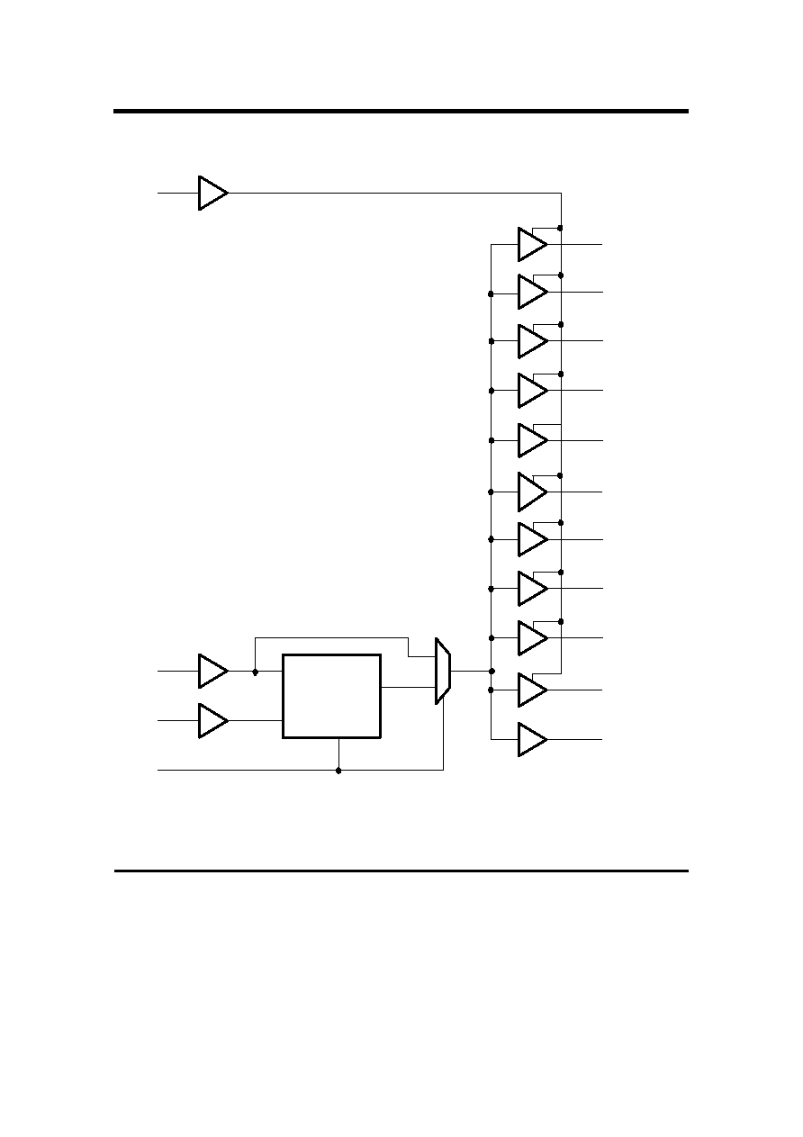
General Description
The HC2510C is a
low-skew, low jitter, phase-
locked loop(PLL) clock driver, distributing high
frequency clock signals for SDRAM.
The HC2510C operates at 3.3V V
cc
and provides
integrated series-damping resistors that make it ideal
for driving point-to-point loads. The propagation delay
from the CLK input to any clock output is nearly zero.
Ten outputs provide low-skew and low-jitter clocks.
All outputs can be enabled or disabled via the control
input(G). Output signal duty cycles are adjusted to 50
percent, independent of the duty cycle at CLK.
The HC2510C is specially designed to interface with
high speed SDRAM applications in the range of
25MHz to 125MHz and includes an internal RC
network which provides excellent jitter characteristics
and eliminates the needs for external components.
For the test purpose, the PLL can be bypassed by
strapping AV
cc
to ground.
The HC2510C is characterized for operation from 0
∞
C
to 85
∞
C.
Function Table
INPUTS
OUTPUTS
1Y
G CLK
(0:9)
FBOUT
X
L
L
L
L
H
L
H
H
H
H
H
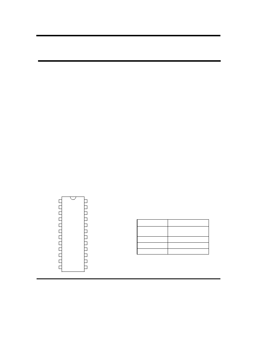
TSSOP 24 PACKAGE
(TOP VIEW)
AGND
Vcc
1Y0
1Y1
1Y2
GND
GND
1Y3
1Y4
Vcc
G
FBOUT
CLK
AVcc
Vcc
1Y9
1Y8
GND
GND
1Y7
1Y6
1Y5
Vcc
FBIN
1
2
3
4
5
6
7
8
9
10
11
12
24
23
22
21
20
19
18
17
16
15
14
13
HC2510C
3
Table 1. Pin Description
Pin Name
Pin No.
Type
Functional Description
CLK
24
I
Clock Input. CLK provides the reference signal to the internal
PLL.
FBIN
13
I
Feedback Input. FBIN provides the feedback signal to the
internal PLL.
G
11
I
Output Bank Enable. When G is high, all outputs 1Y(0:9) are
enabled.
When G is low, Outputs 1Y(0:9) are disable to a logic-low
state.
FBOUT
12
O
Feedback Output. FBOUT completes the feedback loop of the
PLL by being wired to FBIN.
1Y(0:9)
3,4,5,8,9
15,16,17,20,2
1
O
Clock Outputs. These outputs provide low-skew copies of
CLKIN. Each output has an embedded series-damping
resistor.
AV
cc
23
Power
Analog Power Supply. AV
cc
provides the power reference for
the analog circuitry. AV
cc
can be also used to bypass the PLL
for the test purpose. When AV
cc
is strapped to ground, PLL is
bypassed and CLK is buffered directly to the device outputs.
AGND
1
Groun
d
Analog Ground. AGND provides the ground reference for the
analog circuitry.
V
cc
2,10,14,22
Power Power Supply
GND
6,7,18,19
Groun
d
Ground
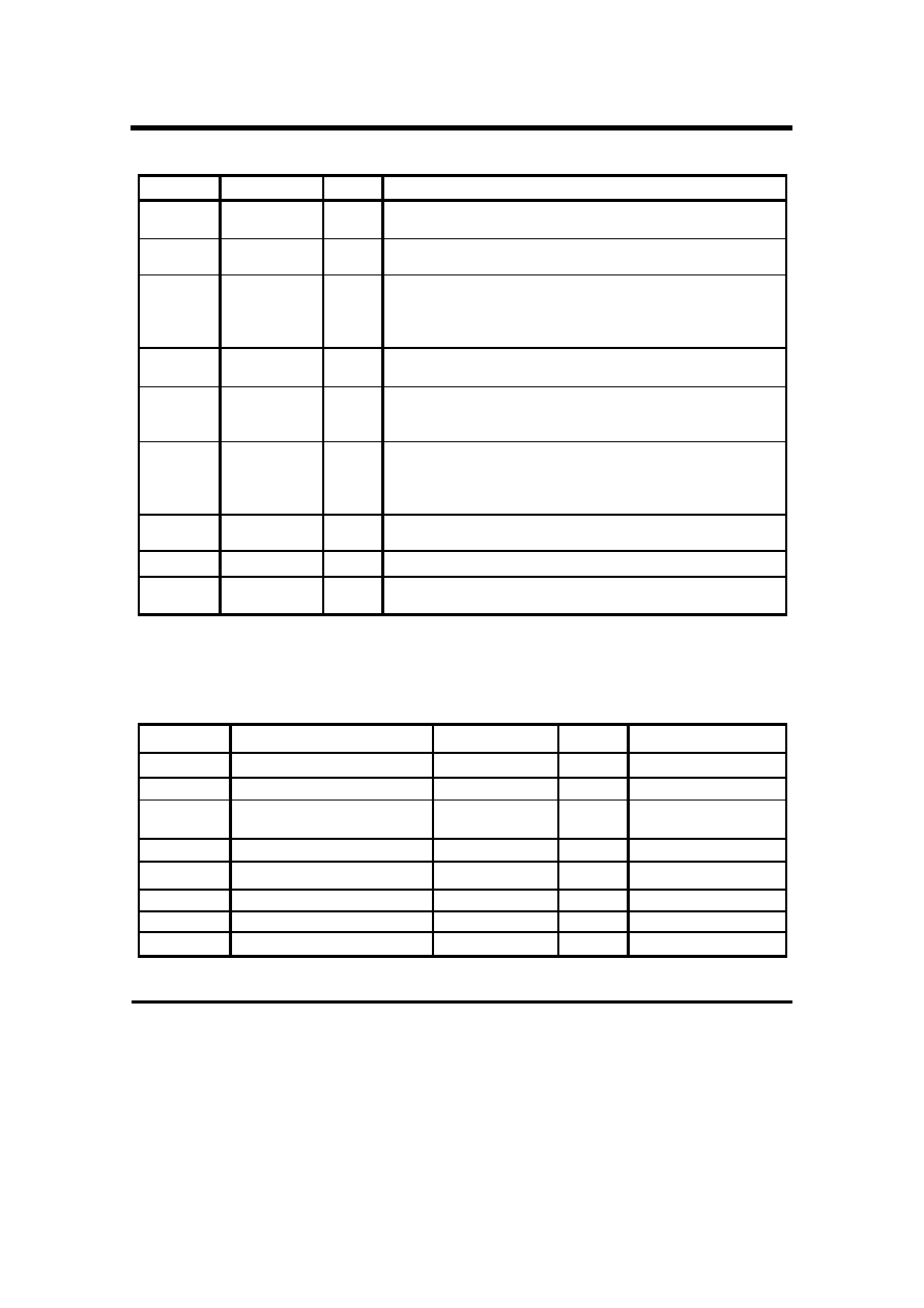
Table 2. Absolute Maximum Ratings Over Operating Free-air
Temperature Range
Symbols
Parameter
Value
Unit
Conditions
V
cc
Supply Voltage Range
-0.5 to 4.6
V
V
I
Input Voltage Range
-0.5 to 6.5
V
V
o
Voltage Range applied to any
input in the high or low state
-0.5 to Vcc+0.5
V
I
IK
Input Clamp Current
±
50
mA
V
I
<0 or V
I
>V
cc
I
OK
Output Clamp Current
±
50
mA
V
o
<0 or V
o
>V
cc
I
o
Continuous Output Current
±
50
mA
V
o
=0 to V
cc
P
MAX
Maximum Power Dissipaiton
0.7
W
T
stg
Storage Temperature Range
- 65 to 150
∞
C
HC2510C
4
Table 3. Recommended Operating Conditions
Value
Symbol
Parameter
Min
Max
Unit
Condition
AV
CC
Supply Voltage
3
3.6
V
V
IH
High-level Input Voltage
2
V
V
IL
Low-level Input Voltage
0.8
V
V
I
Input Voltage
0
V
CC
V
I
OH
High-level Output Current
-12
mA
I
OL
Low-level Output Current
12
mA
T
A
Operating Free-air Temperature
0
85
∞
C
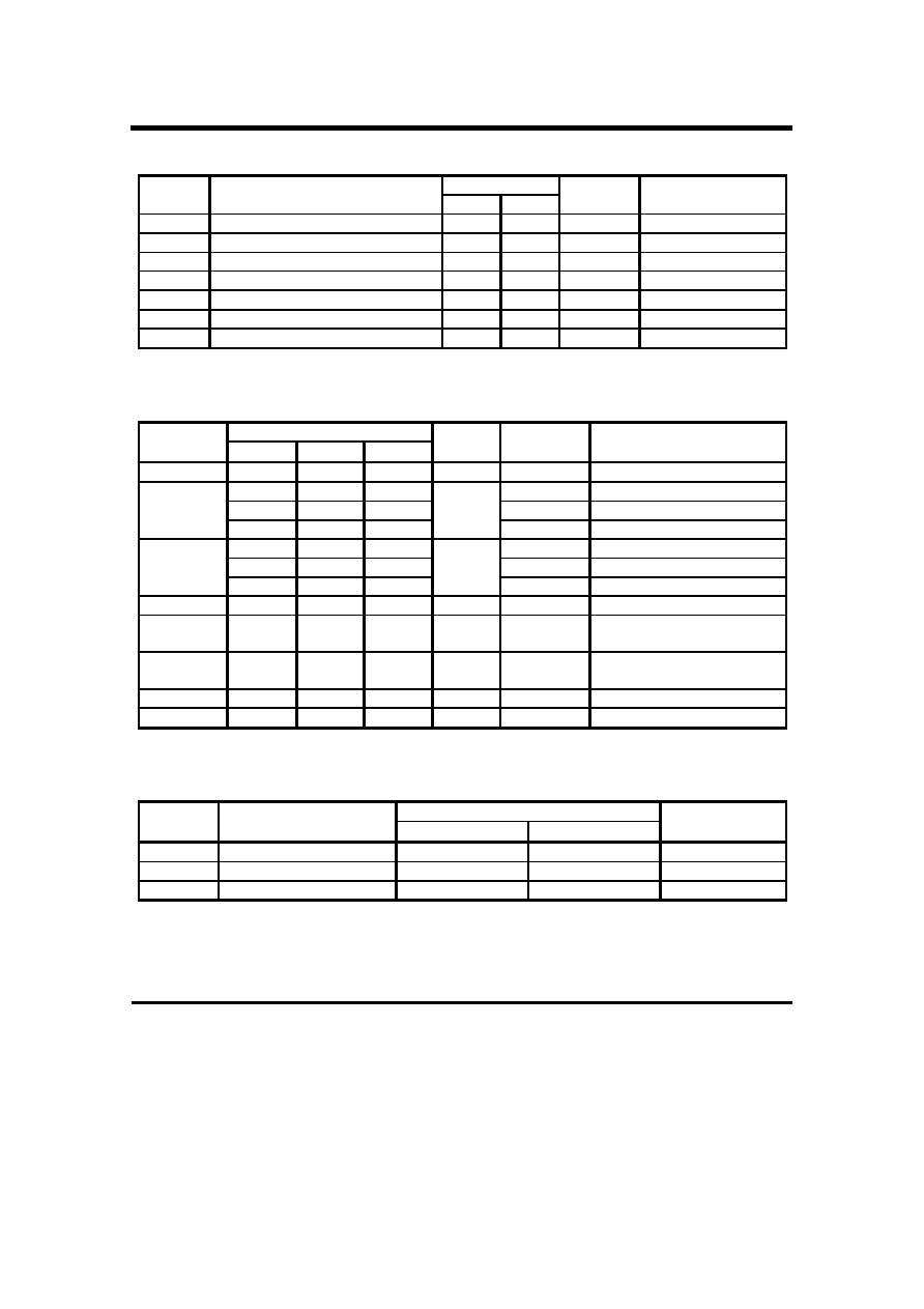
Table 4. Electrical Characteristics Over Recommended Operating Free-air
Temperature Range
Value
Symbol
Min
Typ
Max
Unit
AV
CC
(V)
Test Conditions
V
IK
-1.2
V
3
I
I
= -18mA
Vcc-0.2
Min to Max
I
OH
= -100
µ
A
2.1
3
I
OH
= -12 mA
V
OH
2.4
V
3
I
OH
= -6 mA
0.2
Min to Max
I
OL
=100 mA
0.8
3
I
OL
= 12 mA
V
OL
0.55
V
3
I
OL
= 6 mA
I
I
±
5
µ
A
3.6
V
I
=V
CC
or GND
I
CC
10
µ
A
3.6
V
I
=V
CC
or GND, I
O
= 0,
Ouputs: low or high
I
CC
500
µ
A
3.3 to 3.6
One input at V
CC
- 0.6V,
Other Inputs at V
CC
or GND
C
i
4
pF
3.3
V
I
= V
CC
or GND
C
o
6
pF
3.3
V
O
= V
CC
or GND
Table 5.Timing Requirements Over Recommended Ranges of Supply Voltage
and Operating free-air Temperature
Value
Symbol
Parameter
Min
Max
Unit
f
clock
Clock Frequency
25
125
MHz
Input Clock Duty Cycle
40
60
%
Stabilization Time
1
ms
Time to obtain phase lock of its feedback signal to its reference signal.

HC2510C
5
Table 6. Switching Characteristics Over Recommended Ranges of Supply
Voltage and Operating Free-air Temperature. (C
L
=30
pF
)
=
V
CC
= 3.3V
±
0.165V
V
CC
=
3.3V
±
0.3V
Parameter
From(Input)
TO(Output)
Min Typ Max Min Typ Max
Unit
66MHz < CLKIN
<
100MHz
FBIN
150
150
ps
t
phase error
CLKIN
= 100MHz
FBIN
-50
50
ps
t
sk
Any Y of FBOUT
Any Y or
FBOUT
200 ps
Jitter
(pk-pk)
CLKIN
>
66MHz
Any Y or
FBOUT
-100
100 ps
Duty
Cycle
CLKIN
>
66MHz
Any Y or
FBOUT
45
55
%
t
r
Any Y or
FBOUT
1.3 1.9 0.8
2.1 ns
t
f
Any Y or
FBOUT
1.7 2.5 1.2
2.7 ns
=
These parameters are not production tested.
Phase error does not include jitter.
Figure 1. Load Circuit and Voltage Waveforms
Notes: 1. All input pulses are supplied by generators having
the following characteristics: PRR
100MHz, Z
o
=50
, t
r
=1.2ns, t
f
=1.2ns
2.The outputs are measured one at a time with one
transition per measurement.
30pF
500
ߟ
From Output Under Test
Input
Output
50% V
CC
50% V
CC
3V
0V
V
OH
V
OL
tpd
0.4V
0.4V
tr
tf
2V
2V
Load Circuit For Outputs
Voltage Waveforms
Propagation Delay Times