
HY51V(S)65403HG/HGL
16M x 4Bit EDO DRAM
This document is a general product description and is subject to change without notice. Hyundai Electronics does not assume any
responsibility for use of circuits described. No patent licenses are implied.
Rev.0.1/Apr.01
DESCRIPTION
FEATURES
∑
Fast access time and cycle time
ORDERING INFORMATION
Part No
tRAC
tAA
tCAC
tRC
tHPC
HY51V(S)65403HG/HGL-45
45ns
23ns
12ns
74ns
17ns
HY51V(S)65403HG/HGL-5
50ns
25ns
13ns
84ns
20ns
HY51V(S)65403HG/HGL-6
60ns
30ns
15ns
104ns
25ns
45ns
50ns
60ns
Active
468mW
432mW
396mW
Standby
1.8mW(CMOS level Max)
0.72mW (L-version : Max)
Part Number
Access Time
Package
HY51V(S)65403HG/HG(L)J-45
HY51V(S)65403HG/HG(L)J-5
HY51V(S)65403HG/HG(L)J-6
45ns
50ns
60ns
400mil 32pin SOJ
HY51V(S)65403HG/HG(L)T-45
HY51V(S)65403HG/HG(L)T-5
HY51V(S)65403HG/HG(L)T-6
45ns
50ns
60ns
400mil 32pin TSOP-II
PRELIMINARY
This familiy is a 64Mbit dynamic RAM organized 16,777,216 x 4 bit configuration with Extended Data Out
mode CMOS DRAMs. Extended data out mode is a kind of page mode which is useful for the read opera-
tion. The advanced circuit and process allow this device to achieve high performance and low power dissi-
pation. features are access time(45ns or 50ns) and refresh cycle(4K ref ) and power consumption (Normal
or low power with self refresh).
Advanced CMOS process as well as circuit techniques for wide operating margins allow this device to
achieve high speed access and high reliability
∑
Extended data out operation
∑
Read-modify-write capability
∑
Multi-bit parallel test capability
∑
LVTTL(3.3V) compatible inputs and outputs
∑
/RAS only, CAS-before-/RAS, Hidden and self
refresh(L-version) capability
∑
JEDEC standard pinout
32pin plastic SOJ/TSOP-II(400mil)
∑
Single power supply of 3.3V +/- 10%
∑
Battery back up operation(L-version)
∑
Power dissipation
∑
Refresh cycle
Part No
Ref
Normal
L-part
HY51V65403HG*
4K
64ms
HY51V65403HGL*
4K
128ms
* /RAS only Refresh, CBR & Hidden Refresh
(S) : Self refresh, (L) : Low power
HY51V(S)65403HG/HGL
Rev.0.1/Apr.01
2
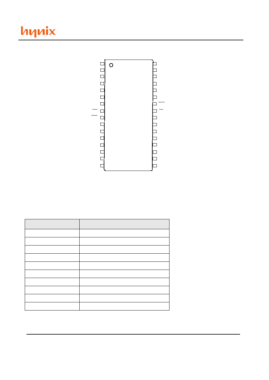
PIN CONFIGURATION
Pin
Function
/RAS
Row Address Strobe
/CAS
Column Address Strobe
/WE
Write Enable
/OE
Output Enable
A0-A11
Address Inputs
A0-A11
Refresh Address Inputs
I/O 0- I/O 3
Data Input / Output
Vcc
Power (3.3V)
Vss
Ground
NC
No connection
PIN DESCRIPTION
NC
1
2
3
4
5
6
7
8
9
10
11
12
13
14
15
16
V
CC
I/O0
I/O1
NC
NC
V
CC
WE
RAS
A0
A1
A2
A3
A4
A5
V
CC
32
17
18
19
20
21
22
23
24
25
26
27
28
29
30
31
V
SS
A6
A7
A8
A9
A10
A11
A12
OE
CAS
V
SS
I/O2
I/O3
V
SS
NC
NC
32 Pin Plastic SOJ / TSOP-II

HY51V(S)65403HG/HGL
Rev.0.1/Apr.01
3
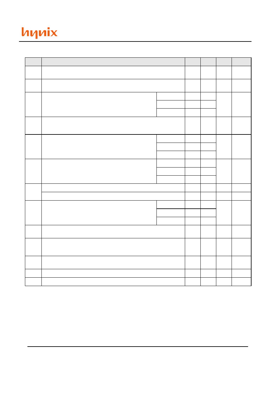
ABSOLUTE MAXIMUM RATINGS
Note : Operation at above absolute maximum rating can adversely affect device reliability.
Recommended DC OPERATING CONDITIONS
(TA=0 to 70
o
C)
Note : All voltages are referenced to Vss
1. 6.0V at pulse width 10ns which is measured at Vcc
2. -0.1V at pulse width 10ns which is measured at Vss
Parameter
Symbol
Rating
Unit
Ambient Temperature
T
A
0 ~ 70
o
C
Storage Temperature
T
STG
-55 ~ 125
o
C
Voltage on Any Pin relative to V
ss
V
T
-0.5 ~ Vcc + 0.5
(Max 4.6V)
V
Voltage on V
cc
relative to V
ss
V
cc
-0.5 ~ 4.6
V
Short Circuit Output Current
I
OUT
50
mA
Power Dissipation
P
T
1
W
Parameter
Symbol
Min
Typ.
Max
Unit
Note
Power Supply Voltage
V
cc
3.0
3.3
3.6
V
1,2
Power Supply Voltage
V
ss
0
0
0
V
2
Input High Voltage
V
IH
2.0
-
V
cc
+ 0.3
V
1
Input Low Voltage
V
IL
-0.3
-
0.8
V
1
HY51V(S)65403HG/HGL
Rev.0.1/Apr.01
4
DC CHARACTERISTICS
(Vcc = 3.3V +/- 10%, TA=0 to 70
∞
C
)
Note :
1. Icc depends on output load condition when the device is selected, Icc(max) is specified at the output open condition
2. Address can be changed once or less while RAS=VIL
3. Measured with one sequential address change per EDO cycle, tHPC
4. VIH>=Vcc-0.2V, 0V<=VIL<=0.2V
5. L-Version
Symbol
Parameter
Min
Max
Unit
Note
VOH
Output Level
Output Level voltage(Iout= -2mA)
2.4
Vcc
V
VOL
Output Level
Output Level voltage(Iout=2mA)
0
0.4
V
ICC1
Operating current ( tRC = tRC min)
45ns
-
130
mA
1, 2
50ns
-
120
60ns
-
110
I
CC2
Standby current (TTL interface)
Power supply standby current
(/RAS, /UCAS,/LCAS=VIH, Dout = High-Z)
-
1
mA
ICC3
/RAS only refresh current (tRC= tRC min)
45ns
-
130
mA
2
50ns
-
120
60ns
-
110
ICC4
Extended data out page mode current
(/RAS=VIL, /CAS, Address cycling : tHPC=tHPC min)
45ns
-
100
mA
1, 3
50ns
-
90
60ns
-
80
ICC5
CMOS interface ( /RAS, /UCAS, /LCAS >= Vcc-0.2V, Dout = High-Z)
-
0.5
mA
Standby current ( L-version)
-
200
uA
4
ICC6
/CAS-before-/RAS refresh current (tRC=tRC min)
45ns
-
130
mA
50ns
-
120
60ns
-
110
ICC7
Battery back up operating current (standby with CBR)
(tRC=31.25us, tRAS=300ns, Dout=High-Z)
-
350
uA
4, 5
ICC8
Standby current (CMOS)
Power supply standby current
/RAS=VIH, /CAS=VIL, Dout=Enable)
-
5
mA
1
ICC9
Self refresh current
(/RAS, /CAS<=0.2V, Dout=High-Z)
-
350
uA
5
II(L)
Input leakage current, Any input (0V<= Vin<=Vcc)
-5
5
uA
IO(L)
Output leakage current, (Dout is disabled, 0V<= Vout<=Vcc)
-5
5
uA
HY51V(S)65403HG/HGL
Rev.0.1/Apr.01
5
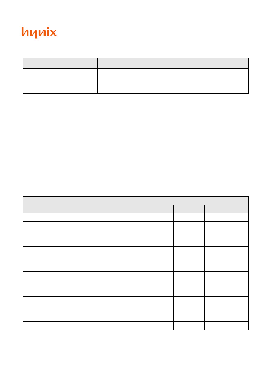
CAPACITANCE
(Vcc=3.3V +/-10%, TA=25
∞
C
)
Note : 1. Capacitance measured with Boonton Meter or effective capacitance measuring method.
2. /RAS, /UCAS and /LCAS = V
IH
to disable D
out
AC CHARACTERISTICS
(Vcc=3.3V +/-10%, TA=0~70C, Note 1, 2, 19)
Read, Write, Read-modify-Write and Refresh Cycles
Parameter
Symbol
Min.
Max
Unit
Note
Input capacitance (Address)
CI1
-
5
pF
1
Input capacitance (Clocks)
CI2
-
5
pF
1
Output capacitance (Data-in, Data-out)
CI/O
-
7
pF
1, 2
Parameter
Symbol
-45
-50
-60
Unit
Note
Min
Max
Min
Max
Min
Max
Random read or write cycle time
t
RC
74
-
84
-
104
-
ns
/RAS precharge time
t
RP
25
-
30
-
40
-
ns
/CAS precharge time
t
CP
7
-
8
-
10
-
ns
/RAS pulse width
t
RAS
45
10,000
50
10,000
60
10,000
ns
/CAS pulse width
t
CAS
7
10,000
8
10,000
10
10,000
ns
Row address set-up time
t
ASR
0
-
0
-
0
-
ns
Row address hold time
t
RAH
7
-
8
-
10
-
ns
Column address set-up time
t
ASC
0
-
0
-
0
-
ns
Column address hold time
t
CAH
7
-
8
-
10
-
ns
/RAS to /CAS delay time
t
RCD
11
33
12
37
14
45
ns
3
/RAS to Column address delay time
t
RAD
9
22
10
25
12
30
ns
4
/RAS hold time
t
RSH
12
-
13
-
15
-
ns
/CAS hold time
t
CSH
38
-
40
-
42
-
ns
/CAS to /RAS precharge time
t
CRP
5
-
5
-
5
-
ns
Test Condition
∑
Input rise and fall times = 2ns
∑
Input level : V
IL
/V
IH
= 0.0 / 0.3V
∑
Input timing reference level : V
IL
/V
IH
= 0.8/2.0V
∑
Output timing reference level :
V
OL
/V
OH
=0.8/0.2V
∑
Output load : 1 TTL gate + C
L
(100pF)
including scope and jig