HY57V283220T-I.fm
HY57V283220T-I/ HY5V22F-I
4 Banks x 1M x 32Bit Synchronous DRAM
This document is a general product description and is subject to change without notice. Hynix Semiconductor Inc. does not assume
any responsibility for use of circuits described. No patent licenses are implied.
Rev. 0.6/Nov. 02
DESCRIPTION
The Hynix HY57V283220T-I / HY5V22F-I is a 134,217,728-bit CMOS Synchronous DRAM, ideally suited for the mem-
ory applications which require wide data I/O and high bandwidth. HY57V283220T-I / HY5V22F-I is organized as
4banks of 1,048,576x32.
HY57V283220T-I / HY5V22F-I is offering fully synchronous operation referenced to a positive edge of the clock. All
inputs and outputs are synchronized with the rising edge of the clock input. The data paths are internally pipelined to
achieve very high bandwidth. All input and output voltage levels are compatible with LVTTL.
Programmable options include the length of pipeline (Read latency of 2 or 3), the number of consecutive read or write
cycles initiated by a single control command (Burst length of 1,2,4,8 or full page), and the burst count
sequence(sequential or interleave). A burst of read or write cycles in progress can be terminated by a burst terminate
command or can be interrupted and replaced by a new burst read or write command on any cycle. (This pipelined
design is not restricted by a `2N` rule.)
FEATURES
·
JEDEC standard 3.3V power supply
·
All device pins are compatible with LVTTL interface
·
86TSOP-II, 90Ball FBGA with 0.8mm of pin pitch
·
All inputs and outputs referenced to positive edge of
system clock
·
Data mask function by DQM0,1,2 and 3
·
Internal four banks operation
·
Auto refresh and self refresh
·
4096 refresh cycles / 64ms
·
Programmable Burst Length and Burst Type
- 1, 2, 4, 8 or full page for Sequential Burst
- 1, 2, 4 or 8 for Interleave Burst
·
Programmable CAS Latency ; 2, 3 Clocks
·
Burst Read Single Write operation
ORDERING INFORMATION
Part No.
Clock Frequency
Organization
Interface
Package
HY57V283220(L)T-5I
HY5V22(L)F-5I
200MHz
4Banks x 1Mbits
x32
LVTTL
86TSOP-II
90Ball FBGA
HY57V283220(L)T-55I
HY5V22(L)F-55I
183MHz
4Banks x 1Mbits
x32
LVTTL
86TSOP-II
90Ball FBGA
HY57V283220(L)T-6I
HY5V22(L)F-6I
166MHz
4Banks x 1Mbits
x32
LVTTL
86TSOP-II
90Ball FBGA
HY57V283220(L)T-7I
HY5V22(L)F-7I
143MHz
4Banks x 1Mbits
x32
LVTTL
86TSOP-II
90Ball FBGA
HY57V283220(L)T-8I
HY5V22(L)F-8I
125MHz
4Banks x 1Mbits
x32
LVTTL
86TSOP-II
90Ball FBGA
HY57V283220(L)T-PI
HY5V22(L)F-PI
100MHz
4Banks x 1Mbits
x32
LVTTL
86TSOP-II
90Ball FBGA
HY57V283220(L)T-SI
HY5V22(L)F-SI
100MHz
4Banks x 1Mbits
x32
LVTTL
86TSOP-II
90Ball FBGA
Rev. 0.6/Nov. 02 2
HY57V283220T-I / HY5V22F-I
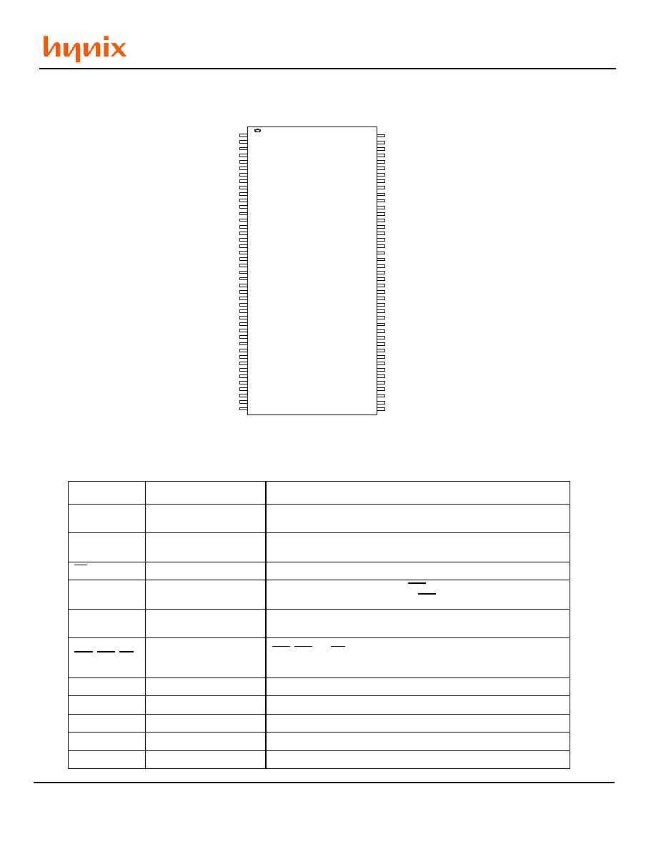
PIN CONFIGURATION ( HY57V283220T-I Series)
V
D D
D Q 0
V
D D Q
D Q 1
D Q 2
V
S S Q
D Q 3
D Q 4
V
D D Q
D Q 5
D Q 6
V
S S Q
D Q 7
N C
V
D D
D Q M 0
/W E
/C A S
/R A S
/C S
A 1 1
B A 0
B A 1
A 1 0 /A P
A 0
A 1
A 2
D Q M 2
V
D D
N C
D Q 1 6
V
S S Q
D Q 1 7
D Q 1 8
V
D D Q
D Q 1 9
D Q 2 0
V
S S Q
D Q 2 1
D Q 2 2
V
D D Q
D Q 2 3
V
D D
1
2
3
4
5
6
7
8
9
1 0
1 1
1 2
1 3
1 4
1 5
1 6
1 7
1 8
1 9
2 0
2 1
2 2
2 3
2 4
2 5
2 6
2 7
2 8
2 9
3 0
3 1
3 2
3 3
3 4
3 5
3 6
3 7
3 8
3 9
4 0
4 1
4 2
4 3
V
S S
D Q 1 5
V
S S Q
D Q 1 4
D Q 1 3
V
D D Q
D Q 1 2
D Q 1 1
V
S S Q
D Q 1 0
D Q 9
V
D D Q
D Q 8
N C
V
S S
D Q M 1
N C
N C
C L K
C K E
A 9
A 8
A 7
A 6
A 5
A 4
A 3
D Q M 3
V
S S
N C
D Q 3 1
V
D D Q
D Q 3 0
D Q 2 9
V
S S Q
D Q 2 8
D Q 2 7
V
D D Q
D Q 2 6
D Q 2 5
V
S S Q
D Q 2 4
V
S S
8 6
8 5
8 4
8 3
8 2
8 1
8 0
7 9
7 8
7 7
7 6
7 5
7 4
7 3
7 2
7 1
7 0
6 9
6 8
6 7
6 6
6 5
6 4
6 3
6 2
6 1
6 0
5 9
5 8
5 7
5 6
5 5
5 4
5 3
5 2
5 1
5 0
4 9
4 8
4 7
4 6
4 5
4 4
8 6 p in T S O P II
4 0 0 m il x 8 7 5 m il
0 .5 m m p in p it c h
V
D D
D Q 0
V
D D Q
D Q 1
D Q 2
V
S S Q
D Q 3
D Q 4
V
D D Q
D Q 5
D Q 6
V
S S Q
D Q 7
N C
V
D D
D Q M 0
/W E
/C A S
/R A S
/C S
A 1 1
B A 0
B A 1
A 1 0 /A P
A 0
A 1
A 2
D Q M 2
V
D D
N C
D Q 1 6
V
S S Q
D Q 1 7
D Q 1 8
V
D D Q
D Q 1 9
D Q 2 0
V
S S Q
D Q 2 1
D Q 2 2
V
D D Q
D Q 2 3
V
D D
1
2
3
4
5
6
7
8
9
1 0
1 1
1 2
1 3
1 4
1 5
1 6
1 7
1 8
1 9
2 0
2 1
2 2
2 3
2 4
2 5
2 6
2 7
2 8
2 9
3 0
3 1
3 2
3 3
3 4
3 5
3 6
3 7
3 8
3 9
4 0
4 1
4 2
4 3
V
S S
D Q 1 5
V
S S Q
D Q 1 4
D Q 1 3
V
D D Q
D Q 1 2
D Q 1 1
V
S S Q
D Q 1 0
D Q 9
V
D D Q
D Q 8
N C
V
S S
D Q M 1
N C
N C
C L K
C K E
A 9
A 8
A 7
A 6
A 5
A 4
A 3
D Q M 3
V
S S
N C
D Q 3 1
V
D D Q
D Q 3 0
D Q 2 9
V
S S Q
D Q 2 8
D Q 2 7
V
D D Q
D Q 2 6
D Q 2 5
V
S S Q
D Q 2 4
V
S S
8 6
8 5
8 4
8 3
8 2
8 1
8 0
7 9
7 8
7 7
7 6
7 5
7 4
7 3
7 2
7 1
7 0
6 9
6 8
6 7
6 6
6 5
6 4
6 3
6 2
6 1
6 0
5 9
5 8
5 7
5 6
5 5
5 4
5 3
5 2
5 1
5 0
4 9
4 8
4 7
4 6
4 5
V
D D
D Q 0
V
D D Q
D Q 1
D Q 2
V
S S Q
D Q 3
D Q 4
V
D D Q
D Q 5
D Q 6
V
S S Q
D Q 7
N C
V
D D
D Q M 0
/W E
/C A S
/R A S
/C S
A 1 1
B A 0
B A 1
A 1 0 /A P
A 0
A 1
A 2
D Q M 2
V
D D
N C
D Q 1 6
V
S S Q
D Q 1 7
D Q 1 8
V
D D Q
D Q 1 9
D Q 2 0
V
S S Q
D Q 2 1
D Q 2 2
V
D D Q
D Q 2 3
V
D D
1
2
3
4
5
6
7
8
9
1 0
1 1
1 2
1 3
1 4
1 5
1 6
1 7
1 8
1 9
2 0
2 1
2 2
2 3
2 4
2 5
2 6
2 7
2 8
2 9
3 0
3 1
3 2
3 3
3 4
3 5
3 6
3 7
3 8
3 9
4 0
4 1
4 2
4 3
V
S S
D Q 1 5
V
S S Q
D Q 1 4
D Q 1 3
V
D D Q
D Q 1 2
D Q 1 1
V
S S Q
D Q 1 0
D Q 9
V
D D Q
D Q 8
N C
V
S S
D Q M 1
N C
N C
C L K
C K E
A 9
A 8
A 7
A 6
A 5
A 4
A 3
D Q M 3
V
S S
N C
D Q 3 1
V
D D Q
D Q 3 0
D Q 2 9
V
S S Q
D Q 2 8
D Q 2 7
V
D D Q
D Q 2 6
D Q 2 5
V
S S Q
D Q 2 4
V
S S
8 6
8 5
8 4
8 3
8 2
8 1
8 0
7 9
7 8
7 7
7 6
7 5
7 4
7 3
7 2
7 1
7 0
6 9
6 8
6 7
6 6
6 5
6 4
6 3
6 2
6 1
6 0
5 9
5 8
5 7
5 6
5 5
5 4
5 3
5 2
5 1
5 0
4 9
4 8
4 7
4 6
4 5
4 4
8 6 p in T S O P II
4 0 0 m il x 8 7 5 m il
0 .5 m m p in p it c h
PIN DESCRIPTION
PIN
PIN NAME
DESCRIPTION
CLK
Clock
The system clock input. All other inputs are registered to the SDRAM on the
rising edge of CLK.
CKE
Clock Enable
Controls internal clock signal and when deactivated, the SDRAM will be one
of the states among power down, suspend or self refresh
CS
Chip Select
Enables or disables all inputs except CLK, CKE and DQM
BA0, BA1
Bank Address
Selects bank to be activated during RAS activity
Selects bank to be read/written during CAS activity
A0 ~ A11
Address
Row Address : RA0 ~ RA11, Column Address : CA0 ~ CA7
Auto-precharge flag : A10
RAS, CAS, WE
Row Address Strobe,
Column Address Strobe,
Write Enable
RAS, CAS and WE define the operation
Refer function truth table for details
DQM0~3
Data Input/Output Mask
Controls output buffers in read mode and masks input data in write mode
DQ0 ~ DQ31
Data Input/Output
Multiplexed data input / output pin
V
DD
/V
SS
Power Supply/Ground
Power supply for internal circuits and input buffers
V
DDQ
/V
SSQ
Data Output Power/Ground
Power supply for output buffers
NC
No Connection
No connection
Rev. 0.6/Nov. 02 3
HY57V283220T-I / HY5V22F-I
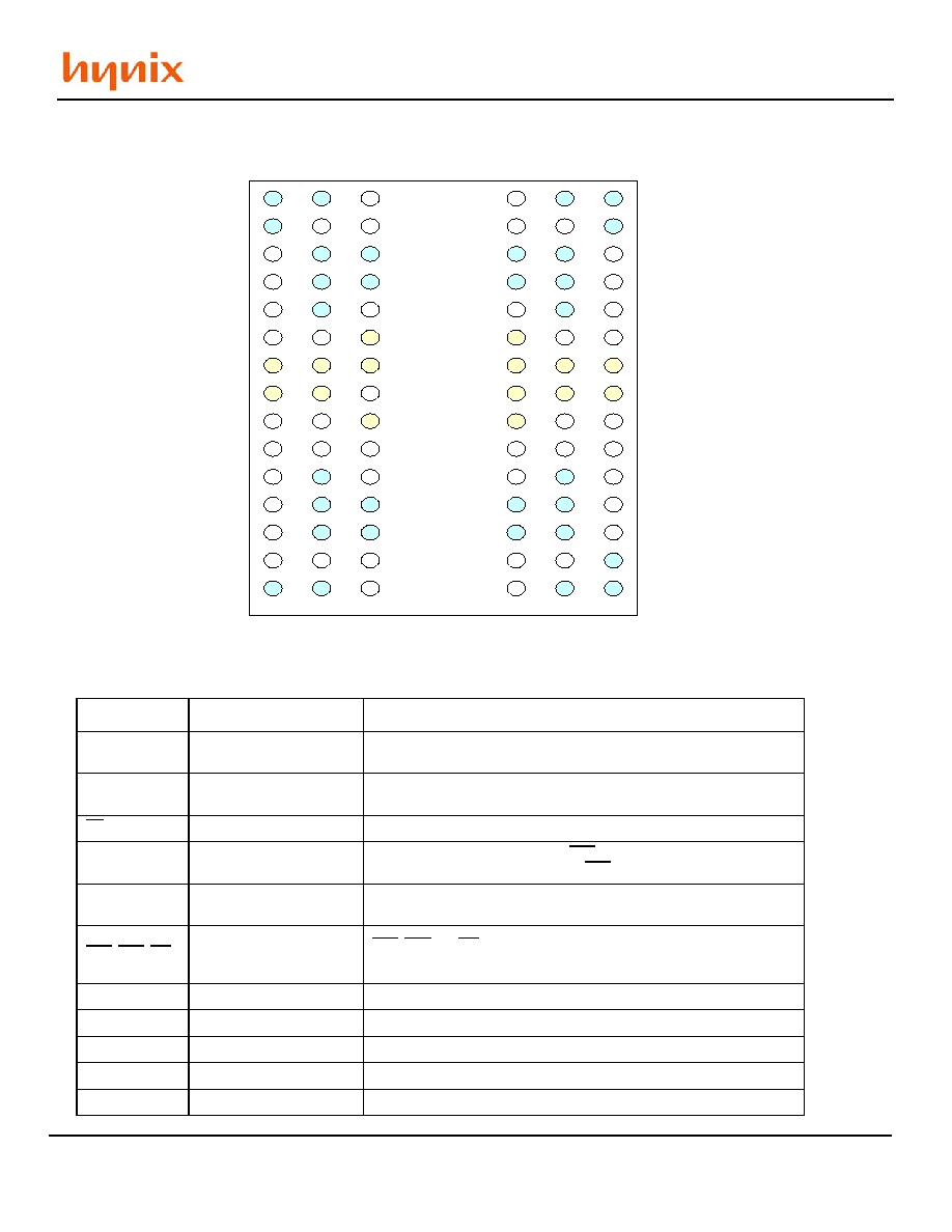
Ball CONFIGURATION ( HY5V22F-ISeries)
Ball DESCRIPTION
PIN
PIN NAME
DESCRIPTION
CLK
Clock
The system clock input. All other inputs are registered to the SDRAM on the
rising edge of CLK.
CKE
Clock Enable
Controls internal clock signal and when deactivated, the SDRAM will be one
of the states among power down, suspend or self refresh
CS
Chip Select
Enables or disables all inputs except CLK, CKE and DQM
BA0, BA1
Bank Address
Selects bank to be activated during RAS activity
Selects bank to be read/written during CAS activity
A0 ~ A11
Address
Row Address : RA0 ~ RA11, Column Address : CA0 ~ CA7
Auto-precharge flag : A10
RAS, CAS, WE
Row Address Strobe,
Column Address Strobe,
Write Enable
RAS, CAS and WE define the operation
Refer function truth table for details
DQM0~3
Data Input/Output Mask
Controls output buffers in read mode and masks input data in write mode
DQ0 ~ DQ31
Data Input/Output
Multiplexed data input / output pin
V
DD
/V
SS
Power Supply/Ground
Power supply for internal circuits and input buffers
V
DDQ
/V
SSQ
Data Output Power/Ground
Power supply for output buffers
NC
No Connection
No connection
T o p V ie w
A
B
C
D
E
F
G
H
J
K
L
M
N
P
R
D Q 2 6
D Q 2 4
V S S
D Q 2 8
V D D Q
V S S Q
V S S Q
D Q 2 7
D Q 2 5
V S S Q
D Q 2 9
D Q 3 0
V D D Q
D Q 3 1
N C
V S S
D Q M 3
A 3
A 4
A 5
A 6
A 7
A 8
N C
C L K
C K E
A 9
D Q M 1
N C
N C
V D D Q
D Q 8
V S S
V S S Q
D Q 1 0
D Q 9
V S S Q
D Q 1 2
D Q 1 4
D Q 1 1
V D D Q
V S S Q
D Q 1 3
D Q 1 5
V S S
V D D
D Q 2 3
D Q 2 1
V D D Q
V S S Q
D Q 1 9
D Q 2 2
D Q 2 0
V D D Q
D Q 1 7
D Q 1 8
V D D Q
N C
D Q 1 6
V S S Q
A 2
D Q M 2
V D D
A 1 0
A 0
A 1
N C
B A 1
A 1 1
B A 0
/C S
/R A S
/C A S
/W E
D Q M 0
V D D
D Q 7
V S S Q
D Q 6
D Q 5
V D D Q
D Q 1
D Q 3
V D D Q
V D D Q
V S S Q
D Q 4
V D D
D Q 0
D Q 2
1
2
3
7
8
9
4
5
6
A
B
C
D
E
F
G
H
J
K
L
M
N
P
R
D Q 2 6
D Q 2 4
V S S
D Q 2 8
V D D Q
V S S Q
V S S Q
D Q 2 7
D Q 2 5
V S S Q
D Q 2 9
D Q 3 0
V D D Q
D Q 3 1
N C
V S S
D Q M 3
A 3
A 4
A 5
A 6
A 7
A 8
N C
C L K
C K E
A 9
D Q M 1
N C
N C
V D D Q
D Q 8
V S S
V S S Q
D Q 1 0
D Q 9
V S S Q
D Q 1 2
D Q 1 4
D Q 1 1
V D D Q
V S S Q
D Q 1 3
D Q 1 5
V S S
V D D
D Q 2 3
D Q 2 1
V D D Q
V S S Q
D Q 1 9
D Q 2 2
D Q 2 0
V D D Q
D Q 1 7
D Q 1 8
V D D Q
N C
D Q 1 6
V S S Q
A 2
D Q M 2
V D D
A 1 0
A 0
A 1
N C
B A 1
A 1 1
B A 0
/C S
/R A S
/C A S
/W E
D Q M 0
V D D
D Q 7
V S S Q
D Q 6
D Q 5
V D D Q
D Q 1
D Q 3
V D D Q
V D D Q
V S S Q
D Q 4
V D D
D Q 0
D Q 2
1
2
3
7
8
9
4
5
6
Rev. 0.6/Nov. 02 4
HY57V283220T-I / HY5V22F-I
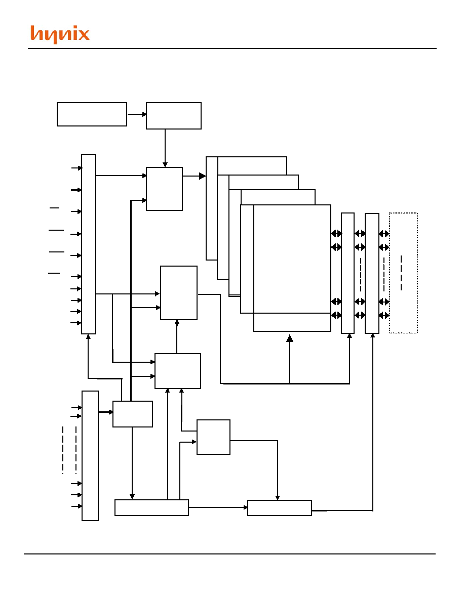
FUNCTIONAL BLOCK DIAGRAM
1Mbit x 4banks x 32 I/O Synchronous DRAM
X d
e
c
o
d
e
r
S
t
ate M
a
c
h
i
n
e
A0
A1
A11
BA0
BA1
A
d
d
r
es
s bu
ffe
r
s
Address
Register
Mode Register
Row
Pre
Decoder
Column
Pre
Decoder
Column Add
Counter
Row Active
Column
Active
Burst
Counter
Data Out Control
CAS Latency
Refresh
Counter
DQ0
DQ1
DQ30
DQ31
Self Refresh Logic
& Timer
Pipe Line Control
I/O B
u
ffer &
Logic
Bank Select
Se
nse AM
P
&
I/O
Ga
t
e
CLK
CKE
CS
RAS
CAS
WE
DQM0
DQM1
DQM2
DQM3
x32 Bank 3
X
de
co
de
r
X
de
co
de
r
Memory
Cell
Array
Y decoder
X
d
e
c
ode
r
1M x32 Bank 0
1M x32 Bank 1
1M x32 Bank 2
1M
X d
e
c
o
d
e
r
X d
e
c
o
d
e
r
S
t
ate M
a
c
h
i
n
e
A0
A1
A11
BA0
BA1
A
d
d
r
es
s bu
ffe
r
s
Address
Register
Mode Register
Row
Pre
Decoder
Column
Pre
Decoder
Column Add
Counter
Row Active
Column
Active
Burst
Counter
Data Out Control
CAS Latency
Refresh
Counter
DQ0
DQ1
DQ30
DQ31
Self Refresh Logic
& Timer
Pipe Line Control
I/O B
u
ffer &
Logic
Bank Select
Se
nse AM
P
&
I/O
Ga
t
e
CLK
CKE
CS
RAS
CAS
WE
DQM0
DQM1
DQM2
DQM3
x32 Bank 3
X
de
co
de
r
X
de
co
de
r
X
de
co
de
r
X
de
co
de
r
Memory
Cell
Array
Y decoder
X
d
e
c
ode
r
Memory
Cell
Array
Y decoder
X
d
e
c
ode
r
1M x32 Bank 0
1M x32 Bank 1
1M x32 Bank 2
1M
Rev. 0.6/Nov. 02 5
HY57V283220T-I / HY5V22F-I
ABSOLUTE MAXIMUM RATINGS
Note : Operation at above absolute maximum rating can adversely affect device reliability
DC OPERATING CONDITION
(TA=-40 to 85
°C)
Note :
1.All voltages are referenced to V
SS
= 0V
2.V
IH
(max) is acceptable 5.6V AC pulse width with
3ns of duration with no input clamp diodes
3.V
IL
(min) is acceptable -2.0V AC pulse width with
3ns of duration with no input clamp diodes
AC OPERATING CONDITION
(TA=-40 to 85
°C, 3.0V V
DD
3.6V, V
SS
=0V - Note1)
Note :
1.Output load to measure access times is equivalent to two TTL gates and one capacitor (30pF)
For details, refer to AC/DC output load circuit
Parameter
Symbol
Rating
Unit
Ambient Temperature
T
A
-40 ~ 85
°C
Storage Temperature
T
STG
-55 ~ 125
°C
Voltage on Any Pin relative to V
SS
V
IN
, V
OUT
-1.0 ~ 4.6
V
Voltage on V
DD
relative to V
SS
V
DD,
V
DDQ
-1.0 ~ 4.6
V
Short Circuit Output Current
I
OS
50
mA
Power Dissipation
P
D
1
W
Soldering Temperature
Time
T
SOLDER
260
10
°C Sec
Parameter
Symbol
Min
Typ.
Max
Unit
Note
Power Supply Voltage
V
DD
, V
DDQ
3.135
3.3
3.6
V
1
Input high voltage
V
IH
2.0
3.0
V
DDQ
+ 0.3
V
1,2
Input low voltage
V
IL
V
SSQ
- 0.3
0
0.8
V
1,3
Parameter
Symbol
Value
Unit
Note
AC input high / low level voltage
V
IH
/ V
IL
2.4/0.4
V
Input timing measurement reference level voltage
Vtrip
1.4
V
Input rise / fall time
tR / tF
1
ns
Output timing measurement reference level
Voutref
1.4
V
Output load capacitance for access time measurement
CL
30
pF
1