
HY5DU56422A(L)F
HY5DU56822A(L)F
HY5DU561622A(L)F
256M-S DDR SDRAM
HY5DU56422A(L)F
HY5DU56822A(L)F
HY5DU561622A(L)F
This document is a general product description and is subject to change without notice. Hynix semiconductor does not assume any
responsibility for use of circuits described. No patent licenses are implied.
Rev. 0.1/ Apr. 02 1

Rev. 0.1/Apr. 02 2
HY5DU56422A(L)F
HY5DU56822A(L)F
HY5DU561622A(L)F
Revision History
1. Revision 0.1 (Apr. 02)
1) Define Preliminary Specification
DESCRIPTION
The Hynix HY5DU56422, HY5DU56822 and HY5DU561622 are a 268,435,456-bit CMOS Double Data Rate(DDR) Syn-
chronous DRAM, ideally suited for the main memory applications which requires large memory density and high band-
width.
The Hynix 256Mb DDR SDRAMs offer fully synchronous operations referenced to both rising and falling edges of the
clock. While all addresses and control inputs are latched on the rising edges of the CK (falling edges of the /CK), Data,
Data strobes and Write data masks inputs are sampled on both rising and falling edges of it. The data paths are inter-
nally pipelined and 2-bit prefetched to achieve very high bandwidth. All input and output voltage levels are compatible
with SSTL_2.
FEATURES
PRELIMINARY
Rev. 0.1 / Apr. 02 3
HY5DU56422A(L)F
HY5DU56822A(L)F
HY5DU561622A(L)F
�
V
DD
, V
DDQ
= 2.5V +/- 0.2V
�
All inputs and outputs are compatible with SSTL_2
interface
�
Fully differential clock inputs (CK, /CK) operation
�
Double data rate interface
�
Source synchronous - data transaction aligned to
bidirectional data strobe (DQS)
�
x16 device has two bytewide data strobes (UDQS,
LDQS) per each x8 I/O
�
Data outputs on DQS edges when read (edged DQ)
Data inputs on DQS centers when write (centered
DQ)
�
On chip DLL align DQ and DQS transition with CK
transition
�
DM mask write data-in at the both rising and falling
edges of the data strobe
�
All addresses and control inputs except data, data
strobes and data masks latched on the rising edges
of the clock
�
Programmable CAS latency 1.5, 2, 2.5 and 3
supported
�
Programmable burst length 2 / 4 / 8 with both
sequential and interleave mode
�
Internal four bank operations with single pulsed
/RAS
�
tRAS Lock-out function supported
�
Auto refresh and Self refresh supported
�
8192 refresh cycles / 64ms
�
60 Ball FBGA Package Type
�
Full and Half strength driver option controlled by
EMRS
ORDERING INFORMATION
* X means speed grade
Part No.
Configuration
Package
HY5DU56422A(L)F-X*
64Mx4
60 Ball
FBGA
HY5DU56822A(L)F-X*
32Mx8
HY5DU561622A(L)F-X*
16Mx16
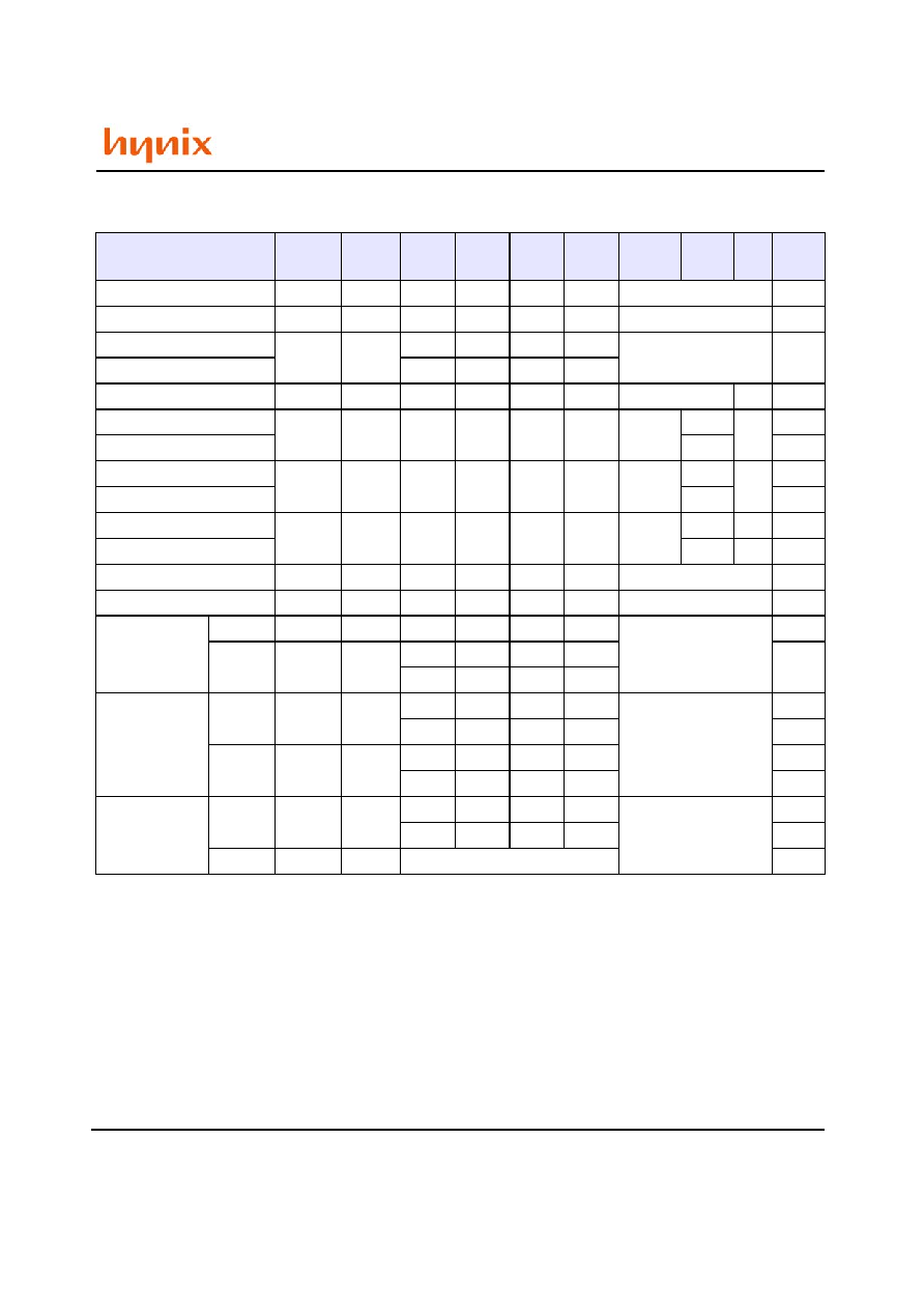
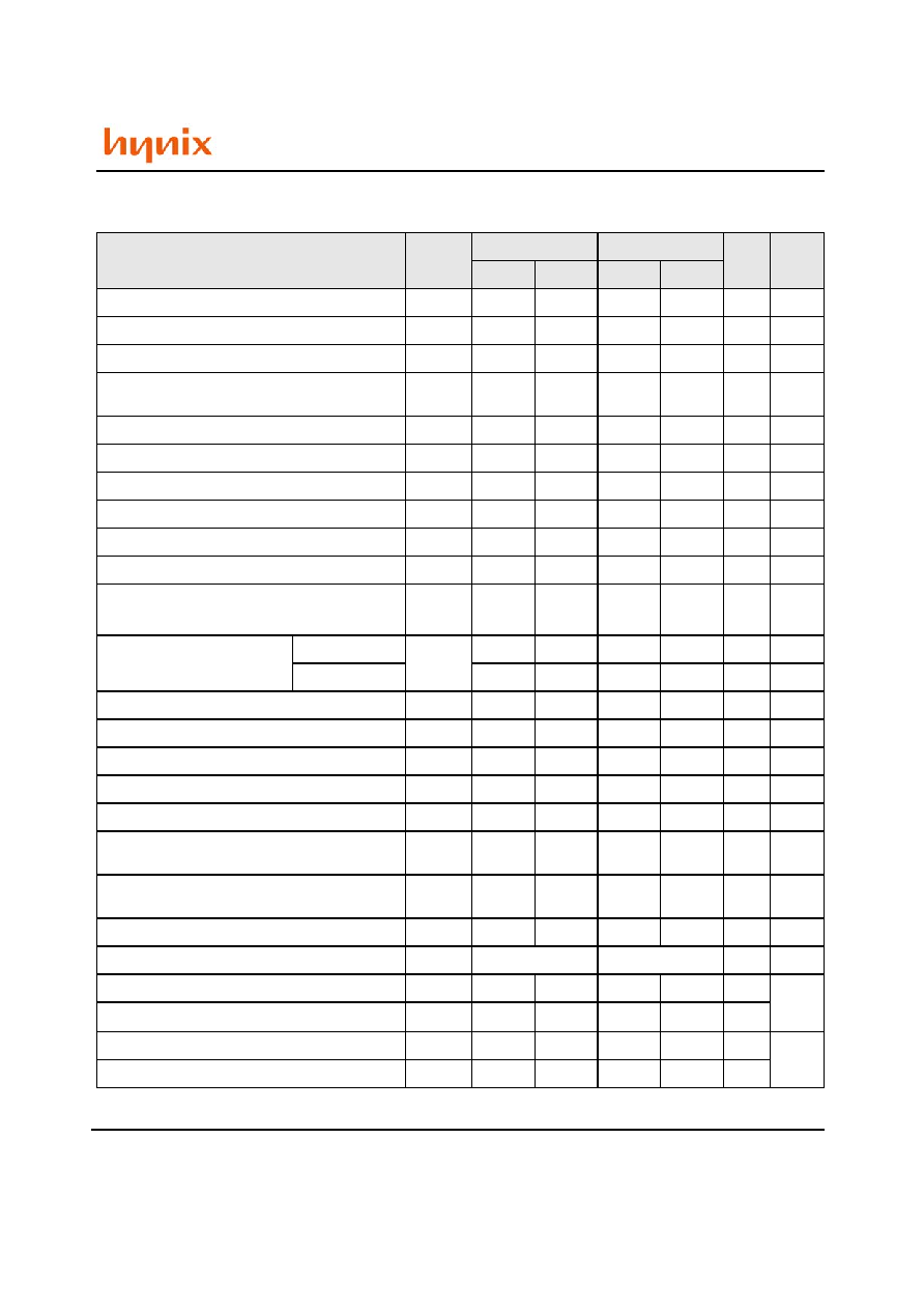
OPERATING FREQUENCY
Grade
CL2
CL2.5
Remark
(CL-tRCD-tRP)
- J
133MHz
166MHz
DDR333 (2.5-3-3)
- M
133MHz
133MHz
DDR266 (2-2-2)
- K
133MHz
133MHz
DDR266A (2-3-3)
- H
100MHz
133MHz
DDR266B (2.5-3-3)
- L
100MHz
125MHz
DDR200 (2-2-2)
* CL1.5 @ DDR200 supported
* CL3 supported
Rev. 0.1/Apr. 02 4
HY5DU56422A(L)F
HY5DU56822A(L)F
HY5DU561622A(L)F
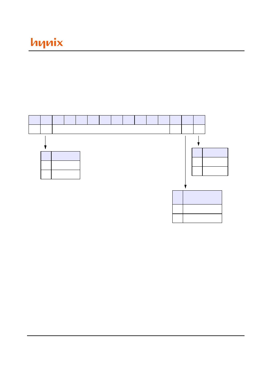
PIN CONFIGURATION
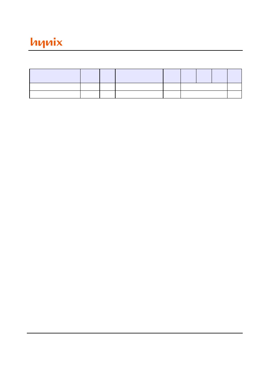
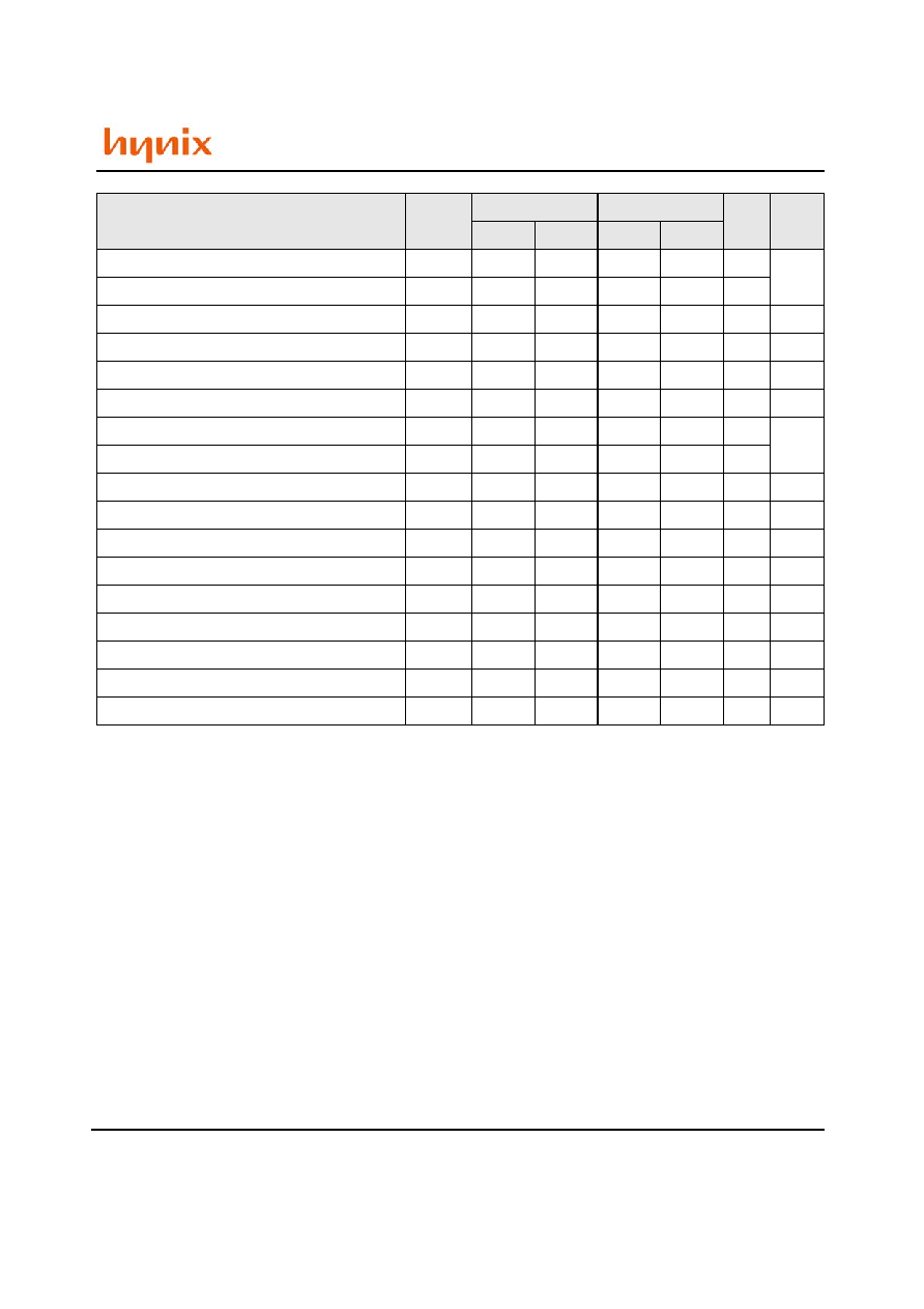
ROW AND COLUMN ADDRESS TABLE
ITEMS
64Mx4
32Mx8
16Mx16
Organization
16M x 4 x 4banks
8M x 8 x 4banks
4M x 16 x 4banks
Row Address
A0 - A12
A0 - A12
A0 - A12
Column Address
A0-A9, A11
A0-A9
A0-A8
Bank Address
BA0, BA1
BA0, BA1
BA0, BA1
Auto Precharge Flag
A10
A10
A10
Refresh
8K
8K
8K
Rev. 0.1/Apr. 02 5
HY5DU56422A(L)F
HY5DU56822A(L)F
HY5DU561622A(L)F
PIN DESCRIPTION
PIN
TYPE
DESCRIPTION
CK, /CK
Input
Clock: CK and /CK are differential clock inputs. All address and control input signals are
sampled on the crossing of the positive edge of CK and negative edge of /CK. Output
(read) data is referenced to the crossings of CK and /CK (both directions of crossing).
CKE
Input
Clock Enable: CKE HIGH activates, and CKE LOW deactivates internal clock signals, and
device input buffers and output drivers. Taking CKE LOW provides PRECHARGE POWER
DOWN and SELF REFRESH operation (all banks idle), or ACTIVE POWER DOWN (row
ACTIVE in any bank). CKE is synchronous for POWER DOWN entry and exit, and for SELF
REFRESH entry. CKE is asynchronous for SELF REFRESH exit, and for output disable. CKE
must be maintained high throughout READ and WRITE accesses. Input buffers, excluding
CK, /CK and CKE are disabled during POWER DOWN. Input buffers, excluding CKE are
disabled during SELF REFRESH. CKE is an SSTL_2 input, but will detect an LVCMOS LOW
level after Vdd is applied.
/CS
Input
Chip Select : Enables or disables all inputs except CK, /CK, CKE, DQS and DM. All com-
mands are masked when CS is registered high. CS provides for external bank selection on
systems with multiple banks. CS is considered part of the command code.
BA0, BA1
Input
Bank Address Inputs: BA0 and BA1 define to which bank an ACTIVE, Read, Write or PRE-
CHARGE command is being applied.
A0 ~ A12
Input
Address Inputs: Provide the row address for ACTIVE commands, and the column address
and AUTO PRECHARGE bit for READ/WRITE commands, to select one location out of the
memory array in the respective bank. A10 is sampled during a precharge command to
determine whether the PRECHARGE applies to one bank (A10 LOW) or all banks (A10
HIGH). If only one bank is to be precharged, the bank is selected by BA0, BA1. The
address inputs also provide the op code during a MODE REGISTER SET command. BA0
and BA1 define which mode register is loaded during the MODE REGISTER SET command
(MRS or EMRS).
/RAS, /CAS, /WE
Input
Command Inputs: /RAS, /CAS and /WE (along with /CS) define the command being
entered.
DM
(LDM, UDM)
Input
Input Data Mask: DM is an input mask signal for write data. Input data is masked when
DM is sampled HIGH along with that input data during a WRITE access. DM is sampled
on both edges of DQS. Although DM pins are input only, the DM loading matches the DQ
and DQS loading. For the x16, LDM corresponds to the data on DQ0-Q7; UDM corre-
sponds to the data on DQ8-Q15.
DQS
(LDQS, UDQS)
I/O
Data Strobe: Output with read data, input with write data. Edge aligned with read data,
centered in write data. Used to capture write data. For the x16, LDQS corresponds to the
data on DQ0-Q7; UDQS corresponds to the data on DQ8-Q15.
DQ
I/O
Data input / output pin : Data bus
V
DD
/V
SS
Supply
Power supply for internal circuits and input buffers.
V
DDQ
/V
SSQ
Supply
Power supply for output buffers for noise immunity.
V
REF
Supply
Reference voltage for inputs for SSTL interface.
NC
NC
No connection.

Rev. 0.1/Apr. 02 6
HY5DU56422A(L)F
HY5DU56822A(L)F
HY5DU561622A(L)F
Command
Decoder
CLK
/CLK
CKE
/CS
/RAS
/CAS
/WE
Address
Buffer
ADD
Bank
Control
16Mx4 / Bank0
Column Decoder
Column Address
Counter
S
e
nse A
M
P
2
-
bi
t
P
r
e
f
et
c
h
U
n
i
t
16Mx4 / Bank1
16Mx4 / Bank2
16Mx4 / Bank3
Mode
Register
Row
Decoder
In
p
u
t B
u
f
f
e
r
O
u
t
put
B
u
f
f
er
Data Strobe
Transmitter
Data Strobe
Receiver
DQS
DQS
Write Data Register
2-bit Prefetch Unit
DQS
DQ[0:3]
8
4
4
8
BA
DLL
Block
CLK_DLL
CLK,
/CLK
Mode
Register
DM
FUNCTIONAL BLOCK DIAGRAM (64Mx4)
4Banks x 16Mbit x 4 I/O Double Data Rate Synchronous DRAM
Rev. 0.1/Apr. 02 7
HY5DU56422A(L)F
HY5DU56822A(L)F
HY5DU561622A(L)F
Command
Decoder
CLK
/CLK
CKE
/CS
/RAS
/CAS
/WE
Address
Buffer
ADD
Bank
Control
8Mx8 / Bank0
Column Decoder
Column Address
Counter
Se
n
s
e
AM
P
2-
bi
t
P
r
e
f
et
c
h
U
n
i
t
8Mx8 / Bank1
8Mx8 / Bank2
8Mx8 / Bank3
Mode
Register
Row
Decoder
In
p
u
t B
u
ffe
r
O
u
t
p
ut
B
u
f
f
er
Data Strobe
Transmitter
Data Strobe
Receiver
DQS
DQS
Write Data Register
2-bit Prefetch Unit
DQS
DQ[0:7]
16
8
8
16
BA
DLL
Block
CLK_DLL
CLK,
/CLK
Mode
Register
DM
FUNCTIONAL BLOCK DIAGRAM (32Mx8)
4Banks x 8Mbit x 8 I/O Double Data Rate Synchronous DRAM

Rev. 0.1/Apr. 02 8
HY5DU56422A(L)F
HY5DU56822A(L)F
HY5DU561622A(L)F
Command
Decoder
CLK
/CLK
CKE
/CS
/RAS
/CAS
/WE
Address
Buffer
ADD
Bank
Control
4Mx16 / Bank0
Column Decoder
Column Address
Counter
S
e
nse A
M
P
2
-
bi
t
P
r
e
f
et
c
h
U
n
i
t
4Mx16 / Bank1
4Mx16 / Bank2
4Mx16 / Bank3
Mode
Register
Row
Decoder
In
p
u
t B
u
f
f
e
r
O
u
t
put
B
u
f
f
er
Data Strobe
Transmitter
Data Strobe
Receiver
LDQS, UDQS
LDQS
UDQS
Write Data Register
2-bit Prefetch Unit
LDQS, UDQS
DQ[0:15]
32
16
16
32
BA
DLL
Block
CLK_DLL
CLK,
/CLK
Mode
Register
LDM, UDM
FUNCTIONAL BLOCK DIAGRAM (16Mx16)
4Banks x 4Mbit x 16 I/O Double Data Rate Synchronous DRAM
Rev. 0.1/Apr. 02 9
HY5DU56422A(L)F
HY5DU56822A(L)F
HY5DU561622A(L)F
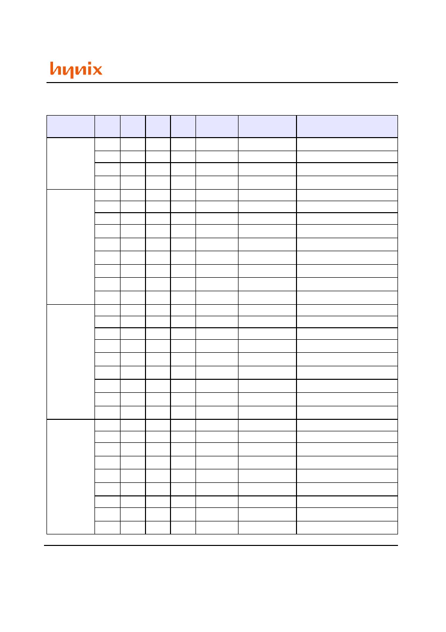
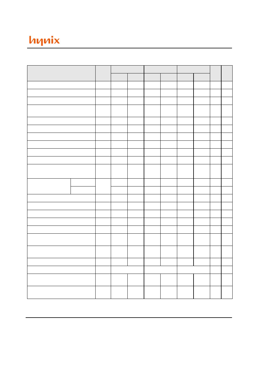
SIMPLIFIED COMMAND TRUTH TABLE
Command
CKEn-1
CKEn
CS
RAS
CAS
WE
ADDR
A10/
AP
BA
Note
Extended Mode Register Set
H
X
L
L
L
L
OP code
1,2
Mode Register Set
H
X
L
L
L
L
OP code
1,2
Device Deselect
H
X
H
X
X
X
X
1
No Operation
L
H
H
H
Bank Active
H
X
L
L
H
H
RA
V
1
Read
H
X
L
H
L
H
CA
L
V
1
Read with Autoprecharge
H
1,3
Write
H
X
L
H
L
L
CA
L
V
1
Write with Autoprecharge
H
1,4
Precharge All Banks
H
X
L
L
H
L
X
H
X
1,5
Precharge selected Bank
L
V
1
Read Burst Stop
H
X
L
H
H
L
X
1
Auto Refresh
H
H
L
L
L
H
X
1
Self Refresh
Entry
H
L
L
L
L
H
X
1
Exit
L
H
H
X
X
X
1
L
H
H
H
Precharge Power
Down Mode
Entry
H
L
H
X
X
X
X
1
L
H
H
H
1
Exit
L
H
H
X
X
X
1
L
H
H
H
1
Active Power
Down Mode
Entry
H
L
H
X
X
X
X
1
L
V
V
V
1
Exit
L
H
X
1
Note :
1. LDM/UDM states are Don't Care. Refer to below Write Mask Truth Table.
2. OP Code(Operand Code) consists of A0~A11 and BA0~BA1 used for Mode Register setting duing Extended MRS or MRS.
Before entering Mode Register Set mode, all banks must be in a precharge state and MRS command can be issued after tRP
period from Prechagre command.
3. If a Read with Autoprecharge command is detected by memory component in CK(n), then there will be no command presented
to activated bank until CK(n+BL/2+tRP).
4. If a Write with Autoprecharge command is detected by memory component in CK(n), then there will be no command presented
to activated bank until CK(n+BL/2+1+tDPL+tRP). Last Data-In to Prechage delay(tDPL) which is also called Write Recovery Time
(tWR) is needed to guarantee that the last data has been completely written.
5. If A10/AP is High when Precharge command being issued, BA0/BA1 are ignored and all banks are selected to be
precharged.
( H=Logic High Level, L=Logic Low Level, X=Don't Care, V=Valid Data Input, OP Code=Operand Code, NOP=No Operation )
Rev. 0.1/Apr. 02 10
HY5DU56422A(L)F
HY5DU56822A(L)F
HY5DU561622A(L)F
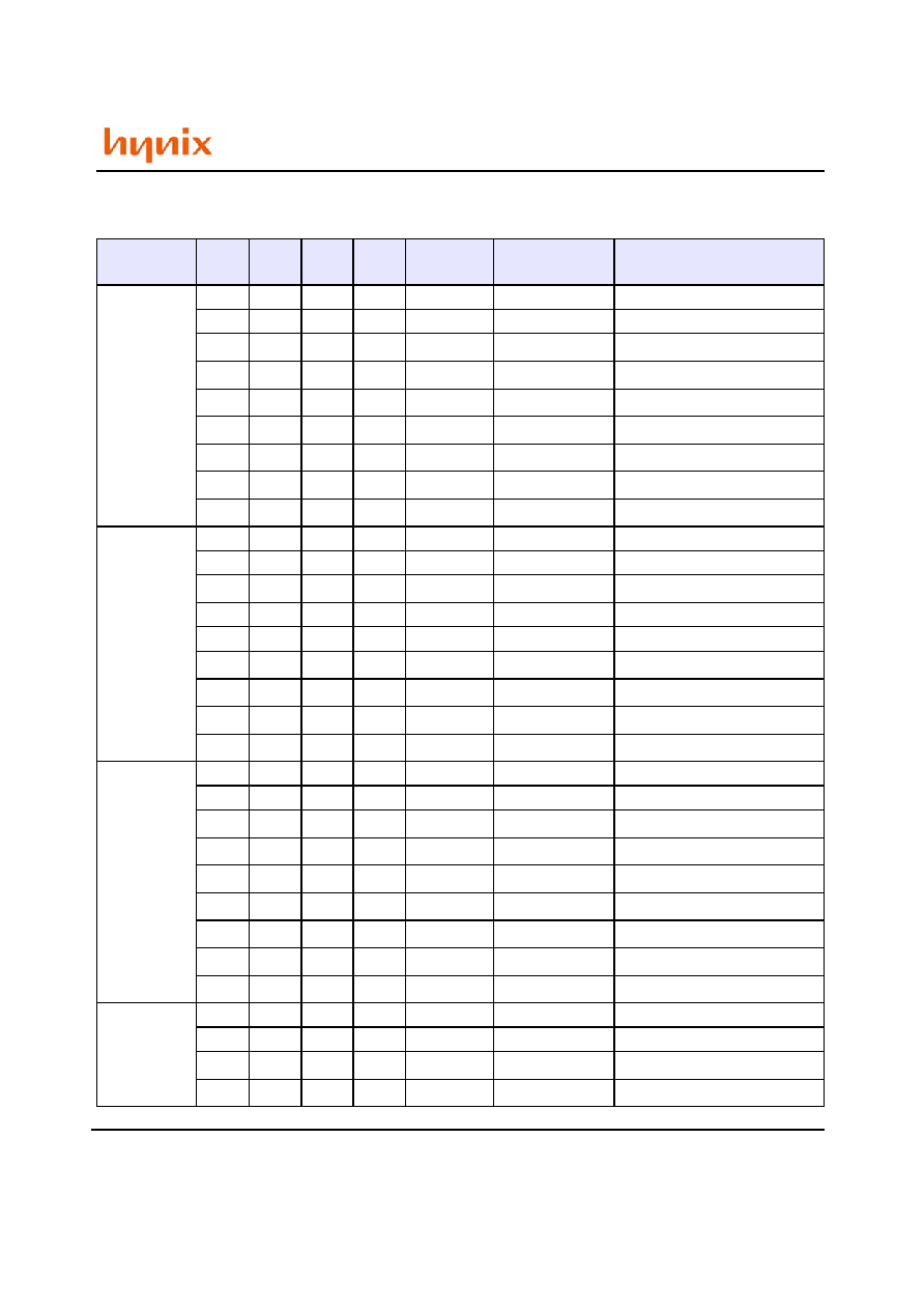
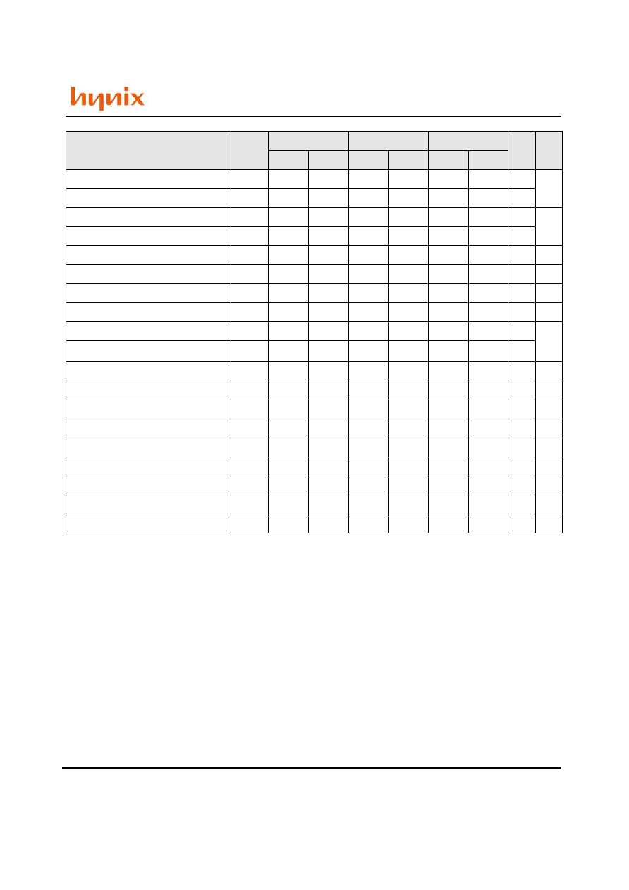
WRITE MASK TRUTH TABLE
Function
CKEn-1
CKEn
/CS, /RAS, /CAS, /WE
DM
ADD
R
A10/
AP
BA
Note
Data Write
H
X
X
L
X
1
Data-In Mask
H
X
X
H
X
1
Note :
1.
Write Mask command masks burst write data with reference to LDQS/UDQS(Data Strobes) and it is not related
with read data. In case of x16 data I/O, LDM and UDM control lower byte(DQ0~7) and Upper byte(DQ8~15)
respectively.

Rev. 0.1/Apr. 02 11
HY5DU56422A(L)F
HY5DU56822A(L)F
HY5DU561622A(L)F
OPERATION COMMAND TRUTH TABLE-I
Current
State
/CS
/RAS
/CAS
/WE
Address
Command
Action
IDLE
H
X
X
X
X
DSEL
NOP or power down
3
L
H
H
H
X
NOP
NOP or power down
3
L
H
H
L
X
BST
ILLEGAL
4
L
H
L
H
BA, CA, AP
READ/READAP
ILLEGAL
4
L
H
L
L
BA, CA, AP
WRITE/WRITEAP
ILLEGAL
4
L
L
H
H
BA, RA
ACT
Row Activation
L
L
H
L
BA, AP
PRE/PALL
NOP
L
L
L
H
X
AREF/SREF
Auto Refresh or Self Refresh
5
L
L
L
L
OPCODE
MRS
Mode Register Set
ROW
ACTIVE
H
X
X
X
X
DSEL
NOP
L
H
H
H
X
NOP
NOP
L
H
H
L
X
BST
ILLEGAL
4
L
H
L
H
BA, CA, AP
READ/READAP
Begin read : optional AP
6
L
H
L
L
BA, CA, AP
WRITE/WRITEAP
Begin write : optional AP
6
L
L
H
H
BA, RA
ACT
ILLEGAL
4
L
L
H
L
BA, AP
PRE/PALL
Precharge
7
L
L
L
H
X
AREF/SREF
ILLEGAL
11
L
L
L
L
OPCODE
MRS
ILLEGAL
11
READ
H
X
X
X
X
DSEL
Continue burst to end
L
H
H
H
X
NOP
Continue burst to end
L
H
H
L
X
BST
Terminate burst
L
H
L
H
BA, CA, AP
READ/READAP
Term burst, new read:optional AP
8
L
H
L
L
BA, CA, AP
WRITE/WRITEAP
ILLEGAL
L
L
H
H
BA, RA
ACT
ILLEGAL
4
L
L
H
L
BA, AP
PRE/PALL
Term burst, precharge
L
L
L
H
X
AREF/SREF
ILLEGAL
11
L
L
L
L
OPCODE
MRS
ILLEGAL
11
WRITE
H
X
X
X
X
DSEL
Continue burst to end
L
H
H
H
X
NOP
Continue burst to end
L
H
H
L
X
BST
ILLEGAL
4
L
H
L
H
BA, CA, AP
READ/READAP
Term burst, new read:optional AP
8
L
H
L
L
BA, CA, AP
WRITE/WRITEAP
Term burst, new write:optional AP
Rev. 0.1/Apr. 02 12
HY5DU56422A(L)F
HY5DU56822A(L)F
HY5DU561622A(L)F
OPERATION COMMAND TRUTH TABLE-II
Current
State
/CS
/RAS
/CAS
/WE
Address
Command
Action
WRITE
L
L
H
H
BA, RA
ACT
ILLEGAL
4
L
L
H
L
BA, AP
PRE/PALL
Term burst, precharge
L
L
L
H
X
AREF/SREF
ILLEGAL
11
L
L
L
L
OPCODE
MRS
ILLEGAL
11
READ
WITH
AUTOPRE-
CHARGE
H
X
X
X
X
DSEL
Continue burst to end
L
H
H
H
X
NOP
Continue burst to end
L
H
H
L
X
BST
ILLEGAL
L
H
L
H
BA, CA, AP
READ/READAP
ILLEGAL
10
L
H
L
L
BA, CA, AP
WRITE/WRITEAP
ILLEGAL
10
L
L
H
H
BA, RA
ACT
ILLEGAL
4,10
L
L
H
L
BA, AP
PRE/PALL
ILLEGAL
4,10
L
L
L
H
X
AREF/SREF
ILLEGAL
11
L
L
L
L
OPCODE
MRS
ILLEGAL
11
WRITE
AUTOPRE-
CHARGE
H
X
X
X
X
DSEL
Continue burst to end
L
H
H
H
X
NOP
Continue burst to end
L
H
H
L
X
BST
ILLEGAL
L
H
L
H
BA, CA, AP
READ/READAP
ILLEGAL
10
L
H
L
L
BA, CA, AP
WRITE/WRITEAP
ILLEGAL
10
L
L
H
H
BA, RA
ACT
ILLEGAL
4,10
L
L
H
L
BA, AP
PRE/PALL
ILLEGAL
4,10
L
L
L
H
X
AREF/SREF
ILLEGAL
11
L
L
L
L
OPCODE
MRS
ILLEGAL
11
PRE-
CHARGE
H
X
X
X
X
DSEL
NOP-Enter IDLE after tRP
L
H
H
H
X
NOP
NOP-Enter IDLE after tRP
L
H
H
L
X
BST
ILLEGAL
4
L
H
L
H
BA, CA, AP
READ/READAP
ILLEGAL
4,10
L
H
L
L
BA, CA, AP
WRITE/WRITEAP
ILLEGAL
4,10
L
L
H
H
BA, RA
ACT
ILLEGAL
4,10
L
L
H
L
BA, AP
PRE/PALL
NOP-Enter IDLE after tRP
L
L
L
H
X
AREF/SREF
ILLEGAL
11
L
L
L
L
OPCODE
MRS
ILLEGAL
11
Rev. 0.1/Apr. 02 13
HY5DU56422A(L)F
HY5DU56822A(L)F
HY5DU561622A(L)F
OPERATION COMMAND TRUTH TABLE-III
Current
State
/CS
/RAS
/CAS
/WE
Address
Command
Action
ROW
ACTIVATING
H
X
X
X
X
DSEL
NOP - Enter ROW ACT after tRCD
L
H
H
H
X
NOP
NOP - Enter ROW ACT after tRCD
L
H
H
L
X
BST
ILLEGAL
4
L
H
L
H
BA, CA, AP
READ/READAP
ILLEGAL
4,10
L
H
L
L
BA, CA, AP
WRITE/WRITEAP
ILLEGAL
4,10
L
L
H
H
BA, RA
ACT
ILLEGAL
4,9,10
L
L
H
L
BA, AP
PRE/PALL
ILLEGAL
4,10
L
L
L
H
X
AREF/SREF
ILLEGAL
11
L
L
L
L
OPCODE
MRS
ILLEGAL
11
WRITE
RECOVERING
H
X
X
X
X
DSEL
NOP - Enter ROW ACT after tWR
L
H
H
H
X
NOP
NOP - Enter ROW ACT after tWR
L
H
H
L
X
BST
ILLEGAL
4
L
H
L
H
BA, CA, AP
READ/READAP
ILLEGAL
L
H
L
L
BA, CA, AP
WRITE/WRITEAP
ILLEGAL
L
L
H
H
BA, RA
ACT
ILLEGAL
4,10
L
L
H
L
BA, AP
PRE/PALL
ILLEGAL
4,11
L
L
L
H
X
AREF/SREF
ILLEGAL
11
L
L
L
L
OPCODE
MRS
ILLEGAL
11
WRITE
RECOVERING
WITH
AUTOPRE-
CHARGE
H
X
X
X
X
DSEL
NOP - Enter precharge after tDPL
L
H
H
H
X
NOP
NOP - Enter precharge after tDPL
L
H
H
L
X
BST
ILLEGAL
4
L
H
L
H
BA, CA, AP
READ/READAP
ILLEGAL
4,8,10
L
H
L
L
BA, CA, AP
WRITE/WRITEAP
ILLEGAL
4,10
L
L
H
H
BA, RA
ACT
ILLEGAL
4,10
L
L
H
L
BA, AP
PRE/PALL
ILLEGAL
4,11
L
L
L
H
X
AREF/SREF
ILLEGAL
11
L
L
L
L
OPCODE
MRS
ILLEGAL
11
REFRESHING
H
X
X
X
X
DSEL
NOP - Enter IDLE after tRC
L
H
H
H
X
NOP
NOP - Enter IDLE after tRC
L
H
H
L
X
BST
ILLEGAL
11
L
H
L
H
BA, CA, AP
READ/READAP
ILLEGAL
11

Rev. 0.1/Apr. 02 14
HY5DU56422A(L)F
HY5DU56822A(L)F
HY5DU561622A(L)F
OPERATION COMMAND TRUTH TABLE-IV
Note :
1. H - Logic High Level, L - Logic Low Level, X - Don't Care, V - Valid Data Input,
BA - Bank Address, AP - AutoPrecharge Address, CA - Column Address, RA - Row Address, NOP - NO Operation.
2. All entries assume that CKE was active(high level) during the preceding clock cycle.
3. If both banks are idle and CKE is inactive(low level), then in power down mode.
4. Illegal to bank in specified state. Function may be legal in the bank indicated by Bank Address(BA) depending on the state of
that bank.
5. If both banks are idle and CKE is inactive(low level), then self refresh mode.
6. Illegal if tRCD is not met.
7. Illegal if tRAS is not met.
8. Must satisfy bus contention, bus turn around, and/or write recovery requirements.
9. Illegal if tRRD is not met.
10. Illegal for single bank, but legal for other banks in multi-bank devices.
11. Illegal for all banks.
Current
State
/CS
/RAS
/CAS
/WE
Address
Command
Action
WRITE
L
H
L
L
BA, CA, AP
WRITE/WRITEAP
ILLEGAL
11
L
L
H
H
BA, RA
ACT
ILLEGAL
11
L
L
H
L
BA, AP
PRE/PALL
ILLEGAL
11
L
L
L
H
X
AREF/SREF
ILLEGAL
11
L
L
L
L
OPCODE
MRS
ILLEGAL
11
MODE
REGISTER
ACCESSING
H
X
X
X
X
DSEL
NOP - Enter IDLE after tMRD
L
H
H
H
X
NOP
NOP - Enter IDLE after tMRD
L
H
H
L
X
BST
ILLEGAL
11
L
H
L
H
BA, CA, AP
READ/READAP
ILLEGAL
11
L
H
L
L
BA, CA, AP
WRITE/WRITEAP
ILLEGAL
11
L
L
H
H
BA, RA
ACT
ILLEGAL
11
L
L
H
L
BA, AP
PRE/PALL
ILLEGAL
11
L
L
L
H
X
AREF/SREF
ILLEGAL
11
L
L
L
L
OPCODE
MRS
ILLEGAL
11
Rev. 0.1/Apr. 02 15
HY5DU56422A(L)F
HY5DU56822A(L)F
HY5DU561622A(L)F
CKE FUNCTION TRUTH TABLE
Note :
When CKE=L, all DQ and DQS must be in Hi-Z state.
1. CKE and /CS must be kept high for a minimum of 200 stable input clocks before issuing any command.
2. All command can be stored after 2 clocks from low to high transition of CKE.
3. Illegal if CLK is suspended or stopped during the power down mode.
4. Self refresh can be entered only from the all banks idle state.
5. Disabling CLK may cause malfunction of any bank which is in active state.
Current
State
CKEn-
1
CKEn
/CS
/RAS
/CAS
/WE
/ADD
Action
SELF
REFRESH
1
H
X
X
X
X
X
X
INVALID
L
H
H
X
X
X
X
Exit self refresh, enter idle after tSREX
L
H
L
H
H
H
X
Exit self refresh, enter idle after tSREX
L
H
L
H
H
L
X
ILLEGAL
L
H
L
H
L
X
X
ILLEGAL
L
H
L
L
X
X
X
ILLEGAL
L
L
X
X
X
X
X
NOP, continue self refresh
POWER
DOWN
2
H
X
X
X
X
X
X
INVALID
L
H
H
X
X
X
X
Exit power down, enter idle
L
H
L
H
H
H
X
Exit power down, enter idle
L
H
L
H
H
L
X
ILLEGAL
L
H
L
H
L
X
X
ILLEGAL
L
H
L
L
X
X
X
ILLEGAL
L
L
X
X
X
X
X
NOP, continue power down mode
ALL BANKS
IDLE
4
H
H
X
X
X
X
X
See operation command truth table
H
L
L
L
L
H
X
Enter self refresh
H
L
H
X
X
X
X
Exit power down
H
L
L
H
H
H
X
Exit power down
H
L
L
H
H
L
X
ILLEGAL
H
L
L
H
L
X
X
ILLEGAL
H
L
L
L
H
X
X
ILLEGAL
H
L
L
L
L
L
X
ILLEGAL
L
L
X
X
X
X
X
NOP
ANY STATE
OTHER
THAN
ABOVE
H
H
X
X
X
X
X
See operation command truth table
H
L
X
X
X
X
X
ILLEGAL
5
L
H
X
X
X
X
X
INVALID
L
L
X
X
X
X
X
INVALID
Rev. 0.1/Apr. 02 16
HY5DU56422A(L)F
HY5DU56822A(L)F
HY5DU561622A(L)F
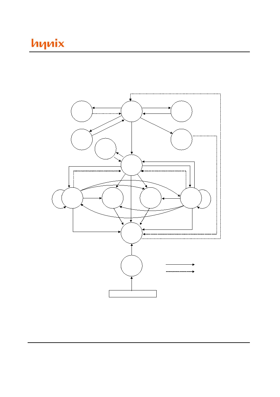
SIMPLIFIED STATE DIAGRAM
MRS
SREF
SREX
PDEN
PDEX
ACT
AREF
PDEX
PDEN
BST
READ
WRITE
WRITE
WRITEAP
WRITEAP
READ
READAP
READAP
PRE(PALL)
PRE(PALL)
PRE
(
PA
LL)
Command Input
Automatic Sequence
IDLE
AUTO
REFRESH
PRE-
CHARGE
POWER-UP
POWER APPLIED
MODE
REGISTER
SET
POWER
DOWN
WRITE
WITH
AUTOPRE-
CHARGE
POWER
DOWN
WRITE
READ
WITH
AUTOPRE-
CHARGE
BANK
ACTIVE
READ
SELF
REFRESH
Rev. 0.1/Apr. 02 17
HY5DU56422A(L)F
HY5DU56822A(L)F
HY5DU561622A(L)F
POWER-UP SEQUENCE AND DEVICE INITIALIZATION
DDR SDRAMs must be powered up and initialized in a predefined manner. Operational procedures other than those
specified may result in undefined operation. Except for CKE, inputs are not recognized as valid until after VREF is
applied. CKE is an SSTL_2 input, but will detect an LVCMOS LOW level after VDD is applied. Maintaining an LVCMOS
LOW level on CKE during power-up is required to guarantee that the DQ and DQS outputs will be in the High-Z state,
where they will remain until driven in normal operation (by a read access). After all power supply and reference volt-
ages are stable, and the clock is stable, the DDR SDRAM requires a 200us delay prior to applying an executable com-
mand.
Once the 200us delay has been satisfied, a DESELECT or NOP command should be applied, and CKE should be
brought HIGH. Following the NOP command, a PRECHARGE ALL command should be applied. Next a EXTENDED
MODE REGISTER SET command should be issued for the Extended Mode Register, to enable the DLL, then a MODE
REGISTER SET command should be issued for the Mode Register, to reset the DLL, and to program the operating
parameters. 200 clock cycles are required between the DLL reset and any command. During the 200 cycles of CK, for
DLL locking, executable commands are disallowed (a DESELECT or NOP command must be applied). After the 200
clock cycles, a PRECHARGE ALL command should be applied, placing the device in the all banks idle state.
Once in the idle state, two AUTO REFRESH cycles must be performed. Additionally, a MODE REGISTER SET command
for the Mode Register, with the reset DLL bit deactivated (i.e. to program operating parameters without resetting the
DLL) must be performed. Following these cycles, the DDR SDRAM is ready for normal operation.
1. Apply power - VDD, VDDQ, VTT, VREF in the following power up sequencing and attempt to maintain CKE at LVC-
MOS low state. (All the other input pins may be undefined.
No power sequencing is specified during power up or power down given the following cirteria :
� VDD and VDDQ are driven from a single power converter output.
� VTT is limited to 1.44V (reflecting VDDQ(max)/2 + 50mV VREF variation + 40mV VTT variation).
� VREF tracks VDDQ/2.
� A minimum resistance of 42 ohms (22 ohm series resistor + 22 ohm parallel resistor - 5% tolerance) limits the
input current from the VTT supply into any pin.
If the above criteria cannot be met by the system design, then the following sequencing and voltage relationship must
be adhered to during power up :
2. Start clock and maintain stable clock for a minimum of 200usec.
3. After stable power and clock, apply NOP condition and take CKE high.
4. Issue Extended Mode Register Set (EMRS) to enable DLL.
5. Issue Mode Register Set (MRS) to reset DLL and set device to idle state with bit A8=high. (An additional 200
cycles of clock are required for locking DLL)
6. Issue Precharge commands for all banks of the device.
Voltage description
Sequencing
Voltage relationship to avoid latch-up
VDDQ
After or with VDD
< VDD + 0.3V
VTT
After or with VDDQ
< VDDQ + 0.3V
VREF
After or with VDDQ
< VDDQ + 0.3V

Rev. 0.1/Apr. 02 18
HY5DU56422A(L)F
HY5DU56822A(L)F
HY5DU561622A(L)F
7.
Issue 2 or more Auto Refresh commands.
8. Issue a Mode Register Set command to initialize the mode register with bit A8 = Low.
Power-Up Sequence
/CLK
CLK
VDD
DQS
DQ's
MRS
AREF
PRE
NOP
MRS
EMRS
PRE
NOP
CODE
CODE
CODE
CODE
CODE
CODE
CODE
CODE
CODE
VDDQ
VREF
CKE
CMD
BA0,BA1
A10
ADDR
DM
tVTD
T=200usec
tMRD
200 cycles of CK*
tRP
tRFC
Power up
VDD and CK stable
Precharge All
EMRS Set
MRS Set
Reset DLL
(with A8=H)
Precharge All
2 or more
Auto Refresh
MRS Set
(with A8=L)
*200 cycles of CK are required (for DLL locking) before any executable command can be applied.
VTT
tRP
tIS tIH
Rev. 0.1/Apr. 02 19
HY5DU56422A(L)F
HY5DU56822A(L)F
HY5DU561622A(L)F
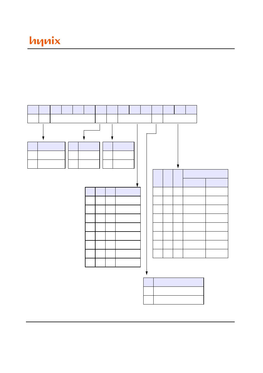
MODE REGISTER SET (MRS)
The mode register is used to store the various operating modes such as /CAS latency, addressing mode, burst length,
burst type, test mode, DLL reset. The mode register is programed via MRS command. This command is issued by the
low signals of /RAS, /CAS, /CS, /WE and BA0. This command can be issued only when all banks are in idle state and
CKE must be high at least one cycle before the Mode Register Set Command can be issued. Two cycles are required to
write the data in mode register. During the MRS cycle, any command cannot be issued. Once mode register field is
determined, the information will be held until resetted by another MRS command.
BA1
BA0
A12
A11
A10
A9
A8
A7
A6
A5
A4
A3
A2
A1
A0
0
0
RFU
DR
TM
CAS Latency
BT
Burst Length
A2
A1
A0
Burst Length
Sequential
Interleave
0
0
0
Reserved
Reserved
0
0
1
2
2
0
1
0
4
4
0
1
1
8
8
1
0
0
Reserved
Reserved
1
0
1
Reserved
Reserved
1
1
0
Reserved
Reserved
1
1
1
Reserved
Reserved
A3
Burst Type
0
Sequential
1
Interleave
A6
A5
A4
CAS Latency
0
0
0
Reserved
0
0
1
Reserved
0
1
0
2
0
1
1
3
1
0
0
Reserved
1
0
1
1.5
1
1
0
2.5
1
1
1
Reserved
A7
Test Mode
0
Normal
1
Test
A8
DLL Reset
0
No
1
Yes
BA0
MRS Type
0
MRS
1
EMRS
Rev. 0.1/Apr. 02 20
HY5DU56422A(L)F
HY5DU56822A(L)F
HY5DU561622A(L)F
BURST DEFINITION
BURST LENGTH & TYPE
Read and write accesses to the DDR SDRAM are burst oriented, with the burst length being programmable. The burst
length determines the maximum number of column locations that can be accessed for a given Read or Write com-
mand. Burst lengths of 2, 4, or 8 locations are available for both the sequential and the interleaved burst types.
Reserved states should not be used, as unknown operation or incompatibility with future versions may result.
When a Read or Write command is issued, a block of columns equal to the burst length is effectively selected. All
accesses for that burst take place within this block, meaning that the burst wraps within the block if a boundary is
reached. The block is uniquely selected by A1-Ai when the burst length is set to two, by A 2 -Ai when the burst length
is set to four and by A 3 -Ai when the burst length is set to eight (where Ai is the most significant column address bit
for a given configuration). The remaining (least significant) address bit(s) is (are) used to select the starting location
within the block. The programmed burst length applies to both Read and Write bursts.
Accesses within a given burst may be programmed to be either sequential or interleaved; this is referred to as the
burst type and is selected via bit A3. The ordering of accesses within a burst is determined by the burst length, the
burst type and the starting column address, as shown in Burst Definitionon Table
Burst Length
Starting Address (A2,A1,A0)
Sequential
Interleave
2
XX0
0, 1
0, 1
XX1
1, 0
1, 0
4
X00
0, 1, 2, 3
0, 1, 2, 3
X01
1, 2, 3, 0
1, 0, 3, 2
X10
2, 3, 0, 1
2, 3, 0, 1
X11
3, 0, 1, 2
3, 2, 1, 0
8
000
0, 1, 2, 3, 4, 5, 6, 7
0, 1, 2, 3, 4, 5, 6, 7
001
1, 2, 3, 4, 5, 6, 7, 0
1, 0, 3, 2, 5, 4, 7, 6
010
2, 3, 4, 5, 6, 7, 0, 1
2, 3, 0, 1, 6, 7, 4, 5
011
3, 4, 5, 6, 7, 0, 1, 2
3, 2, 1, 0, 7, 6, 5, 4
100
4, 5, 6, 7, 0, 1, 2, 3
4, 5, 6, 7, 0, 1, 2, 3
101
5, 6, 7, 0, 1, 2, 3, 4
5, 4, 7, 6, 1, 0, 3, 2
110
6, 7, 0, 1, 2, 3, 4, 5
6, 7, 4, 5, 2, 3, 0, 1
111
0, 1, 2, 3, 4, 5, 6, 7
7, 6, 5, 4, 3, 2, 1, 0

Rev. 0.1/Apr. 02 21
HY5DU56422A(L)F
HY5DU56822A(L)F
HY5DU561622A(L)F
CAS LATENCY
The Read latency, or CAS latency, is the delay, in clock cycles, between the registration of a Read command and the
availability of the first burst of output data. The latency can be programmed 1.5, 2, 2.5 or 3 clocks.
If a Read command is registered at clock edge n, and the latency is m clocks, the data is available nominally coincident
with clock edge n + m.
Reserved states should not be used as unknown operation or incompatibility with future versions may result.
DLL RESET
The DLL must be enabled for normal operation. DLL enable is required during power up initialization, and upon return-
ing to normal operation after having disabled the DLL for the purpose of debug or evaluation. The DLL is automatically
disabled when entering self refresh operation and is automatically re-enabled upon exit of self refresh operation. Any
time the DLL is enabled, 200 clock cycles must occur to allow time for the internal clock to lock to the externally
applied clock before an any command can be issued.
OUTPUT DRIVER IMPEDANCE CONTROL
The normal drive strength for all outputs is specified to be SSTL_2, Class II. Hynix also supports a half strength driver
option, intended for lighter load and/or point-to-point environments. Selection of the half strength driver option will
reduce the output drive strength by 50% of that of the full strength driver. I-V curves for both the full strength driver
and the half strength driver are included in this document.
Rev. 0.1/Apr. 02 22
HY5DU56422A(L)F
HY5DU56822A(L)F
HY5DU561622A(L)F
EXTENDED MODE REGISTER SET (EMRS)
The Extended Mode Register controls functions beyond those controlled by the Mode Register; these additional func-
tions include DLL enable/disable, output driver strength selection(optional). These functions are controlled via the bits
shown below. The Extended Mode Register is programmed via the Mode Register Set command ( BA0=1 and BA1=0)
and will retain the stored information until it is programmed again or the device loses power.
The Extended Mode Register must be loaded when all banks are idle and no bursts are in progress, and the controller
must wait the specified time before initiating any subsequent operation. Violating either of these requirements will
result in unspecified operation.
BA1
BA0
A12
A11
A10
A9
A8
A7
A6
A5
A4
A3
A2
A1
A0
0
1
RFU*
0**
DS
DLL
A0
DLL enable
0
Enable
1
Diable
BA0
MRS Type
0
MRS
1
EMRS
A1
Output Driver
Impedance Control
0
Full Strength Driver
1
Half Strength Driver
* All bits in RFU address fields must be programmed to Zero, all other states are reserved for future usage
** This part do not support /QFC function, A2 must be programmed to Zero.

Rev. 0.1/Apr. 02 23
HY5DU56422A(L)F
HY5DU56822A(L)F
HY5DU561622A(L)F
ABSOLUTE MAXIMUM RATINGS
Note : Operation at above absolute maximum rating can adversely affect device reliability
DC OPERATING CONDITIONS
(TA=0 to 70
o
C, Voltage referenced to V
SS
= 0V)
Note :
1. V
DDQ
must not exceed the level of V
DD
.
2. V
IL
(min) is acceptable -1.5V AC pulse width with < 5ns of duration.
3. V
REF
is expected to be equal to 0.5*V
DDQ
of the transmitting device, and to track variations in the dc level of the same.
Peak to peak noise on V
REF
may not exceed +/- 2% of the dc value.
DC CHARACTERISTICS I
(TA=0 to 70
�
C, Voltage referenced to V
SS
= 0V)
Note :
1. V
IN
=0 to V
DD
, All other pins are not tested under V
IN
=0V. 2. D
OUT
is disabled, V
OUT
=0 to V
DDQ
Parameter
Symbol
Rating
Unit
Ambient Temperature
T
A
0 ~ 70
o
C
Storage Temperature
T
STG
-55 ~ 125
o
C
Voltage on Any Pin relative to V
SS
V
IN
, V
OUT
-0.5 ~ 3.6
V
Voltage on V
DD
relative to V
SS
V
DD
-0.5 ~ 3.6
V
Voltage on V
DDQ
relative to V
SS
V
DDQ
-0.5 ~ 3.6
V
Output Short Circuit Current
I
OS
50
mA
Power Dissipation
P
D
1
W
Soldering Temperature
Time
T
SOLDER
260
10
o
C
sec
Parameter
Symbol
Min
Typ.
Max
Unit
Note
Power Supply Voltage
V
DD
2.3
2.5
2.7
V
Power Supply Voltage
V
DDQ
2.3
2.5
2.7
V
1
Input High Voltage
V
IH
V
REF
+ 0.15
-
V
DDQ
+ 0.3
V
Input Low Voltage
V
IL
-0.3
-
V
REF
- 0.15
V
2
Termination Voltage
V
TT
V
REF
- 0.04
V
REF
V
REF
+ 0.04
V
Reference Voltage
V
REF
VDDQ/2 -
50mV
VDDQ/2
VDDQ/2 +
50mV
V
3
Parameter
Symbol
Min.
Max
Unit
Note
Input Leakage Current
I
LI
-2
2
uA
1
Output Leakage Current
I
LO
-5
5
uA
2
Output High Voltage
V
OH
V
TT
+ 0.76
-
V
I
OH
= -15.2mA
Output Low Voltage
V
OL
-
V
TT
- 0.76
V
I
OL
= +15.2mA

Rev. 0.1/Apr. 02 24
HY5DU56422A(L)F
HY5DU56822A(L)F
HY5DU561622A(L)F
DC CHARACTERISTICS II
(TA=0 to 70
o
C, Voltage referenced to V
SS
= 0V)
64Mx4
Parameter
Symbol
Test Condition
Speed
Unit Note
-J
-M
-K
-H
-L
Operating Current
IDD0
One bank; Active - Precharge;
tRC=tRC(min); tCK=tCK(min); DQ,DM and
DQS inputs changing twice per clock cycle;
address and control inputs changing once
per clock cycle
105
95
90
mA
Operating Current
I
DD1
One bank; Active - Read - Precharge;
Burst=2; tRC=tRC(min); tCK=tCK(min);
address and control inputs changing once
per clock cycle; IOUT=0mA
150
130
120
mA
Precharge Power
Down Standby
Current
I
DD2P
All banks idle; Power down mode; CKE=Low,
tCK=tCK(min)
20
mA
Idle Standby Current
I
DD2F
/CS=High, All banks idle; tCK=tCK(min);
CKE=High; address and control inputs
changing once per clock cycle.
VIN=VREF for DQ, DQS and DM
50
40
35
mA
Active Power Down
Standby Current
I
DD3P
One bank active; Power down mode ;
CKE=Low, tCK=tCK(min)
25
mA
Active Standby
Current
I
DD3N
/CS=HIGH; CKE=HIGH; One bank; Active-
Precharge; tRC=tRAS(max); tCK=tCK(min);
DQ, DM and DQS inputs changing twice per
clock cycle; Address and other control inputs
changing once per clock cycle
60
50
50
mA
Operating Current
I
DD4R
Burst=2; Reads; Continuous burst; One bank
active; Address and control inputs changing
once per clock cycle; tCK=tCK(min);
IOUT=0mA
280
240
180
mA
Operating Current
I
DD4W
Burst=2; Writes; Continuous burst; One
bank active; Address and control inputs
changing once per clock cycle;
tCK=tCK(min); DQ, DM and DQS inputs
changing twice per clock cycle
280
240
180
mA
Auto Refresh Current
I
DD5
tRC=tRFC(min); All banks active
230
210
195
mA
Self Refresh Current
I
DD6
CKE=<0.2V; External clock on;
tCK=tCK(min)
Normal
3
mA
Low Power
1.5
mA
Operating Current -
Four Bank Operation
I
DD7
Four bank interleaving with BL=4, Refer to
the following page for detailed test condition
305
295
295
mA

Rev. 0.1/Apr. 02 25
HY5DU56422A(L)F
HY5DU56822A(L)F
HY5DU561622A(L)F
DC CHARACTERISTICS II
(TA=0 to 70
o
C, Voltage referenced to V
SS
= 0V)
32Mx8
Parameter
Symbol
Test Condition
Speed
Unit Note
-J
-M
-K
-H
-L
Operating Current
IDD0
One bank; Active - Precharge;
tRC=tRC(min); tCK=tCK(min); DQ,DM and
DQS inputs changing twice per clock cycle;
address and control inputs changing once
per clock cycle
105
95
90
mA
Operating Current
I
DD1
One bank; Active - Read - Precharge;
Burst=2; tRC=tRC(min); tCK=tCK(min);
address and control inputs changing once
per clock cycle; IOUT=0mA
150
130
120
mA
Precharge Power
Down Standby
Current
I
DD2P
All banks idle; Power down mode; CKE=Low,
tCK=tCK(min)
20
mA
Idle Standby Current
I
DD2F
/CS=High, All banks idle; tCK=tCK(min);
CKE=High; address and control inputs
changing once per clock cycle.
VIN=VREF for DQ, DQS and DM
50
40
35
mA
Active Power Down
Standby Current
I
DD3P
One bank active; Power down mode ;
CKE=Low, tCK=tCK(min)
25
mA
Active Standby
Current
I
DD3N
/CS=HIGH; CKE=HIGH; One bank; Active-
Precharge; tRC=tRAS(max); tCK=tCK(min);
DQ, DM and DQS inputs changing twice per
clock cycle; Address and other control inputs
changing once per clock cycle
60
50
50
mA
Operating Current
I
DD4R
Burst=2; Reads; Continuous burst; One bank
active; Address and control inputs changing
once per clock cycle; tCK=tCK(min);
IOUT=0mA
290
250
190
mA
Operating Current
I
DD4W
Burst=2; Writes; Continuous burst; One
bank active; Address and control inputs
changing once per clock cycle;
tCK=tCK(min); DQ, DM and DQS inputs
changing twice per clock cycle
290
250
190
mA
Auto Refresh Current
I
DD5
tRC=tRFC(min); All banks active
230
210
195
mA
Self Refresh Current
I
DD6
CKE=<0.2V; External clock on;
tCK=tCK(min)
Normal
3
mA
Low Power
1.5
mA
Operating Current -
Four Bank Operation
I
DD7
Four bank interleaving with BL=4, Refer to
the following page for detailed test condition
315
305
280
mA
Rev. 0.1/Apr. 02 26
HY5DU56422A(L)F
HY5DU56822A(L)F
HY5DU561622A(L)F
DC CHARACTERISTICS II
(TA=0 to 70
o
C, Voltage referenced to V
SS
= 0V)
16Mx16
Parameter
Symbol
Test Condition
Speed
Unit Note
-J
-M
-K
-H
-L
Operating Current
IDD0
One bank; Active - Precharge;
tRC=tRC(min); tCK=tCK(min); DQ,DM and
DQS inputs changing twice per clock cycle;
address and control inputs changing once
per clock cycle
105
95
90
mA
Operating Current
I
DD1
One bank; Active - Read - Precharge;
Burst=2; tRC=tRC(min); tCK=tCK(min);
address and control inputs changing once
per clock cycle; IOUT=0mA
150
130
120
mA
Precharge Power
Down Standby
Current
I
DD2P
All banks idle; Power down mode; CKE=Low,
tCK=tCK(min)
20
mA
Idle Standby Current
I
DD2F
/CS=High, All banks idle; tCK=tCK(min);
CKE=High; address and control inputs
changing once per clock cycle.
VIN=VREF for DQ, DQS and DM
50
40
35
mA
Active Power Down
Standby Current
I
DD3P
One bank active; Power down mode ;
CKE=Low, tCK=tCK(min)
25
mA
Active Standby
Current
I
DD3N
/CS=HIGH; CKE=HIGH; One bank; Active-
Precharge; tRC=tRAS(max); tCK=tCK(min);
DQ, DM and DQS inputs changing twice per
clock cycle; Address and other control inputs
changing once per clock cycle
60
50
50
mA
Operating Current
I
DD4R
Burst=2; Reads; Continuous burst; One bank
active; Address and control inputs changing
once per clock cycle; tCK=tCK(min);
IOUT=0mA
290
250
190
mA
Operating Current
I
DD4W
Burst=2; Writes; Continuous burst; One
bank active; Address and control inputs
changing once per clock cycle;
tCK=tCK(min); DQ, DM and DQS inputs
changing twice per clock cycle
290
250
190
mA
Auto Refresh Current
I
DD5
tRC=tRFC(min); All banks active
230
210
195
mA
Self Refresh Current
I
DD6
CKE=<0.2V; External clock on;
tCK=tCK(min)
Normal
3
mA
Low Power
1.5
mA
Operating Current -
Four Bank Operation
I
DD7
Four bank interleaving with BL=4, Refer to
the following page for detailed test condition
335
325
290
mA

Rev. 0.1/Apr. 02 27
HY5DU56422A(L)F
HY5DU56822A(L)F
HY5DU561622A(L)F
DETAILED TEST CONDITIONS FOR DDR SDRAM IDD1 & IDD7
IDD1 : Operating current: One bank operation
1. Only one bank is accessed with tRC(min), Burst Mode, Address and Control inputs on NOP edge are
changing once per clock cycle. lout = 0mA
2. Timing patterns
- DDR200(100Mhz, CL=2) : tCK = 10ns, CL2, BL=2, tRCD = 2*tCK, tRC = 10*tCK, tRAS = 5*tCK
Read : A0 N R0 N N P0 N A0 N - repeat the same timing with random address changing
50% of data changing at every burst
- DDR266B(133Mhz, CL=2.5) : tCK = 7.5ns, CL=2.5, BL=2, tRCD = 3*tCK, tRC = 9*tCK, tRAS = 6*tCK
Read : A0 N N R0 N N P0 N N A0 N - repeat the same timing with random address changing
50% of data changing at every burst
- DDR266A(133Mhz, CL=2) : tCK = 7.5ns, CL=2, BL=2, tRCD = 3*tCK, tRC = 9*tCK, tRAS = 6*tCK
Read : A0 N N R0 N N P0 N N A0 N - repeat the same timing with random address changing
50% of data changing at every burst
- DDR266(133Mhz, CL=2) : tCK = 7.5ns, CL=2, BL=2, tRCD = 2*tCK, tRC = 8*tCK, tRAS = 6*tCK
Read : A0 N R0 N N N P0 N A0 N - repeat the same timing with random address changing
50% of data changing at every burst
- DDR333(166Mhz, CL=2.5) : tCK = 6ns, CL=2, BL=2, tRCD = 3*tCK, tRC = 10*tCK, tRAS = 7*tCK
Read : A0 N N R0 N N N P0 N N A0 N - repeat the same timing with random address changing
50% of data changing at every burst
Legend : A=Activate, R=Read, W=Write, P=Precharge, N=NOP
IDD7 : Operating current: Four bank operation
1. Four banks are being interleaved with tRC(min), Burst Mode, Address and Control inputs on NOP edge are not
changing. lout = 0mA
2. Timing patterns
- DDR200(100Mhz, CL=2) : tCK = 10ns, CL2, BL=4, tRRD = 2*tCK, tRCD= 3*tCK, Read with autoprecharge
Read : A0 N A1 R0 A2 R1 A3 R2 A0 R3 A1 R0 - repeat the same timing with random address changing
50% of data changing at every burst
- DDR266B(133Mhz, CL=2.5) : tCK = 7.5ns, CL=2.5, BL=4, tRRD = 2*tCK, tRCD = 3*tCK, Read with autoprecharge
Read : A0 N A1 R0 A2 R1 A3 R2 N R3 A0 N A1 R0 - repeat the same timing with random address changing
50% of data changing at every burst
- DDR266A(133Mhz, CL=2) : tCK = 7.5ns, CL2=2, BL=4, tRRD = 2*tCK, tRCD = 3*tCK, Read with autoprecharge
Read : A0 N A1 R0 A2 R1 A3 R2 N R3 A0 N A1 R0 - repeat the same timing with random address changing
50% of data changing at every burst
- DDR333(166Mhz, CL=2.5) : tCK = 6ns, CL=2.5, BL=4, tRRD = 2*tCK, tRCD = 3*tCK, Read with autoprecharge
Read : A0 N A1 R0 A2 R1 A3 R2 N R3 A0 N A1 R0 - repeat the same timing with random address changing
50% of data changing at every burst
Legend : A=Activate, R=Read, W=Write, P=Precharge, N=NOP
Rev. 0.1/Apr. 02 28
HY5DU56422A(L)F
HY5DU56822A(L)F
HY5DU561622A(L)F
AC OPERATING CONDITIONS
(TA=0 to 70
o
C, Voltage referenced to V
SS
= 0V)
Note :
1. VID is the magnitude of the difference between the input level on CK and the input on /CK.
2. The value of VIX is expected to equal 0.5*V DDQ of the transmitting device and must track variations in the DC level of the same.
AC OPERATING TEST CONDITIONS
(TA=0 to 70
o
C, Voltage referenced to VSS = 0V)
Parameter
Symbol
Min
Max
Unit
Note
Input High (Logic 1) Voltage, DQ, DQS and DM signals
V
IH(AC)
V
REF
+ 0.31
V
Input Low (Logic 0) Voltage, DQ, DQS and DM signals
V
IL(AC)
V
REF
- 0.31
V
Input Differential Voltage, CK and /CK inputs
V
ID(AC)
0.7
V
DDQ
+ 0.6
V
1
Input Crossing Point Voltage, CK and /CK inputs
V
IX(AC)
0.5*V
DDQ
-0.2
0.5*V
DDQ
+0.2
V
2
Parameter
Value
Unit
Reference Voltage
V
DDQ
x 0.5
V
Termination Voltage
V
DDQ
x 0.5
V
AC Input High Level Voltage (V
IH
, min)
V
REF
+ 0.31
V
AC Input Low Level Voltage (V
IL
, max)
V
REF
- 0.31
V
Input Timing Measurement Reference Level Voltage
V
REF
V
Output Timing Measurement Reference Level Voltage
V
TT
V
Input Signal maximum peak swing
1.5
V
Input minimum Signal Slew Rate
1
V/ns
Termination Resistor (R
T
)
50
Series Resistor (R
S
)
25
Output Load Capacitance for Access Time Measurement (C
L
)
30
pF
Rev. 0.1/Apr. 02 29
HY5DU56422A(L)F
HY5DU56822A(L)F
HY5DU561622A(L)F
AC CHARACTERISTICS I
(AC operating conditions unless otherwise noted)
Parameter
Symbol
DDR333
DDR266
Unit
Note
Min
Max
Min
Max
Row Cycle Time
tRC
60
-
60
-
ns
Auto Refresh Row Cycle Time
tRFC
72
-
75
-
ns
Row Active Time
tRAS
42
70K
45
120K
ns
Active to Read with Auto Precharge Delay
tRAP
tRCD or
tRPmin
-
tRCD or
tRPmin
-
ns
16
Row Address to Column Address Delay
tRCD
18
-
15
-
ns
Row Active to Row Active Delay
tRRD
12
-
15
-
ns
Column Address to Column Address Delay
tCCD
1
-
1
-
CK
Row Precharge Time
tRP
18
-
15
-
ns
Write Recovery Time
tWR
15
-
15
-
ns
Write to Read Command Delay
tWTR
1
-
1
-
CK
Auto Precharge Write Recovery + Precharge Time
tDAL
(tWR/tCK)
+
(tRP/tCK)
-
(tWR/tCK)
+
(tRP/tCK)
-
CK
15
System Clock Cycle Time
CL = 2.5
tCK
6
12
7.5
12
ns
CL = 2
7.5
12
7.5
12
ns
Clock High Level Width
tCH
0.45
0.55
0.45
0.55
CK
Clock Low Level Width
tCL
0.45
0.55
0.45
0.55
CK
Data-Out edge to Clock edge Skew
tAC
-0.7
0.7
-0.75
0.75
ns
DQS-Out edge to Clock edge Skew
tDQSCK
-0.6
0.6
-0.75
0.75
ns
DQS-Out edge to Data-Out edge Skew
tDQSQ
-
0.4
-
0.5
ns
Data-Out hold time from DQS
tQH
t
HP
-t
QHS
-
t
HP
-t
QHS
-
ns
1,10
Clock Half Period
tHP
min
(tCL,tCH)
-
min
(tCL,tCH)
-
ns
1,9
Data Hold Skew Factor
tQHS
-
0.6
-
0.75
ns
10
Valid Data Output Window
tDV
t
QH
-t
DQSQ
t
QH
-t
DQSQ
ns
Data-out high-impedance window from CK,/CK
tHZ
-0.7
0.7
-0.75
0.75
ns
17
Data-out low-impedance window from CK, /CK
tLZ
-0.7
0.7
-0.75
0.75
ns
Input Setup Time (fast slew rate)
tIS
0.75
-
0.9
-
ns
2,3,5,6
Input Hold Time (fast slew rate)
tIH
0.75
-
0.9
-
ns
Rev. 0.1/Apr. 02 30
HY5DU56422A(L)F
HY5DU56822A(L)F
HY5DU561622A(L)F
Input Setup Time (slow slew rate)
t
IS
0.8
-
1.0
-
ns
2,4,5,6
Input Hold Time (slow slew rate)
t
IH
0.8
-
1.0
-
ns
Input Pulse Width
t
IPW
2.2
-
2.2
-
ns
6
Write DQS High Level Width
t
DQSH
0.35
-
0.35
-
CK
Write DQS Low Level Width
t
DQSL
0.35
-
0.35
-
CK
Clock to First Rising edge of DQS-In
t
DQSS
0.75
1.25
0.72
1.28
CK
Data-In Setup Time to DQS-In (DQ & DM)
t
DS
0.45
-
0.5
-
ns
6,7,11,
12,13
Data-in Hold Time to DQS-In (DQ & DM)
t
DH
0.45
-
0.5
-
ns
DQ & DM Input Pulse Width
t
DIPW
1.75
-
1.75
-
ns
Read DQS Preamble Time
t
RPRE
0.9
1.1
0.9
1.1
CK
Read DQS Postamble Time
t
RPST
0.4
0.6
0.4
0.6
CK
Write DQS Preamble Setup Time
t
WPRES
0
-
0
-
CK
Write DQS Preamble Hold Time
t
WPREH
0.25
-
0.25
-
CK
Write DQS Postamble Time
t
WPST
0.4
0.6
0.4
0.6
CK
Mode Register Set Delay
t
MRD
2
-
2
-
CK
Exit Self Refresh to Any Execute Command
t
XSC
200
-
200
-
CK
8
Average Periodic Refresh Interval
t
REFI
-
7.8
-
7.8
us
Parameter
Symbol
DDR333
DDR266
Unit
Note
Min
Max
Min
Max
Rev. 0.1/Apr. 02 31
HY5DU56422A(L)F
HY5DU56822A(L)F
HY5DU561622A(L)F
AC CHARACTERISTICS II
(AC operating conditions unless otherwise noted)
Parameter
Symbol
DDR266A
DDR266B
DDR200
Unit Note
Min
Max
Min
Max
Min
Max
Row Cycle Time
tRC
65
-
65
-
70
-
ns
Auto Refresh Row Cycle Time
tRFC
75
-
75
-
80
-
ns
Row Active Time
tRAS
45
120K
45
120K
50
120K
ns
Active to Read with Auto Precharge Delay
tRAP
tRCD or
tRPmin
-
tRCD or
tRPmin
-
tRCD or
tRPmin
-
ns
16
Row Address to Column Address Delay
tRCD
20
-
20
-
20
-
ns
Row Active to Row Active Delay
tRRD
15
-
15
-
15
-
ns
Column Address to Column Address Delay
tCCD
1
-
1
-
1
-
CK
Row Precharge Time
tRP
20
-
20
-
20
-
ns
Write Recovery Time
tWR
15
-
15
-
15
-
ns
Write to Read Command Delay
tWTR
1
-
1
-
1
-
CK
Auto Precharge Write Recovery +
Precharge Time
tDAL
(tWR/tCK)
+
(tRP/tCK)
-
(tWR/tCK)
+
(tRP/tCK)
-
(tWR/tCK)
+
(tRP/tCK)
-
CK
15
System Clock Cycle Time
CL = 2.5
tCK
7.5
12
7.5
12
8.0
12
ns
CL = 2
7.5
12
10
12
10
12
ns
Clock High Level Width
tCH
0.45
0.55
0.45
0.55
0.45
0.55
CK
Clock Low Level Width
tCL
0.45
0.55
0.45
0.55
0.45
0.55
CK
Data-Out edge to Clock edge Skew
tAC
-0.75
0.75
-0.75
0.75
-0.75
0.75
ns
DQS-Out edge to Clock edge Skew
tDQSCK
-0.75
0.75
-0.75
0.75
-0.75
0.75
ns
DQS-Out edge to Data-Out edge Skew
tDQSQ
-
0.5
-
0.5
-
0.6
ns
Data-Out hold time from DQS
tQH
t
HP
-t
QHS
-
t
HP
-t
QHS
-
t
HP
-t
QHS
-
ns
1,10
Clock Half Period
tHP
min
(tCL,tCH)
-
min
(tCL,tCH)
-
min
(tCL,tCH)
-
ns
1,9
Data Hold Skew Factor
tQHS
-
0.75
-
0.75
-
0.75
ns
10
Valid Data Output Window
tDV
t
QH
-t
DQSQ
t
QH
-t
DQSQ
t
QH
-t
DQSQ
ns
Data-out high-impedance window from
CK,/CK
tHZ
-0.75
0.75
-0.75
0.75
-0.8
0.8
ns
17
Data-out low-impedance window from
CK, /CK
tLZ
-0.75
0.75
-0.75
0.75
-0.8
0.8
ns
17
Rev. 0.1/Apr. 02 32
HY5DU56422A(L)F
HY5DU56822A(L)F
HY5DU561622A(L)F
Input Setup Time (fast slew rate)
t
IS
0.9
-
0.9
-
1.1
-
ns
2,3,5,
6
Input Hold Time (fast slew rate)
t
IH
0.9
-
0.9
-
1.1
-
ns
Input Setup Time (slow slew rate)
t
IS
1.0
-
1.0
-
1.1
-
ns
2,4,5,
6
Input Hold Time (slow slew rate)
t
IH
1.0
-
1.0
-
1.1
-
ns
Input Pulse Width
t
IPW
2.2
-
2.2
-
2.5
-
ns
6
Write DQS High Level Width
t
DQSH
0.35
-
0.35
-
0.35
-
CK
Write DQS Low Level Width
t
DQSL
0.35
-
0.35
-
0.35
-
CK
Clock to First Rising edge of DQS-In
t
DQSS
0.75
1.25
0.75
1.25
0.75
1.25
CK
Data-In Setup Time to DQS-In (DQ & DM)
t
DS
0.5
-
0.5
-
0.6
-
ns
6,7,
11,12
,13
Data-in Hold Time to DQS-In (DQ & DM)
t
DH
0.5
-
0.5
-
0.6
-
ns
DQ & DM Input Pulse Width
t
DIPW
1.75
-
1.75
-
2
-
ns
Read DQS Preamble Time
t
RPRE
0.9
1.1
0.9
1.1
0.9
1.1
CK
Read DQS Postamble Time
t
RPST
0.4
0.6
0.4
0.6
0.4
0.6
CK
Write DQS Preamble Setup Time
t
WPRES
0
-
0
-
0
-
CK
Write DQS Preamble Hold Time
t
WPREH
0.25
-
0.25
-
0.25
-
CK
Write DQS Postamble Time
t
WPST
0.4
0.6
0.4
0.6
0.4
0.6
CK
Mode Register Set Delay
t
MRD
2
-
2
-
2
-
CK
Exit Self Refresh to Any Execute Command
t
XSC
200
-
200
-
200
-
CK
8
Average Periodic Refresh Interval
t
REFI
-
7.8
-
7.8
-
7.8
us
Parameter
Symbol
DDR266A
DDR266B
DDR200
Unit Note
Min
Max
Min
Max
Min
Max

Rev. 0.1/Apr. 02 33
HY5DU56422A(L)F
HY5DU56822A(L)F
HY5DU561622A(L)F
Note :
1.
This calculation accounts for tDQSQ(max), the pulse width distortion of on-chip circuit and jitter.
2.
Data sampled at the rising edges of the clock : A0~A12, BA0~BA1, CKE, /CS, /RAS, /CAS, /WE.
3.
For command/address input slew rate>=1.0V/ns
4.
For command/address input slew rate>=0.5V/ns and <1.0V/ns
This derating table is used to increase tIS/tIH in case where the input slew-rate is below 0.5V/ns.
Input Setup / Hold Slew-rate Derating Table.
5.
CK, /CK slew rates are>=1.0V/ns
6.
These parameters guarantee device timing, but they are not necessarily tested on each device, and they may be guaranteed by
design or tester correlation.
7.
Data latched at both rising and falling edges of Data Strobes(LDQS/UDQS) : DQ, LDM/UDM.
8.
Minimum of 200 cycles of stable input clocks after Self Refresh Exit command, where CKE is held high, is required to complete
Self Refresh Exit and lock the internal DLL circuit of DDR SDRAM.
9.
Min (tCL, tCH) refers to the smaller of the actual clock low time and the actual clock high time as provided to the device (i.e. this
value can be greater than the minimum specification limits for tCL and tCH).
10. tHP = minimum half clock period for any given cycle and is defined by clock high or clock low (tCH, tCL). tQHS consists of
tDQSQmax, the pulse width distortion of on-chip clock circuits, data pin to pin skew and output pattern effects and p-channel to
n-channel variation of the output drivers.
11. This derating table is used to increase tDS/tDH in case where the input slew-rate is below 0.5V/ns.
Input Setup / Hold Slew-rate Derating Table.
12. I/O Setup/Hold Plateau Derating. This derating table is used to increase tDS/tDH in case where the input level is flat below VREF
+/-310mV for a duration of up to 2ns.
13. I/O Setup/Hold Delta Inverse Slew Rate Derating. This derating table is used to increase tDS/tDH in case where the DQ and
DQS slew rates differ. The Delta Inverse Slew Rate is calculated as (1/SlewRate1)-(1/SlewRate2). For example, if slew rate 1=
0.5V/ns and Slew Rate2=0.4V/n then the Delta Inverse Slew Rate=-0.5ns/V.
Input Setup / Hold Slew-rate
Delta tIS
Delta tIH
V/ns
ps
ps
0.5
0
0
0.4
+50
0
0.3
+100
0
Input Setup / Hold Slew-rate
Delta tDS
Delta tDH
V/ns
ps
ps
0.5
0
0
0.4
+75
+75
0.3
+150
+150
I/O Input Level
Delta tDS
Delta tDH
mV
ps
ps
+280
+50
+50
(1/SlewRate1)-(1/SlewRate2)
Delta tDS
Delta tDH
ns/V
ps
ps
0
0
0
+/-0.25
+50
+50
+/- 0.5
+100
+100

Rev. 0.1/Apr. 02 34
HY5DU56422A(L)F
HY5DU56822A(L)F
HY5DU561622A(L)F
14. DQS, DM and DQ input slew rate is specified to prevent double clocking of data and preserve setup and hold times. Signal
transitions through the DC region must be monotonic.
15. tDAL = (tDPL / tCK ) + (tRP / tCK ). For each of the terms above, if not already an integer, round to the next highest integer.
tCK is equal to the actual system clock cycle time.
Example: For DDR266B at CL=2.5 and tCK = 7.5 ns,
tDAL = (15 ns / 7.5 ns) + (20 ns / 7.5 ns) = (2.00) + (2.67)
Round up each non-integer to the next highest integer: = (2) + (3), tDAL = 5 clocks
16. For the parts which do not has internal RAS lockout circuit, Active to Read with Auto precharge delay should be
tRAS - (BL/2) x tCK.
17. tHZ and tLZ transitions occur in the same access time windows as valid data trasitions. These parameters are not referenced
to a specific voltage level but specify when the device output is no longer driving (HZ), or begins driving (LZ).
Rev. 0.1/Apr. 02 35
HY5DU56422A(L)F
HY5DU56822A(L)F
HY5DU561622A(L)F
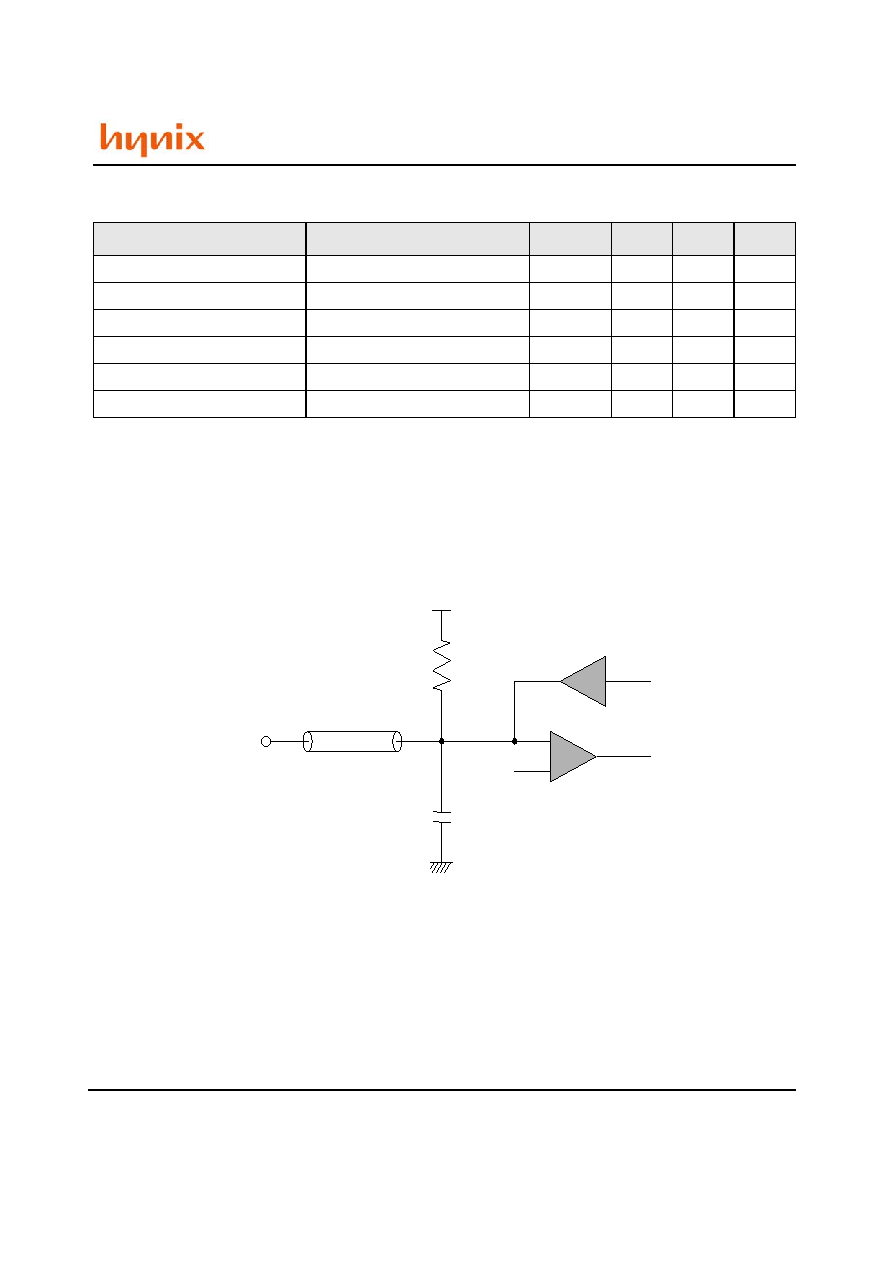
CAPACITANCE
(T
A
=25
o
C, f=100MHz )
Note :
1. VDD = min. to max., VDDQ = 2.3V to 2.7V, V
O
DC = VDDQ/2, V
O
peak-to-peak = 0.2V
2. Pins not under test are tied to GND.
3. These values are guaranteed by design and are tested on a sample basis only.
OUTPUT LOAD CIRCUIT
Parameter
Pin
Symbol
Min
Max
Unit
Input Clock Capacitance
CK, /CK
C
I1
1.5
2.5
pF
Delta Input Clock Capacitance
CK, /CK
Delta C
I1
-
0.25
pF
Input Capacitance
All other input-only pins
C
I1
1.5
2.5
pF
Delta Input Capacitance
All other input-only pins
Delta C
I2
-
0.5
pF
Input / Output Capacitance
DQ, DQS, DM
C
IO
3.5
4.5
pF
Delta Input / Output Capacitance
DQ, DQS, DM
Delta C
IO
-
0.5
pF
V
REF
V
TT
R
T
=50
Zo=50
C
L
=30pF
Output

Rev. 0.1/Apr. 02 36
HY5DU56422A(L)F
HY5DU56822A(L)F
HY5DU561622A(L)F
PACKAGE INFORMATION