HY5DU56422
4 Banks x 16M x 4Bit Double Data Rate SDRAM
This document is a general product description and is subject to change without notice. Hyundai Electronics does not assume any
responsibility for use of circuits described. No patent licenses are implied.
Rev. 0.1/Mar.00
DESCRIPTION
The Hyundai HY5DU56422 is a 268,435,456-bit CMOS Double Data Rate(DDR) Synchronous DRAM, ideally suited
for the main memory applications which require large memory density and high bandwidth. HY5DU56422 is organized
as 4 banks of 16,777,216x4.
HY5DU56422 offers fully synchronous operations referenced to both rising and falling edges of the clock. While all
addresses and control inputs are latched on the rising edges of the clock(falling edges of the CLK), Data(DQ), Data
strobes(DQS) and Write data masks(DM) inputs are sampled on both rising and falling edges of it. The data paths are
internally pipelined and 2-bit prefetched to achieve very high bandwidth. All input and output voltage levels are compat-
ible with SSTL_2.
Mode register set options include the length of pipeline (CAS latency of 2 / 2.5 / 3), the number of consecutive read or
write cycles initiated by a single control command (Burst length of 2 / 4 / 8), the burst count sequence(sequential or
interleave), DQ FET Control (/QFC) and Output Driver types (Full / Half Strength Driver). Because data rate is doubled
through reading and writing at both rising and falling edges of the clock, 2X higher data bandwidth can be achieved
than that of traditional (single data rate) Synchronous DRAM.
FEATURES
∑
2.5V V
DD
and V
DDQ
power supply
∑
All inputs and outputs are compatible with SSTL_2
interface
∑
JEDEC standard 400mil 66pin TSOP-II with 0.65mm
pin pitch
∑
Fully differential clock operations(CLK & CLK) with
125MHz/133MHz/143MHz
∑
All addresses and control inputs except Data, Data
strobes and Data masks latched on the rising edges
of the clock
∑
Data(DQ) and Write masks(DM) latched on both ris-
ing and falling edges of the Data Stobe
∑
Data outputs on DQS edges when read (edged DQ)
Data inputs on DQS centers when write (centered
DQ)
∑
Delay Locked Loop(DLL) installed with DLL reset
mode
∑
Write mask byte controlled by DM
∑
Programmable CAS Latency 2 / 2.5 / 3 supported
∑
Write Operations with 1 Clock Write Latency
∑
/QFC & Half Strength Driver controlled by EMRS
∑
Programmable Burst Length 2 / 4 / 8 with both
sequential and interleave mode
∑
Internal four banks operation with single pulsed RAS
∑
Auto refresh and self refresh supported
∑
8092 refresh cycles / 64ms
ORDERING INFORMATION
Part No.
Power Suppy
Clock Frequency
Organization
Interface
Package
HY5DU56422(L)T-K
V
DD
=2.5V
V
DDQ
=2.5V
143MHz (*PC266A)
4Banks
x 16Mbit x 4
SSTL_2
400mil 66pin
TSOP II
HY5DU56422(L)T-H
133MHz (*PC266B)
HY5DU56422(L)T-L
125MHz (*PC200)
PRELIMINARY
* JEDEC Standard compliant
HY5DU56422
Rev. 0.1/Mar.00
2
400mil X 875mil
66 Pin TSOP-II
0.65mm Pin Pitch
TOP VIEW
V
DD
NC
V
DDQ
NC
DQ0
V
SSQ
NC
NC
V
DDQ
NC
DQ1
V
SSQ
NC
NC
V
DDQ
NC
NC
V
DD
/QFC, NC
NC
/WE
/CAS
/RAS
/CS
NC
BA0
BA1
A10/AP
A0
A1
A2
A3
V
DD
V
SS
NC
V
SSQ
NC
DQ3
V
DDQ
NC
NC
V
SSQ
NC
DQ2
V
DDQ
NC
NC
V
SSQ
DQS
NC
V
REF
V
SS
DM
/CLK
CLK
CKE
NC
A12
A11
A9
A8
A7
A6
A5
A4
V
SS
1
2
3
4
5
6
7
8
9
10
11
12
13
14
15
16
17
18
19
20
21
22
23
24
25
26
27
28
29
30
31
32
33
66
65
64
63
62
61
60
59
58
57
56
55
54
53
52
51
50
49
48
47
46
45
44
43
42
41
40
39
38
37
36
35
34
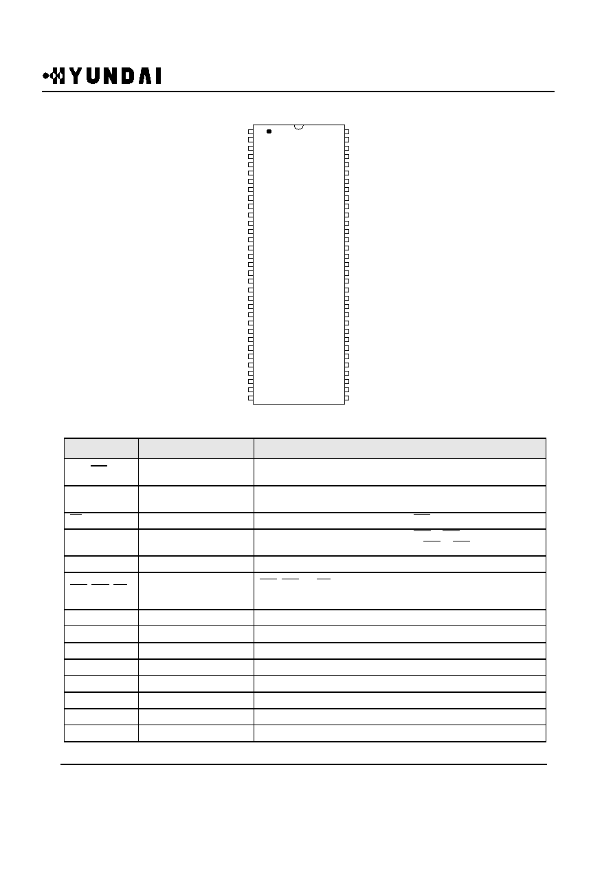
PIN CONFIGURATION
PIN DESCRIPTION
PIN
PIN NAME
DESCRIPTION
CLK, CLK
Differential Clock Input
The system clock input. All of the inputs are latched on the rising edges of the
clock except DQ, DQS and DM that are sampled on the both.
CKE
Clock Enable
Controls internal clock signal. When deactivated, the DDR SDRAM will be
one of the states among power down or self refresh.
CS
Chip Select
Enables or disables all inputs except CLK/CLK, CKE, DQS and DM.
BA0, BA1
Bank Select Address
Selects bank to be activated during either RAS or CAS activity.
Selects bank to be read/written during either RAS or CAS activity.
A0 ~ A12
Address
Row Address : A0 ~ A12, Column Address : A0 ~ A9,A11 AP Flag : A10
RAS, CAS, WE
Row Address Strobe,
Column Address Strobe,
Write Enable
RAS, CAS and WE define the operations.
Refer function truth table for details.
DM
Write Mask
Masks input data in write mode.
DQS
Data Input/Output Strobe
Active on the both edges for Data Input and Output.
DQ0 ~ DQ3
Data Input/Output
Multiplexed Data input / output pin.
V
DD
/V
SS
Power Supply/Ground
Power supply for internal circuits and input buffers.
V
DDQ
/V
SSQ
Data Output Power/Ground
Power supply for output buffers for Noise immunity.
V
REF
Reference Voltage
Reference voltage for inputs for SSTL interface.
/QFC (optional)
DQ FET Switch Control
Controls FET Switches on DQs used for reduction of impedance.
NC
No Connection
No connection.
HY5DU56422
Rev. 0.1/Mar.00
3
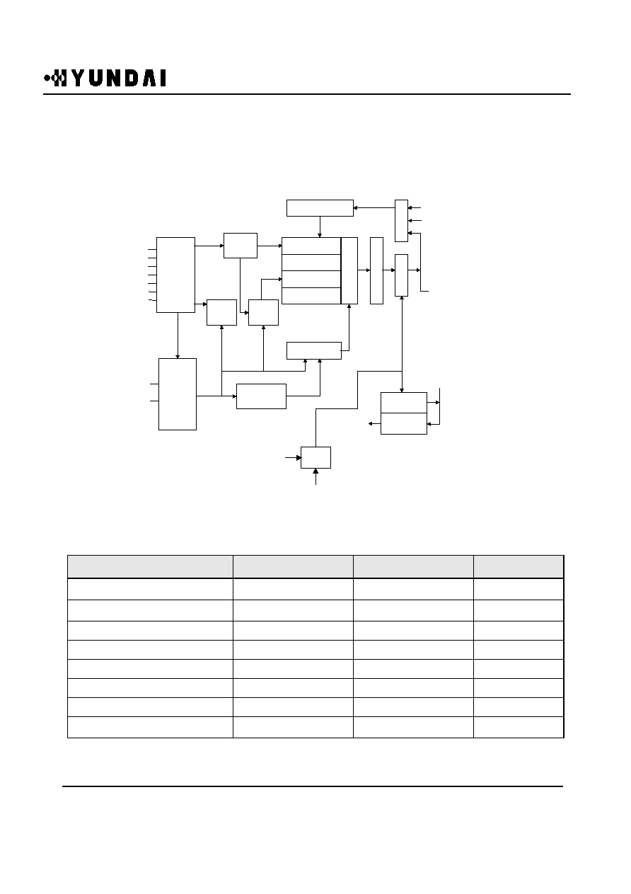
FUNCTIONAL BLOCK DIAGRAM
4banks x 16Mbit x 4 I/O Double data rate Synchronous DRAM
ABSOLUTE MAXIMUM RATINGS
Note : Operation at above absolute maximum rating can adversely affect device reliability.
Parameter
Symbol
Rating
Unit
Ambient Temperature
T
A
0 ~ 70
o
C
Storage Temperature
T
STG
-55 ~ 125
o
C
Voltage on Any Pin relative to V
SS
V
IN
, V
OUT
-0.5 ~ 3.6
V
Voltage on V
DD
relative to V
SS
V
DD
-0.5 ~ 3.6
V
Voltage on V
DDQ
relative to V
SS
V
DDQ
-0.5 ~ 3.6
V
Output Short Circuit Current
I
OS
50
mA
Power Dissipation
P
D
1
W
Soldering Temperature
Time
T
SOLDER
260
10
o
C
Sec
Command
Decoder
CLK
/CLK
CKE
/CS
/RAS
/CAS
/WE
Address
Buffer
ADD
Bank
Control
8Mx8 / Bank0
Column Decoder
Column Address
Counter
Sense AMP
2-
bit
Prefetch
Unit
8Mx8 / Bank1
8Mx8 / Bank2
8Mx8 / Bank3
Mode
Register
Row
Decoder
Input Buffer
Output Buffer
Data Strobe
Transmitter
Data Strobe
Receiver
DQS
DQS
Write Data Register
2-bit Prefetch Unit
DQS
DQ[0:3]
8
4
4
8
BA
DLL
Block
CLK_DLL
CLK,
/CLK
Mode
Register
DM
HY5DU56422
Rev. 0.1/Mar.00
4
DC OPERATING CONDITIONS
(TA=0 to 70
o
C, Voltage referenced to V
SS
= 0V)
Note :
1. V
DDQ
must not exceed the level of V
DD
.
2. V
IL
(min) is acceptable -1.5V AC pulse width with < 5ns of duration.
3. The value of V
REF
is approximately equal to 0.5V
DDQ
.
AC OPERATING CONDITIONS
(TA=0 to 70
o
C, Voltage referenced to V
SS
= 0V)
Note :
1. VID is the magnitude of the difference between the input level on CLK and the input on CLK.
2. The value of V IX is expected to equal 0.5*V DDQ of the transmitting device and must track variations in the DC level of the same.
AC OPERATING TEST CONDITIONS
(TA=0 to 70
o
C, Voltage referenced to VSS = 0V)
Parameter
Symbol
Min
Typ.
Max
Unit
Note
Power Supply Voltage
V
DD
2.3
2.5
2.7
V
Power Supply Voltage
V
DDQ
2.3
2.5
2.7
V
1
Input High Voltage
V
IH
V
REF
+ 0.15
-
V
DDQ
+ 0.3
V
Input Low Voltage
V
IL
-0.3
-
V
REF
- 0.15
V
2
Termination Voltage
V
TT
V
REF
- 0.04
V
REF
V
REF
+ 0.04
V
Reference Voltage
V
REF
1.15
1.25
1.35
V
3
Parameter
Symbol
Min
Max
Unit
Note
Input High (Logic 1) Voltage, DQ, DQS and DM signals
V
IH(AC)
V
REF
+ 0.31
-
V
Input Low (Logic 0) Voltage, DQ, DQS and DM signals
V
IL(AC)
-
V
REF
- 0.31
V
Input Differential Voltage, CLK and /CLK inputs
V
ID(AC)
0.7
V
DDQ
+ 0.6
V
1
Input Crossing Point Voltage, CLK and /CLK inputs
V
IX(AC)
0.5*V
DDQ
-0.2
0.5*V
DDQ
+0.2
V
2
Parameter
Value
Unit
Reference Voltage
V
DDQ
x 0.5
V
Termination Voltage
V
DDQ
x 0.5
V
AC Input High Level Voltage (V
IH
, min)
V
REF
+ 0.31
V
AC Input Low Level Voltage (V
IL
, max)
V
REF
- 0.31
V
Input Timing Measurement Reference Level Voltage
V
REF
V
Output Timing Measurement Reference Level Voltage
V
TT
V
Input Signal maximum peak swing
1.5
V
Input minimum Signal Slew Rate
1
V/ns
Termination Resistor (R
T
)
50
Series Resistor (R
S
)
25
Output Load Capacitance for Access Time Measurement (C
L
)
30
pF
HY5DU56422
Rev. 0.1/Mar.00
5
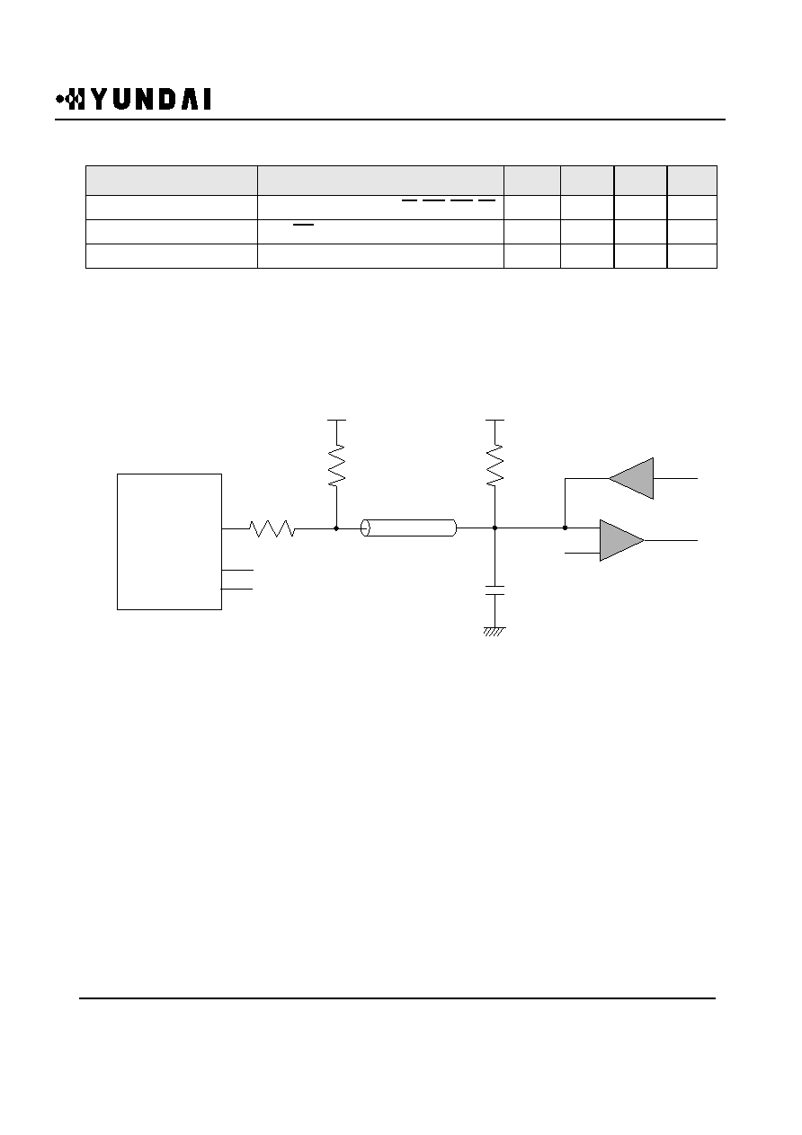
V
R E F
V
T T
V
T T
R
T
=50
R
T
=50
R
S
=25
Zo =50
C
L
= 3 0 p F
D D R S D R A M
D Q
D Q S
V
R E F
V
D D Q
CAPACITANCE
(T
A
=25
o
C, f=1MHz )
Note :
1. VDD, VDDQ = 2.3V to 2.7V, V
ODC
= VDDQ/2, V
O
peak-to-peak = 0.2V
2. Pins not under test are tied to GND.
3. These values are guaranteed by design and are tested on a sample basis only.
OUTPUT LOAD CIRCUIT
Parameter
Pin
Symbol
Min
Max
Unit
Input Capacitance
A0 ~ A12, BA0 ~ BA1, CKE, CS, RAS, CAS, WE
C
IN
2.0
3.0
pF
Clock Capacitance
CLK, CLK
C
CLK
2.0
3.0
pF
Data Input / Output Capacitance
DQ0 ~ DQ3, DQS, DM
C
IO
4.0
5.0
pF