1
Direct RDRAM
TM
256/288-Mbit (512Kx16/18x32s) Preliminary
Rev. 0.9 / Dec.2000
Overview
The Rambus Direct RDRAMTM is a general purpose high-
performance memory device suitable for use in a broad
range of applications including computer memory, graphics,
video, and any other application where high bandwidth and
low latency are required.
The 256/288-Mbit Direct Rambus DRAMs (RDRAM)are
extremely high-speed CMOS DRAMs organized as 16M
words by 16 or 18 bits. The use of Rambus Signaling Level
(RSL) technology permits 600MHz to 800MHz transfer
rates while using conventional system and board design
technologies. Direct RDRAM devices are capable of
sustained data transfers at 1.25 ns per two bytes (10ns per
sixteen bytes).
The architecture of the Direct RDRAMs allows the highest
sustained bandwidth for multiple, simultaneous randomly
addressed memory transactions. The separate control and
data buses with independent row and column control yield
over 95% bus efficiency. The Direct RDRAM's 32 banks
support up to four simultaneous transactions.
System oriented features for mobile, graphics and large
memory systems include power management, byte masking,
and x18 organization. The two data bits in the x18 organiza-
tion are general and can be used for additional storage and
bandwidth or for error correction.
Features
0
Highest sustained bandwidth per DRAM device
- 1.6GB/s sustained data transfer rate
- Separate control and data buses for maximized
efficiency
- Separate row and column control buses for
easy scheduling and highest performance
- 32 banks: four transactions can take place simul-
taneously at full bandwidth data rates
0
Low latency features
- Write buffer to reduce read latency
- 3 precharge mechanisms for controller flexibility
- Interleaved transactions
0
Advanced power management:
- Multiple low power states allows flexibility in power
consumption versus time to transition to active state
- Power-down self-refresh
0
Organization: 2Kbyte pages and 32 banks, x 16/18
- x18 organization allows ECC configurations or
increased storage/bandwidth
- x16 organization for low cost applications
0
Uses Rambus Signaling Level (RSL) for up to 800MHz
operation
The 256/288-Mbit Direct RDRAMs are offered in a uBGA
package suitable for desktop as well as low-profile add-in
card and mobile applications.
Direct RDRAMs operate from a 2.5 volt supply.
Key Timing Parameters / Part Numbers
Figure 1: Direct RDRAM uBGA Package
Organization
a
a. The bank "32s" designation indicates that this RDRAM core is
composed of 32 banks which use a "split" bank architecture.
I/O Freq.
MHz
Core Access Time
(ns)
Part
Number
512
Kx16x32s
600
53
HY5R
256
HC653
512
Kx16x32s
711
45
HY5R
256
HC745
512
Kx16x32s
800
45
HY5R
256
HC845
512
Kx16x32s
800
40
HY5R
256
HC840
512
Kx18x32s
600
53
HY5R
288
HC653
512
Kx18x32s
711
45
HY5R
288
HC745
512
Kx18x32s
800
45
HY5R
288
HC845
512
Kx18x32s
800
40
HY5R
288
HC840
This document is a general product description and is subject to change without notice. Hynix Semiconductor Inc. does not assume any responsibility for use of
circuits described. No patent licenses are implied.
2
Rev.0.9/Dec.2000
Direct RDRAM
TM
256/288-Mbit (512Kx16/18x32s) Preliminary
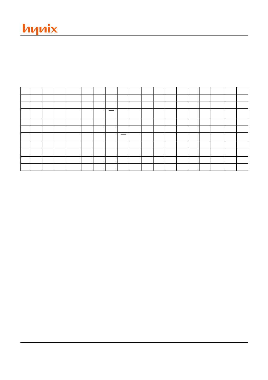
Pinouts and Definitions
Center-Bonded Devices
These tables shows the pin assignments of the center-bonded
RDRAM package from the top-side of the package (the view
looking down on the package as it is mounted on the circuit
board). The mechanical dimensions of this package are
shown in a later section. Refer to Section "" on page 60. (
Note : pin#1 is at the A1 position. )
Table 1: Center-Bonded Device (top view)
10
VDD GND VDD GND VDD VDD VDD VDD GND VDD
9
8
GND VDD CMD VDD GND GNDa GNDa VDD VDD GND GND VDD VDD GND GND VCMOS VDD GND
7
VDD DQA8 DQA7 DQA5 DQA3 DQA1 CTM
CTM ROW
2
ROW
0
COL3 COL1 DQB1 DQB3 DQB5 DQB7 DQB8 VDD
6
5
4
GND GND DQA6 DQA4 DQA2 DQA0 CFM CFM
ROW
1
COL4 COL2 COL0 DQB0 DQB2 DQB4 DQB6 GND GND
3
VDD GND SCK VCMOS GND VDD GND VDDa VREF GND VDD GND GND VDD SIO0 SIO1 GND VDD
2
1
VDD GND GND VDD GND GND GND GND GND VDD
A B C D E F G H J K L M N P R S T U
Rev.0.9 / Dec.2000
3
Direct RDRAM
TM
256/288-Mbit (512Kx16/18x32s) Preliminary
Table 2: Pin Description
Signal
I/O
Type
# Pins
center
Description
SIO1,SIO0
I/O
CMOS
a
2
Serial input/output. Pins for reading from and writing to the control
registers using a serial access protocol. Also used for power manage-
ment.
CMD
I
CMOS
a
1
Command input. Pins used in conjunction with SIO0 and SIO1 for
reading from and writing to the control registers. Also used for power
management.
SCK
I
CMOS
a
1
Serial clock input. Clock source used for reading from and writing to
the control registers
V
DD
24
Supply voltage for the RDRAM core and interface logic.
V
DDa
1
Supply voltage for the RDRAM analog circuitry.
V
CMOS
2
Supply voltage for CMOS input/output pins.
GND
28
Ground reference for RDRAM core and interface.
GNDa
2
Ground reference for RDRAM analog circuitry.
DQA8..DQA0
I/O
RSL
b
9
Data byte A. Nine pins which carry a byte of read or write data
between the Channel and the RDRAM. DQA8 is not used by
RDRAMs with a x16 organization.
CFM
I
RSL
b
1
Clock from master. Interface clock used for receiving RSL signals
from the Channel. Positive polarity.
CFMN
I
RSL
b
1
Clock from master. Interface clock used for receiving RSL signals
from the Channel. Negative polarity
V
REF
1
Logic threshold reference voltage for RSL signals
CTMN
I
RSL
b
1
Clock to master. Interface clock used for transmitting RSL signals to
the Channel. Negative polarity.
CTM
I
RSL
b
1
Clock to master. Interface clock used for transmitting RSL signals to
the Channel. Positive polarity.
RQ7..RQ5 or
ROW2..ROW0
I
RSL
b
3
Row access control. Three pins containing control and address infor-
mation for row accesses.
RQ4..RQ0 or
COL4..COL0
I
RSL
b
5
Column access control. Five pins containing control and address
information for column accesses.
DQB8..
DQB0
I/O
RSL
b
9
Data byte B. Nine pins which carry a byte of read or write data
between the Channel and the RDRAM. DQB8 is not used by
RDRAMs with a x16 organization.
Total pin count per package
92
a. All CMOS signals are high-true; a high voltage is a logic one and a low voltage is logic zero.
b. All RSL signals are low-true; a low voltage is a logic one and a high voltage is logic zero.

4
Rev.0.9/Dec.2000
Direct RDRAM
TM
256/288-Mbit (512Kx16/18x32s) Preliminary
Figure 2: 256/288 Mbit Direct RDRAM Block Diagram
Bank 31
DQA8..DQA0
1
:
8
D
e
m
u
x
8
:
1
M
u
x
W
r
i
t
e
B
u
f
f
e
r
1
:
8
D
e
m
u
x
W
r
i
t
e
B
u
f
f
e
r
8
:
1
M
u
x
Bank 30
Bank 29
Bank 18
Bank 17
Bank 16
Bank 15
Bank 14
Bank 13
Bank 1
Bank 0
S
A
m
p
1
/
2
DQB8..DQB0
9
1:8 Demux
1:8 Demux
Packet Decode
9
5
3
ROW2..ROW0 COL4..COL0
CTM CTMN CFM CFMN
2
SCK,CMD
RCLK
TCLK
Control Registers
DC
COP C
BC MA
MB
DX
XOP BX
DR R
ROP BR
8
8
7
5
5
5
5
5
6
9
5
5
11
AV M S
Write
Buffer
Match
Match
Mux
Match
DEVID
512x128x144
Internal DQB Data Path
Column Decode & Mask
72
9
9
72
9
DM
REFR
Row Decode
Mux
ACT
RD, WR
Power Modes
DRAM Core
Mux
XOP Decode
PREX
PREC
9
9
9
9
72
9
9
9
PRER
COLX
COLC
COLM
2
SIO0,SIO1
Sense Amp
Internal DQA Data Path
Packet Decode
ROWA
ROWR
RCLK
RCLK
R
C
L
K
T
C
L
K
R
C
L
K
T
C
L
K
RQ7..RQ5 or
RQ4..RQ0 or
S
A
m
p
0
/
1
S
A
m
p
0
S
A
m
p
1
4
/
1
5
S
A
m
p
1
5
S
A
m
p
1
3
/
1
4
S
A
m
p
1
6
/
1
7
S
A
m
p
1
7
/
1
8
S
A
m
p
1
6
S
A
m
p
2
9
/
3
0
S
A
m
p
3
0
/
3
1
S
A
m
p
3
1
64x72
S
A
m
p
1
/
2
72
S
A
m
p
0
/
1
S
A
m
p
0
S
A
m
p
1
4
/
1
5
S
A
m
p
1
5
S
A
m
p
1
3
/
1
4
S
A
m
p
1
6
/
1
7
S
A
m
p
1
7
/
1
8
S
A
m
p
1
6
S
A
m
p
2
9
/
3
0
S
A
m
p
3
0
/
3
1
S
A
m
p
3
1
64x72
64x72
Bank 2
�
�
�
�
�
�
�
�
�
�
�
�
�
�
�
�
�
�

5
Direct RDRAM
TM
256/288-Mbit (512Kx16/18x32s) Preliminary
Rev. 0.9 / Dec.2000
General Description
Figure 2: is a block diagram of the 256/288 Mbit Direct
RDRAM. It consists of two major blocks: a "core" block
built from banks and sense amps similar to those found in
other types of DRAM, and a Direct Rambus interface block
which permits an external controller to access this core at up
to 1.6GB/s.
Control Registers:
The CMD, SCK, SIO0, and SIO1
pins appear in the upper center of Figure 2:. They are used to
write and read a block of control registers. These registers
supply the RDRAM configuration information to a
controller and they select the operating modes of the device.
The REFR value is used for tracking the last refreshed row.
Most importantly, the five bit DEVID specifies the device
address of the RDRAM on the Channel.
Clocking:
The CTM and CTMN pins (Clock-To-Master)
generate TCLK (Transmit Clock), the internal clock used to
transmit read data. The CFM and CFMN pins (Clock-From-
Master) generate RCLK (Receive Clock), the internal clock
signal used to receive write data and to receive the ROW and
COL pins.
DQA,DQB Pins:
These 18 pins carry read (Q) and write
(D) data across the Channel. They are multiplexed/de-multi-
plexed from/to two 72-bit data paths (running at one-eighth
the data frequency) inside the RDRAM.
Banks:
The 32Mbyte core of the RDRAM is divided into
32 x 1Mbyte banks, each organized as 512 rows, with each
row containing 128 dualocts(2K bytes), and each dualoct
containing 16 bytes. A dualoct is the smallest unit of data
that can be addressed.
Sense Amps:
The RDRAM contains
34 sense amps.
Each sense amp consists of 1K bytes of fast storage (512
bytes for DQA and 512 bytes for DQB) and can hold one-
half of one row of one bank of the RDRAM. The sense amp
may hold any of the 1024 half-rows of an associated bank.
However, each sense amp is shared between two adjacent
banks of the RDRAM (except for sense amps 0, 15, 16, and
31). This introduces the restriction that adjacent banks may
not be simultaneously accessed.
RQ Pins:
These pins carry control and address informa-
tion. They are broken into two groups. RQ7..RQ5 are also
called ROW2..ROW0, and are used primarily for controlling
row accesses. RQ4..RQ0 are also called COL4..COL0, and
are used primarily for controlling column accesses.
ROW Pins:
The principle use of these three pins is to
manage the transfer of data between the banks and the sense
amps of the RDRAM. These pins are de-multiplexed into a
24-bit ROWA (row-activate) or ROWR (row-operation)
packet.
COL Pins:
The principle use of these five pins is to
manage the transfer of data between the DQA/DQB pins and
the sense amps of the RDRAM. These pins are de-multi-
plexed into a 23-bit COLC (column-operation) packet and
either a 17-bit COLM (mask) packet or a 17-bit COLX
(extended-operation) packet.
ACT Command:
An ACT (activate) command from an
ROWA packet causes one of the 512 rows of the selected
bank to be loaded to its associated sense amps (two 512
bytes sense amps for DQA and two for DQB).
PRER Command:
A PRER (precharge) command from
an ROWR packet causes the selected bank to release its two
associated sense amps, permitting a different row in that
bank to be activated, or permitting adjacent banks to be acti-
vated.
RD Command:
The RD (read) command causes one of
the 64 dualocts of one of the sense amps to be transmitted on
the DQA/DQB pins of the Channel.
WR Command:
The WR (write) command causes a
dualoct received from the DQA/DQB data pins of the
Channel to be loaded into the write buffer. There is also
space in the write buffer for the BC bank address and C
column address information. The data in the write buffer is
automatically retired (written with optional bytemask) to one
of the 128 dualocts of one of the sense amps during a subse-
quent COP command. A retire can take place during a RD,
WR, or NOCOP to another device, or during a WR or
NOCOP to the same device. The write buffer will not retire
during a RD to the same device. The write buffer reduces the
delay needed for the internal DQA/DQB data path turn-
around.
PREC Precharge:
The PREC, RDA and WRA
commands are similar to NOCOP, RD and WR, except that a
precharge operation is performed at the end of the column
operation. These commands provide a second mechanism
for performing precharge.
PREX Precharge:
After a RD command, or after a WR
command with no byte masking (M=0), a COLX packet may
be used to specify an extended operation (XOP). The most
important XOP command is PREX. This command provides
a third mechanism for performing precharge.