HY5V56B(L/S)F Series
4 Banks x 4M x 16bits Synchronous DRAM
This document is a general product description and is subject to change without notice. Hynix does not assume any responsibility for
use of circuits described. No patent licenses are implied.
Rev. 0.1/Oct. 02 2
DESCRIPTION
Preliminary
The HY5V56B(L)F is a 268,435,456bit CMOS Synchronous DRAM, ideally suited for the Mobile applications which
require low power consumption and industrial temperature range. HY5V56B(L)F is organized as 4banks of
4,194,304x16
HY5V56B(L)F is offering fully synchronous operation referenced to a positive edge of the clock. All inputs and outputs
are synchronized with the rising edge of the clock input. The data paths are internally pipelined to achieve very high
bandwidth. All input and output voltage levels are compatible with LVTTL.
Programmable options include the length of pipeline (Read latency of 2 or 3), the number of consecutive read or write
cycles initiated by a single control command (Burst length of 1,2,4,8, or full page), and the burst count
sequence(sequential or interleave). A burst of read or write cycles in progress can be terminated by a burst terminate
command or can be interrupted and replaced by a new burst read or write command on any cycle. (This pipelined
design is not restricted by a `2N` rule.)
FEATURES
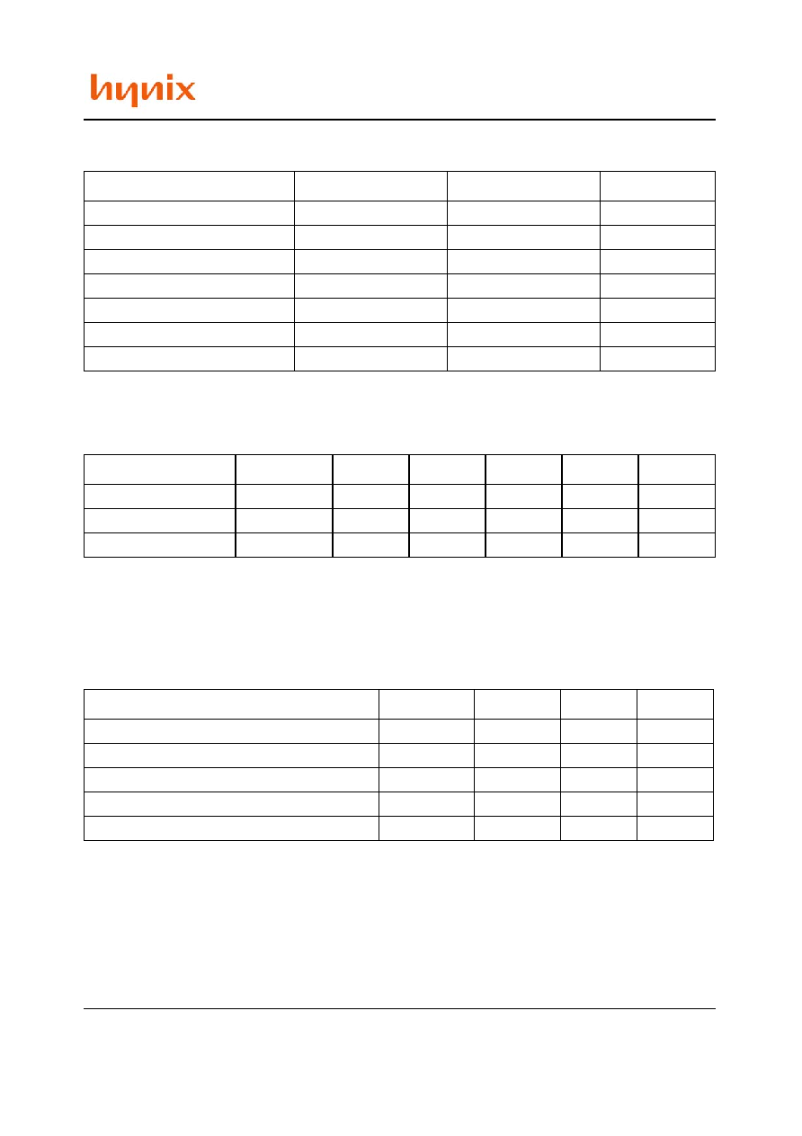
ORDERING INFORMATION
Part No.
Clock Frequency
Power
Organization
Interface
Package
HY5V56BF-H
133MHz
Normal
4Banks x 4Mbits
x16
LVTTL
54ball FBGA
HY5V56BF-8
125MHz
HY5V56BF-P
100MHz
HY5V56BF-S
100MHz
HY5V56B(L)F-H
133MHz
Low power
HY5V56B(L)F-8
125MHz
HY5V56B(L)F-P
100MHz
HY5V56B(L)F-S
100MHz
�
Single 3.3�0.3V power supply
�
All device balls are compatible with LVTTL interface
�
54Ball FBGA (13.5mm x 8.0mm)
�
All inputs and outputs referenced to positive edge of
system clock
�
Data mask function by UDQM or LDQM
�
Internal four banks operation
�
Auto refresh and self refresh
�
8192 refresh cycles / 64ms
�
Programmable Burst Length and Burst Type
- 1, 2, 4, 8 or Full page for Sequential Burst
- 1, 2, 4 or 8 for Interleave Burst
�
Programmable CAS Latency ; 2, 3 Clocks
HY5V56B(L/S)F
Rev. 0.1/Oct. 02 3
BALL CONFIGURATION
A
B
C
D
E
F
G
H
J
54 Ball
FBGA
0.8 mm
Ball Pitch
VSS
DQ15
VSSQ
DQ14
DQ13
VDDQ
DQ12
DQ11
VSSQ
DQ10
DQ9
VDDQ
DQ8
CLK
VSS
UDQM
A11
CKE
A12
A9
A8
A7
A6
VSS
A5
A4
NC
1
2
3
A
B
C
D
E
F
G
H
J
VDDQ
VDDQ
VSSQ
VSSQ
VDD
DQ0
VDD
VDD
DQ2
DQ1
DQ4
DQ3
DQ6
DQ5
DQ7
LDQM
/CAS
/RAS
/WE
A3
A2
A0
A1
A10
/CS
BA0
BA1
7
8
9
9
8
7
3
2
1
< Top View >
< Bottom View >
HY5V56B(L/S)F
BALL DESCRIPTION
BALL OUT
SYMBOL
TYPE
DESCRIPTION
F2
CLK
INPUT
Clock : The system clock input. All other inputs are registered
to the SDRAM on the rising edge of CLK
F3
CKE
INPUT
Clock Enable : Controls internal clock signal and when deacti-
vated, the SDRAM will be one of the states among power
down, suspend or self refresh
G9
CS
INPUT
Chip Select : Enables or disables all inputs except CLK, CKE,
UDQM and LDQM
G7,G8
BA0, BA1
INPUT
Bank Address : Selects bank to be activated during RAS activ-
ity
Selects bank to be read/written during CAS activity
H7, H8, J8, J7,
J3, J2, H3, H2,
H1, G3, H9, G2,
G1
A0 ~ A12
INPUT
Row Address : RA0 ~ RA12, Column Address : CA0 ~ CA8
Auto-precharge flag : A10
F8, F7, F9
RAS, CAS,
WE
INPUT
Command Inputs : RAS, CAS and WE define the operation
Refer function truth table for details
F1, E8
UDQM,
LDQM
INPUT
Data Mask:Controls output buffers in read mode and masks
input data in write mode
A8, B9, B8, C9,
C8, D9, D8, E9,
E1, D2, D1, C2,
C1, B2, B1, A2
DQ0 ~
DQ15
I/O
Data Input/Output:Multiplexed data input/output ball
A9, E7, J9, A1,
E3, J1
VDD/VSS
SUPPLY
Power supply for internal circuits
A7, B3, C7, D3,
A3, B7, C3, D7
VDDQ/
VSSQ
SUPPLY
Power supply for output buffers
E2, G1
NC
-
No connection
HY5V56B(L/S)F
Rev. 0.1/Oct. 02 5
FUNCTIONAL BLOCK DIAGRAM
4Mbit x 4banks x 16 I/O Synchronous DRAM
X
de
code
r
s
St
at
e M
a
ch
i
n
e
A0
A1
A11
BA0
BA1
Addr
ess b
u
ff
e
r
s
Address
Registers
Mode Registers
Row
Pre
Decoders
Column
Pre
Decoders
Column Add
Counter
Row active
Column
Active
Burst
Counter
Data Out Control
CAS Latency
Internal Row
counter
DQ0
DQ1
DQ14
DQ15
refresh
Self refresh logic
& timer
Pipe Line Control
I/O Buff
e
r
& L
ogic
Bank Select
Sens
e AM
P &
I/
O Gate
CLK
CKE
CS
RAS
CAS
WE
UDQM
LDQM
4Mx16 Bank 3
X d
e
c
o
d
e
r
s
X d
e
c
o
d
e
r
s
Memory
Cell
Array
Y decoders
X
de
code
r
s
4Mx16 Bank 0
4Mx16 Bank 1
4Mx16 Bank 2
X
de
code
r
s
X
de
code
r
s
St
at
e M
a
ch
i
n
e
A0
A1
A12
BA0
BA1
Addr
ess b
u
ff
e
r
s
Address
Registers
Mode Registers
Row
Pre
Decoders
Column
Pre
Decoders
Column Add
Counter
Row active
Column
Active
Burst
Counter
Data Out Control
CAS Latency
Internal Row
counter
DQ0
DQ1
DQ14
DQ15
refresh
Self refresh logic
& timer
Pipe Line Control
I/O Buff
e
r
& L
ogic
Bank Select
Sens
e AM
P &
I/
O Gate
CLK
CKE
CS
RAS
CAS
WE
UDQM
LDQM
4Mx16 Bank 3
X d
e
c
o
d
e
r
s
X d
e
c
o
d
e
r
s
X d
e
c
o
d
e
r
s
X d
e
c
o
d
e
r
s
Memory
Cell
Array
Y decoders
X
de
code
r
s
Memory
Cell
Array
Y decoders
X
de
code
r
s
4Mx16 Bank 0
4Mx16 Bank 1
4Mx16 Bank 2
X
de
code
r
s
X
de
code
r
s
St
at
e M
a
ch
i
n
e
A0
A1
A11
BA0
BA1
Addr
ess b
u
ff
e
r
s
Address
Registers
Mode Registers
Row
Pre
Decoders
Column
Pre
Decoders
Column Add
Counter
Row active
Column
Active
Burst
Counter
Data Out Control
CAS Latency
Internal Row
counter
DQ0
DQ1
DQ14
DQ15
refresh
Self refresh logic
& timer
Pipe Line Control
I/O Buff
e
r
& L
ogic
Bank Select
Sens
e AM
P &
I/
O Gate
CLK
CKE
CS
RAS
CAS
WE
UDQM
LDQM
4Mx16 Bank 3
X d
e
c
o
d
e
r
s
X d
e
c
o
d
e
r
s
X d
e
c
o
d
e
r
s
X d
e
c
o
d
e
r
s
Memory
Cell
Array
Y decoders
X
de
code
r
s
Memory
Cell
Array
Y decoders
X
de
code
r
s
4Mx16 Bank 0
4Mx16 Bank 1
4Mx16 Bank 2
X
de
code
r
s
X
de
code
r
s
St
at
e M
a
ch
i
n
e
A0
A1
A12
BA0
BA1
Addr
ess b
u
ff
e
r
s
Address
Registers
Mode Registers
Row
Pre
Decoders
Column
Pre
Decoders
Column Add
Counter
Row active
Column
Active
Burst
Counter
Data Out Control
CAS Latency
Internal Row
counter
DQ0
DQ1
DQ14
DQ15
refresh
Self refresh logic
& timer
Pipe Line Control
I/O Buff
e
r
& L
ogic
Bank Select
Sens
e AM
P &
I/
O Gate
CLK
CKE
CS
RAS
CAS
WE
UDQM
LDQM
4Mx16 Bank 3
X d
e
c
o
d
e
r
s
X d
e
c
o
d
e
r
s
X d
e
c
o
d
e
r
s
X d
e
c
o
d
e
r
s
Memory
Cell
Array
Y decoders
X
de
code
r
s
Memory
Cell
Array
Y decoders
X
de
code
r
s
4Mx16 Bank 0
4Mx16 Bank 1
4Mx16 Bank 2
Memory
Cell
Array
Y decoders
X
de
code
r
s
Memory
Cell
Array
Y decoders
X
de
code
r
s
4Mx16 Bank 0
4Mx16 Bank 1
4Mx16 Bank 2
HY5V56B(L/S)F
Rev. 0.1/Oct. 02 6
ABSOLUTE MAXIMUM RATINGS
Note : Operation at above absolute maximum rating can adversely affect device reliability.
DC OPERATING CONDITION
(T
A
= 0
�C to 70�C)
Note :
1.All voltages are referenced to V
SS
= 0V
2.V
IH
(max) is acceptable 5.6V AC pulse width with <=3ns of duration.
3.V
IL
(min) is acceptable -2.0V AC pulse width with <=3ns of duration.
AC OPERATING TEST CONDITION
(T
A
= 0
�C to 70�C, V
DD
=3.3
�
0.3V, V
SS
=0V)
Note :
1.Output load to measure access times is equivalent to two TTL gates and one capacitor (50pF). For details, refer to AC/DC output
load circuit
Parameter
Symbol
Rating
Unit
Ambient Temperature
T
A
0 ~ 70
�C
Storage Temperature
T
STG
-55 ~ 125
�C
Voltage on Any ball relative to V
SS
V
IN
, V
OUT
-1.0 ~ 4.6
V
Voltage on V
DD
relative to V
SS
V
DD,
V
DDQ
-1.0 ~ 4.6
V
Short Circuit Output Current
I
OS
50
mA
Power Dissipation
P
D
1
W
Soldering Temperature
Time
T
SOLDER
260
10
�C Sec
Parameter
Symbol
Min
Typ
Max
Unit
Note
Power Supply Voltage
V
DD
, V
DDQ
3.0
3.3
3.6
V
1
Input High voltage
V
IH
2.0
3.0
V
DDQ
+ 0.3
V
1,2
Input Low voltage
V
IL
-0.3
0
0.8
V
1,3
Parameter
Symbol
Value
Unit
Note
AC Input High / Low Level Voltage
V
IH
/ V
IL
2.4/0.4
V
Input Timing Measurement Reference Level Voltage
Vtrip
1.4
V
Input Rise / Fall Time
tR / tF
1
ns
Output Timing Measurement Reference Level Voltage
Voutref
1.4
V
Output Load Capacitance for Access Time Measurement
C
L
50
pF
1
HY5V56B(L/S)F
Rev. 0.1/Oct. 02 7
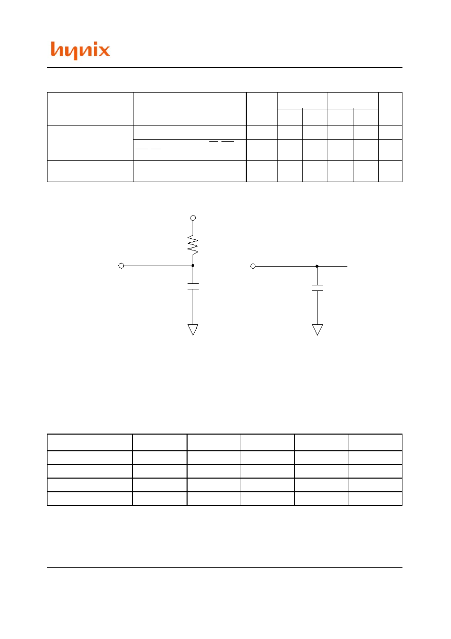
CAPACITANCE
(TA=25
�C, f=1MHz)
OUTPUT LOAD CIRCUIT
DC CHARACTERISTICS I
(TA= 0
�C to 70�C, V
DD
=3.3
�
0.3V)
Note :
1.V
IN
= 0 to 3.6V, All other balls are not tested under V
IN
=0V
2.D
OUT
is disabled, V
OUT
=0 to 3.6
Parameter
ball
Symbol
-H
-8/P/S
Unit
Min
Max
Min
Max
Input capacitance
CLK
C
I1
2.5
3.5
2.5
4.0
pF
A0 ~ A12, BA0, BA1, CKE, CS, RAS,
CAS, WE, UDQM, LDQM
CI
2
2.5
3.8
2.5
5.0
pF
Data input / output capaci-
tance
DQ0 ~ DQ15
C
I/O
4.0
6.5
4.0
6.5
pF
Parameter
Symbol
Min.
Max
Unit
Note
Input Leakage Current
I
LI
-1
1
uA
1
Output Leakage Current
I
LO
-1
1
uA
2
Output High Voltage
V
OH
2.4
-
V
I
OH
= -2mA
Output Low Voltage
V
OL
-
0.4
V
I
OL
= +2mA
Vtt=1.4V
RT=250
50pF
Output
50pF
Output
DC Output Load Circuit
AC Output Load Circuit
HY5V56B(L/S)F
Rev. 0.1/Oct. 02 8
DC CHARACTERISTICS II
(TA= 0
�C to 70�C, V
DD
=3.3
�
0.3V, V
SS
=0V)
Note :
1.I
DD1
and I
DD4
depend on output loading and cycle rates. Specified values are measured with the output open
2.Min. of tRRC (Refresh RAS cycle time) is shown at AC CHARACTERISTICS II
3.HY5V56BF-H/8/P/S
4.HY5V56BLF-H/8/P/S
5.HY5V56BSF-H/8/P/S
Parameter
Symbol
Test Condition
Unit
Note
-H
-8
-P
-S
Operating Current
I
DD1
Burst length=1, One bank active
t
RC
t
RC
(min), I
OL
=0mA
120
120
110
110
mA
1
Precharge Standby Current
in Power Down Mode
I
DD2P
CKE
V
IL
(max), t
CK
= 15ns
2
mA
I
DD2PS
CKE
V
IL
(max), t
CK
=
1
Precharge Standby Current
in Non Power Down Mode
I
DD2N
CKE
V
IH
(min), CS
V
IH
(min), t
CK
= 15ns
Input signals are changed one time during
30ns. All other balls
V
DD
-0.2V or
0.2V
30
mA
I
DD2NS
CKE
V
IH
(min), t
CK
=
Input signals are stable.
15
Active Standby Current
in Power Down Mode
I
DD3P
CKE
V
IL
(max), t
CK
= 15ns
5
mA
I
DD3PS
CKE
V
IL
(max), t
CK
=
5
Active Standby Current
in Non Power Down Mode
I
DD3N
CKE
V
IH
(min), CS
V
IH
(min), t
CK
= 15ns
Input signals are changed one time during
30ns. All other balls
V
DD
-0.2V or
0.2V
40
mA
I
DD3NS
CKE
V
IH
(min), t
CK
=
Input signals are stable.
30
Burst Mode Operating
Current
I
DD4
t
CK
t
CK
(min), I
OL
=0mA
All banks active
CL=3
130
130
110
110
mA
1
CL=2
140
140
120
120
Auto Refresh Current
I
DD5
t
RRC
t
RRC
(min), All banks active
220
200
200
200
mA
2
Self Refresh Current
I
DD6
CKE
0.2V
Normal
3
mA
3
Low Power
1.5
mA
4
SL Power
800
uA
5
HY5V56B(L/S)F
Rev. 0.1/Oct. 02 9
AC CHARACTERISTICS I
(AC operating conditions unless otherwise noted)
Note :
1.Assume tR / tF (input rise and fall time ) is 1ns
If tR & tF > 1ns, then [(tR+tF)/2-1]ns should be added to the parameter
2.Access times to be measured with input signals of 1v/ns edge rate, from 0.8v to 2.0v
If tR > 1ns, then (tR/2-0.5)ns should be added to the parameter
Parameter
Symbol
-H
-8
-P
-S
Unit
Note
Min
Max
Min
Max
Min
Max
Min
Max
System Clock Cycle
Time
CAS Latency = 3
tCK3
7.5
1000
8
1000
10
1000
10
1000
ns
CAS Latency = 2
tCK2
10
10
10
12
ns
Clock High Pulse Width
tCHW
2.5
-
3
-
3
-
3
-
ns
1
Clock Low Pulse Width
tCLW
2.5
-
3
-
3
-
3
-
ns
1
Access Time From
Clock
CAS Latency = 3
tAC3
-
5.4
-
6
-
6
-
6
ns
2
CAS Latency = 2
tAC2
-
6
-
6
-
6
-
6
ns
Data-Out Hold Time
tOH
2.5
-
2.5
-
2.5
-
2.5
-
ns
Data-Input Setup Time
tDS
2
-
2
-
2
-
2
-
ns
1
Data-Input Hold Time
tDH
0.8
-
1
-
1
-
1
-
ns
1
Address Setup Time
tAS
1.5
-
2
-
2
-
2
-
ns
1
Address Hold Time
tAH
0.8
-
1
-
1
-
1
-
ns
1
CKE Setup Time
tCKS
1.5
-
2
-
2
-
2
-
ns
1
CKE Hold Time
tCKH
0.8
-
1
-
1
-
1
-
ns
1
Command Setup Time
tCS
1.5
-
2
-
2
-
2
-
ns
1
Command Hold Time
tCH
0.8
-
1
-
1
-
1
-
ns
1
CLK to Data Output in Low-Z Time
tOLZ
1
-
1
-
1
-
1
-
ns
CLK to Data Output in
High-Z Time
CAS Latency = 3
tOHZ3
2.0
5.4
2.0
6
2.0
6
2.0
6
ns
CAS Latency = 2
tOHZ2
2.0
6
2.0
6
2.0
6
2.0
6
ns
HY5V56B(L/S)F
Rev. 0.1/Oct. 02 10
AC CHARACTERISTICS II
Note :
1. A new command can be given tRRC after self refresh exit
Parameter
Symbol
-H
-8
-P
-S
Unit
Note
Min
Max
Min
Max
Min
Max
Min
Max
RAS Cycle Time
Operation
tRC
65
-
68
-
70
-
70
-
ns
Auto Refresh
tRRC
65
-
68
-
70
-
70
-
ns
RAS to CAS Delay
tRCD
20
-
20
-
20
-
20
-
ns
RAS Active Time
tRAS
45
100K
48
100K
50
100K
50
100K
ns
RAS Precharge Time
tRP
20
-
20
-
20
-
20
-
ns
RAS to RAS Bank Active Delay
tRRD
15
-
16
-
20
-
20
-
ns
CAS to CAS Delay
tCCD
1
-
1
-
1
-
1
-
CLK
Write Command to Data-In Delay
tWTL
0
-
0
-
0
-
0
-
CLK
Data-In to Precharge Command
tDPL
2
-
2
-
2
-
2
-
CLK
Data-In to Active Command
tDAL
5
-
5
-
5
-
5
-
CLK
DQM to Data-Out Hi-Z
tDQZ
2
-
2
-
2
-
2
-
CLK
DQM to Data-In Mask
tDQM
0
-
0
-
0
-
0
-
CLK
MRS to New Command
tMRD
2
-
2
-
2
-
2
-
CLK
Precharge to Data
Output Hi-Z
CAS Latency = 3
tPROZ3
3
-
3
-
3
-
3
-
CLK
CAS Latency = 2
tPROZ2
2
-
2
-
2
-
2
-
CLK
Power Down Exit Time
tPDE
1
-
1
-
1
-
1
-
CLK
Self Refresh Exit Time
tSRE
1
-
1
-
1
-
1
-
CLK
1
Refresh Time
tREF
-
64
-
64
-
64
-
64
ms
HY5V56B(L/S)F
Rev. 0.1/Oct. 02 11
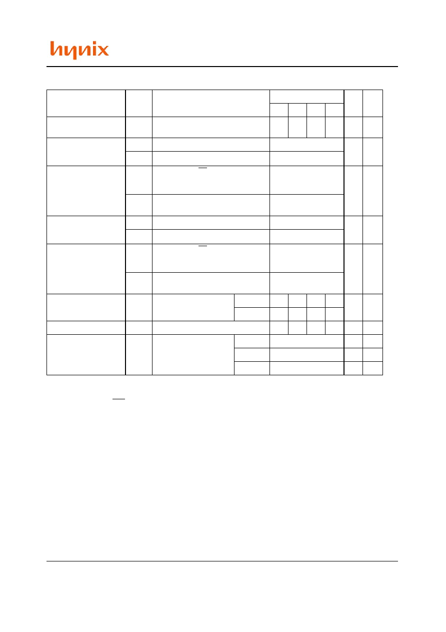
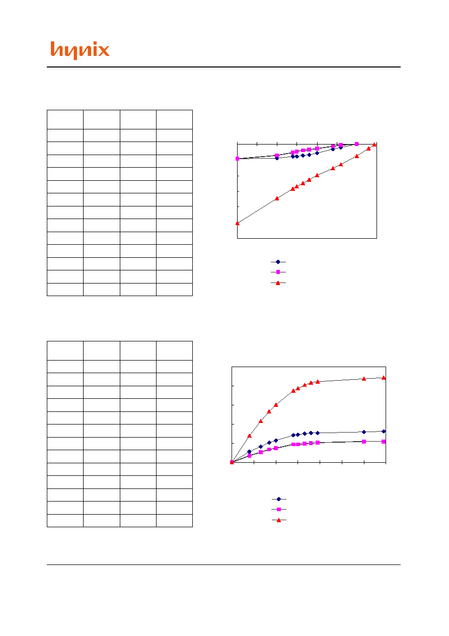
IBIS SPECIFICATION
I
OH
Characteristics (Pull-up)
I
OL
Characteristics (Pull-down)
Voltage
100MHz
(Min)
100MHz
(Max)
66MHz
(Min)
(V)
I(mA)
I(mA)
I(mA)
3.45
-2.4
3.3
-27.3
3.0
0
-74.1
-0.7
2.6
-21.1
-129.2
-7.5
2.4
-34.1
-153.3
-13.3
2.0
-58.7
-197
-27.5
1.8
-67.3
-226.2
-35.5
1.65
-73
-248
-41.1
1.5
-77.9
-269.7
-47.9
1.4
-80.8
-284.3
-52.4
1.0
-88.6
-344.5
-72.5
0
-93
-502.4
-93
Voltage
100MHz
(Min)
100MHz
(Max)
66MHz
(Min)
(V)
I(mA)
I(mA)
I(mA)
0
0
0
0
0.4
27.5
70.2
17.7
0.65
41.8
107.5
26.9
0.85
51.6
133.8
33.3
1.0
58.0
151.2
37.6
1.4
70.7
187.7
46.6
1.5
72.9
194.4
48.0
1.65
75.4
202.5
49.5
1.8
77.0
208.6
50.7
1.95
77.6
212.0
51.5
3.0
80.3
219.6
54.2
3.45
81.4
222.6
54.9
-600
-500
-400
-300
-200
-100
0
0
0.5
1
1.5
2
2.5
3
3.5
Voltage (V)
I (mA)
I
OH
Min (66MHz)
I
OH
Min (100MHz)
I
OH
Max (66 /100MHz)
66MHz and 100MHz Pull-up
0
50
100
150
200
250
0
0.5
1
1.5
2
2.5
3
3.5
Voltage (V)
I (mA)
66MHz and 100MHz Pull-down
I
OL
Min (100MHz)
I
OL
Min (66MHz)
I
OL
Max (100MHz)
HY5V56B(L/S)F
Rev. 0.1/Oct. 02 12
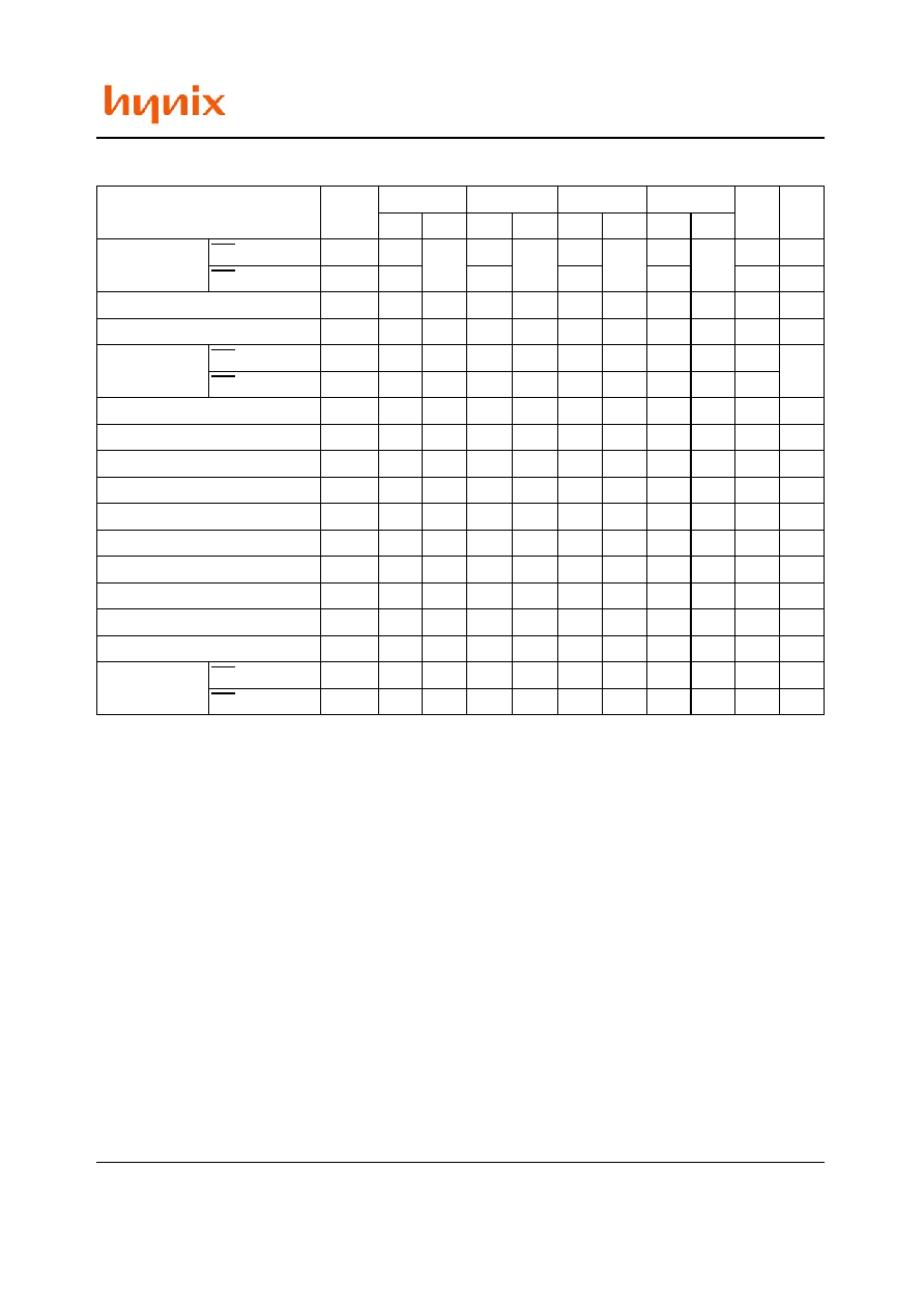
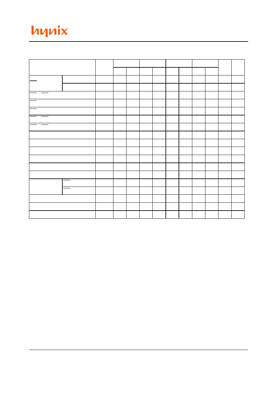
DEVICE OPERATING OPTION TABLE
HY5V56B(L)F-H
HY5V56B(L)F-8
HY5V56B(L)F-P
HY5V56B(L)F-S
CAS Latency
tRCD
tRAS
tRC
tRP
tAC
tOH
133MHz(7.5ns)
3CLKs
3CLKs
6CLKs
9CLKs
3CLKs
5.4ns
2.0ns
125MHz(8ns)
3CLKs
3CLKs
6CLKs
9CLKs
3CLKs
6ns
2.0ns
100MHz(10ns)
2CLKs
2CLKs
5CLKs
7CLKs
2CLKs
6ns
2.0ns
CAS Latency
tRCD
tRAS
tRC
tRP
tAC
tOH
125MHz(8ns)
3CLKs
3CLKs
6CLKs
9CLKs
3CLKs
6ns
2.0ns
100MHz(10ns)
2CLKs
2CLKs
5CLKs
7CLKs
2CLKs
6ns
2.0ns
83MHz(12ns)
2CLKs
2CLKs
4CLKs
6CLKs
2CLKs
6ns
2.0ns
CAS Latency
tRCD
tRAS
tRC
tRP
tAC
tOH
100MHz(10ns)
2CLKs
2CLKs
5CLKs
7CLKs
2CLKs
6ns
2.0ns
83MHz(12ns)
2CLKs
2CLKs
5CLKs
7CLKs
2CLKs
6ns
2.0ns
66MHz(15ns)
2CLKs
2CLKs
4CLKs
6CLKs
2CLKs
6ns
2.0ns
CAS Latency
tRCD
tRAS
tRC
tRP
tAC
tOH
100MHz(10ns)
3CLKs
2CLKs
5CLKs
7CLKs
2CLKs
6ns
2.0ns
83MHz(12ns)
2CLKs
2CLKs
5CLKs
7CLKs
2CLKs
6ns
2.0ns
66MHz(15ns)
2CLKs
2CLKs
4CLKs
6CLKs
2CLKs
6ns
2.0ns
HY5V56B(L/S)F
Rev. 0.1/Oct. 02 13
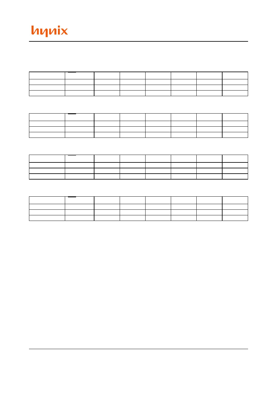
COMMAND TRUTH TABLE
Note :
1. Exiting Self Refresh occurs by asynchronously bringing CKE from low to high
2. X = Don
t care, H = Logic High, L = Logic Low. BA =Bank Address, RA = Row Address, CA = Column Address,
Opcode = Operand Code, NOP = No Operation
3. The burst read sigle write mode is entered by programming the write burst mode bit (A9) in the mode register to a logic 1.
Command
CKEn-1
CKEn
CS
RAS
CAS
WE
DQM
ADDR
A10/
AP
BA
Note
Mode Register Set
H
X
L
L
L
L
X
OP code
No Operation
H
X
H
X
X
X
X
X
L
H
H
H
Bank Active
H
X
L
L
H
H
X
RA
V
Read
H
X
L
H
L
H
X
CA
L
V
Read with Autoprecharge
H
Write
H
X
L
H
L
L
X
CA
L
V
Write with Autoprecharge
H
Precharge All Banks
H
X
L
L
H
L
X
X
H
X
Precharge selected Bank
L
V
Burst Stop
H
X
L
H
H
L
X
X
DQM
H
X
V
X
Auto Refresh
H
H
L
L
L
H
X
X
Burst-Read-Single-
WRITE
H
X
L
L
L
L
X
A9 ball High
(Other balls OP code)
MRS
Mode
Self Refresh
1
Entry
H
L
L
L
L
H
X
X
Exit
L
H
H
X
X
X
X
L
H
H
H
Precharge
power down
Entry
H
L
H
X
X
X
X
X
L
H
H
H
Exit
L
H
H
X
X
X
X
L
H
H
H
Clock
Suspend
Entry
H
L
H
X
X
X
X
X
L
V
V
V
Exit
L
H
X
X
HY5V56B(L/S)F
Rev. 0.1/Oct. 02 14
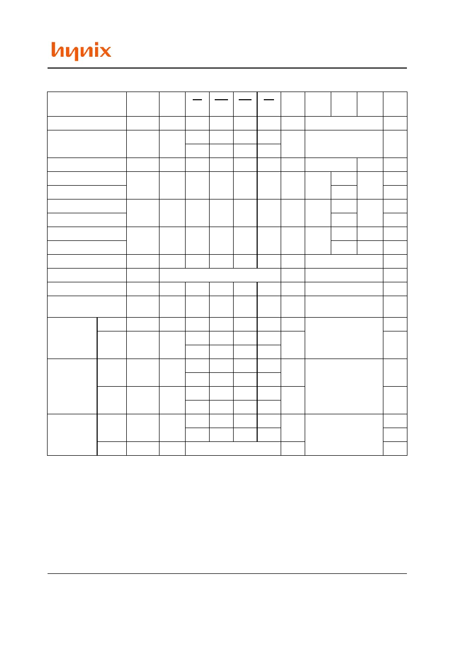
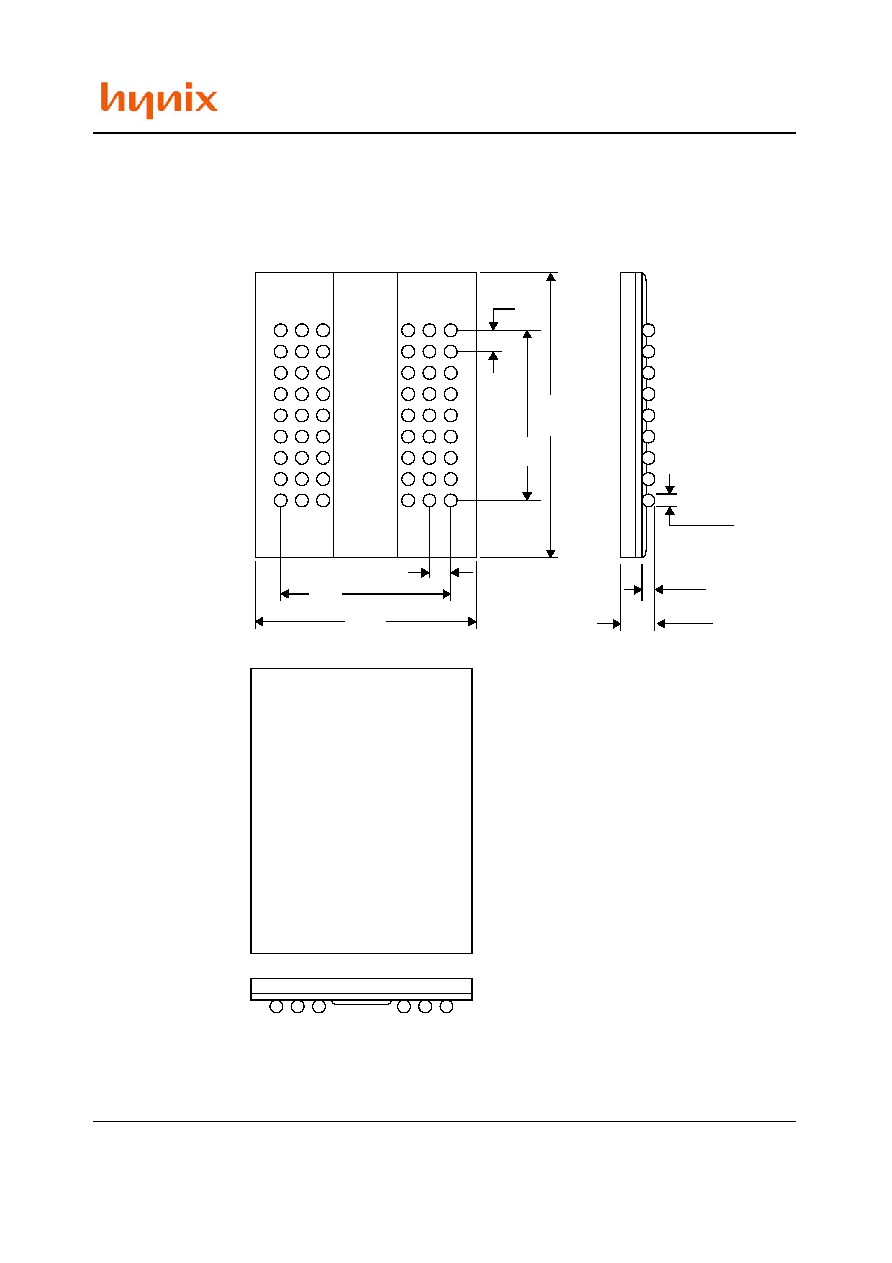
PACKAGE INFORMATION
54 Ball 0.8mm pitch 8.0mm x 13.5mm FBGA
13.50
6.40
0.80
8.00
0.80
6.40
1.070
0.340
0.450