Preliminary
HY5W5A6DF-xF
4Banks x 4M x 16bits Synchronous DRAM
This document is a general product description and is subject to change without notice. Hynix does not assume any responsibility for
use of circuits described. No patent licenses are implied.
Rev. 0.4 / June. 2003
DESCRIPTION
The Hynix Low Power SDRAM is suited for non-PC application which use the batteries such as PDAs,
2.5G and 3G cellular phones with internet access and multimedia capabilities, mini-notebook, handheld
PCs.
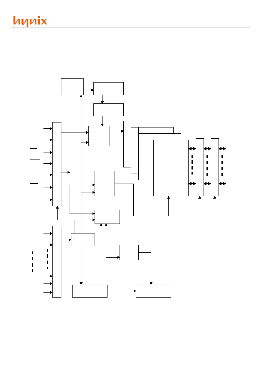
The Hynix HY5W5A6DF is a 268,435,456bit CMOS Synchronous Dynamic Random Access Memory. It
is organized as 4banks of 4,194,304x16.
The Low Power SDRAM provides for programmable options including CAS latency of 1, 2, or 3, READ
or WRITE burst length of 1, 2, 4, 8, or full page, and the burst count sequence(sequential or interleave).
And the Low Power SDRAM also provides for special programmable options including Partial Array Self
Refresh of a quarter bank, a half bank, 1bank, 2banks, or all banks, Temperature Compensated Self
Refresh of 15, 45, 70, or 85 degrees C. A burst of Read or Write cycles in progress can be terminated
by a burst terminate command or can be interrupted and replaced by a new burst Read or Write com-
mand on any cycle(This pipelined design is not restricted by a 2N rule).
Deep Power Down Mode is a additional operating mode for Low Power SDRAM. This mode can achieve
maximum power reduction by removing power to the memory array within each SDRAM. By using this
feature, the system can cut off alomost all DRAM power without adding the cost of a power switch and
giving up mother-board power-line layout flexibility.
FEATURES
∑ Standard SDRAM Protocol
∑ Internal 4bank operation
∑ Voltage : VDD = 2.5V, VDDQ = 1.8V & 2.5V
∑ LVCMOS compatible I/O Interface
∑ Low Voltage interface to reduce I/O power
∑ Low Power Features ( HY5W56DF Series can't support these features)
- PASR(Partial Array Self Refresh)
- TCSR(Temperature Compensated Self Refresh)
- DS(Drive Strength)
- Deep Power Down Mode
∑ CAS latency of 1, 2, or 3
∑ Packages : 54ball, 0.8mm pitch FBGA
∑ -25 ~ 70C Operation
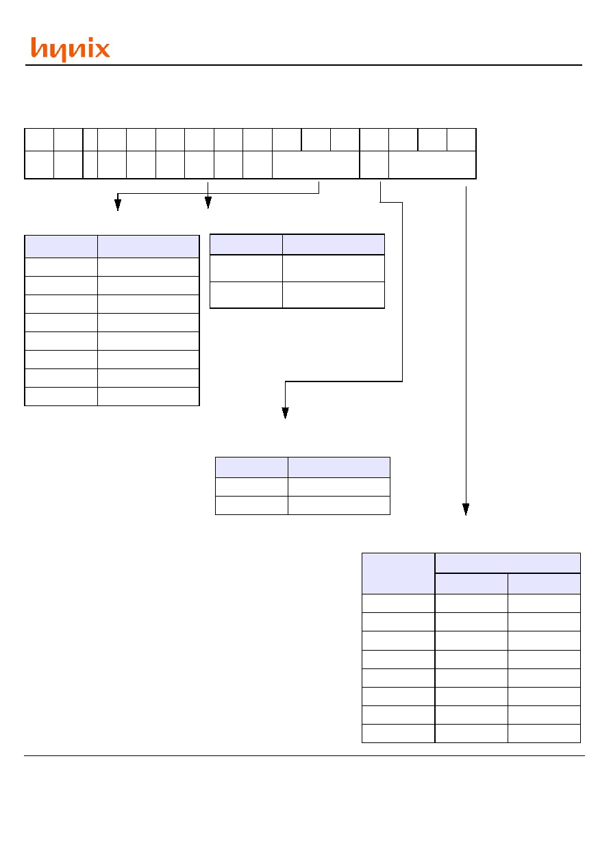
ORDERING INFORMATION
Part Number
Clock
Frequency
CAS
Latency
Organization
Interface
Package
HY5W5A6D(L/S)F-HF
HY5W56DF-HF
133MHz
3
4banks x 4Mb x 16
LVCMOS
54ball
FBGA
HY5W5A6D(L/S)F-PF
HY5W56DF-PF
105MHz
2
4banks x 4Mb x 16
LVCMOS
HY5W5A6D(L/S)F-SF
HY5W66DF-SF
105MHz
3
4banks x 4Mb x 16
LVCMOS
HHY5W5A6D(L/S)F-BF
HY5W56DF-BF
66Mhz
2
4banks x 4Mb x 16
LVCMOS
* HY5xxxxx-B Series can support 40Mhz CL1 and 33Mhz CL1.
HY5W5A6DF-xF
Rev. 0.4 / June. 2003
3
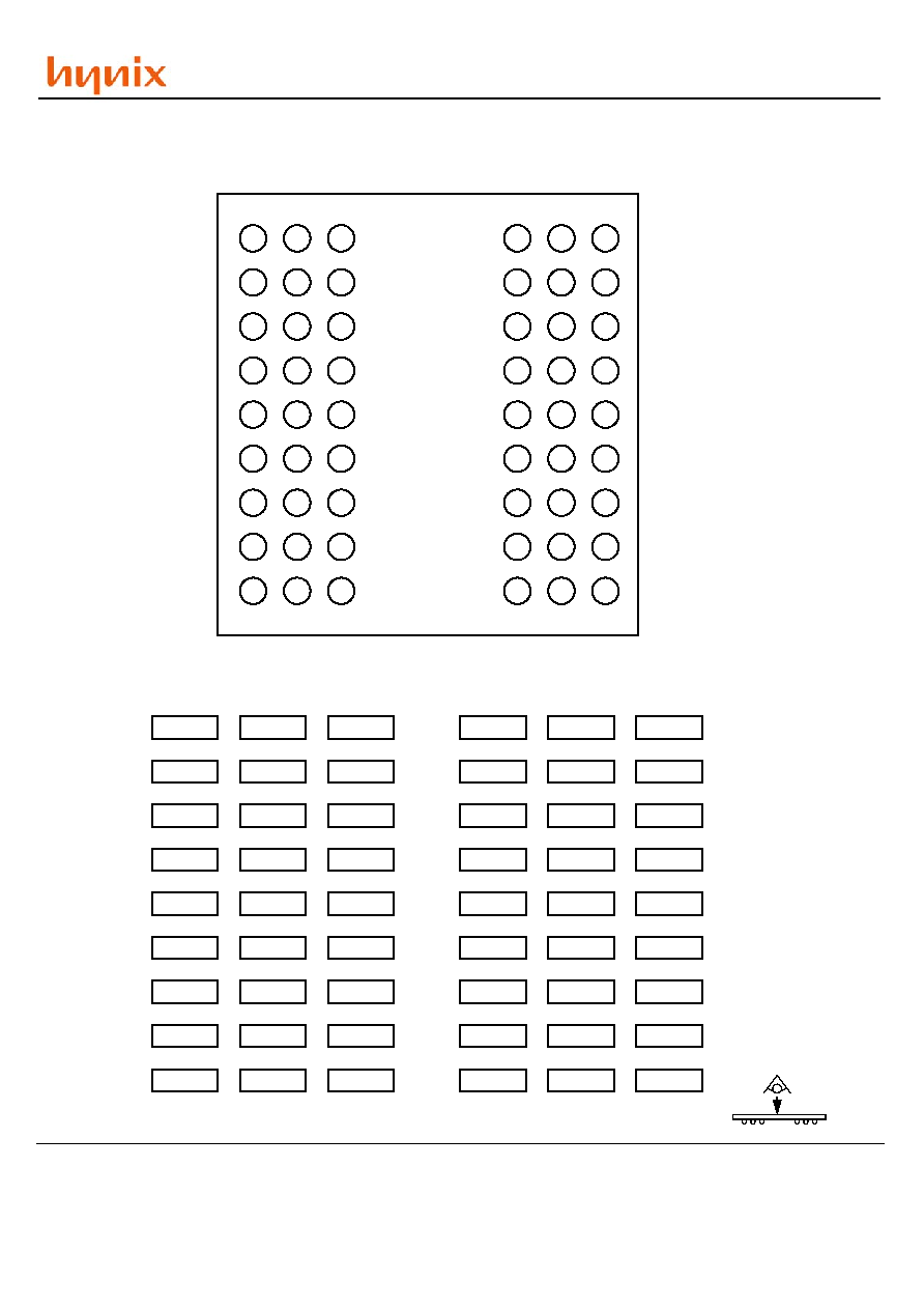
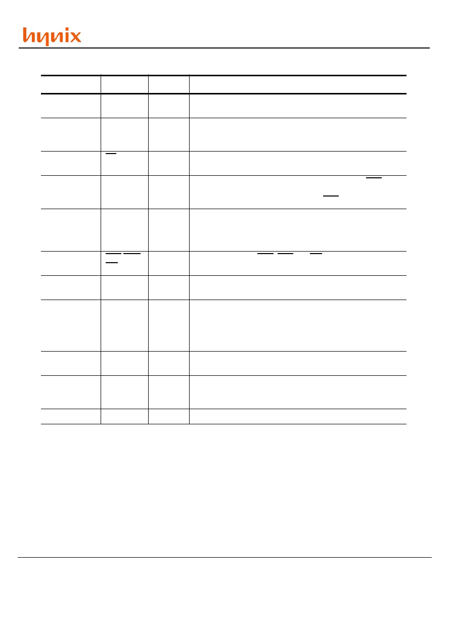
BALL DESCRIPTION
BALL OUT
SYMBOL
TYPE
DESCRIPTION
F2
CLK
INPUT
Clock : The system clock input. All other inputs are registered
to the SDRAM on the rising edge of CLK
F3
CKE
INPUT
Clock Enable : Controls internal clock signal and when deacti-
vated, the SDRAM will be one of the states among power
down, suspend or self refresh
G9
CS
INPUT
Chip Select : Enables or disables all inputs except CLK, CKE,
UDQM and LDQM
G7,G8
BA0, BA1
INPUT
Bank Address : Selects bank to be activated during RAS activ-
ity
Selects bank to be read/written during CAS activity
H7, H8, J8, J7,
J3, J2, H3, H2,
H1, G3, H9,
G2, G1
A0 ~ A12
INPUT
Row Address : RA0 ~ RA12, Column Address : CA0 ~ CA8
Auto-precharge flag : A10
F8, F7, F9
RAS, CAS,
WE
INPUT
Command Inputs : RAS, CAS and WE define the operation
Refer function truth table for details
F1, E8
UDQM,
LDQM
INPUT
Data Mask:Controls output buffers in read mode and masks
input data in write mode
A8, B9, B8,
C9, C8, D9,
D8, E9, E1,
D2, D1, C2,
C1, B2, B1, A2
DQ0 ~
DQ15
I/O
Data Input/Output:Multiplexed data input/output pin
A9, E7, J9, A1,
E3, J1
VDD/VSS
SUPPLY
Power supply for internal circuits
A7, B3, C7,
D3, A3, B7,
C3, D7
VDDQ/
VSSQ
SUPPLY
Power supply for output buffers
E2
NC
-
No connection