For technical questions, contact FunctionPAK@vishay.com
For marketing questions, contact FunctionPAK.marketing@vishay.com
www.vishay.com
19
FX5959G701
Vishay
Document Number: 10135
Revision 07-Jul-04
FEATURES
∑ Fully integrated Power LED driver
∑ High efficiency over large load range
∑ 100% duty cycle
∑ Power density - more than 450W/inch
3
∑ 1uA shutdown current
∑ Variable input voltage 2.5V to 6V (1Li+ or 3-cell NiCd or NiMH cells)
∑ Controlled output current
∑ Programmable PWM/PSM controls
∑ Low output ripple
∑ BGA construction
∑ Temperature range: - 40∞C to + 85∞C
∑ No external components required
∑ Output power 15W
∑ Maximum current 2.5A
∑ Short circuit protection
∑ Low profile
APPLICATIONS
∑ Bike lamps
∑ Headlights and flashlights
∑ Medical instrumentation
∑ General and emergency/alarm lighting
∑ Design and architectural lighting
∑ Interior and runway lights
∑ Outdoor accent lighting
∑ Household appliances
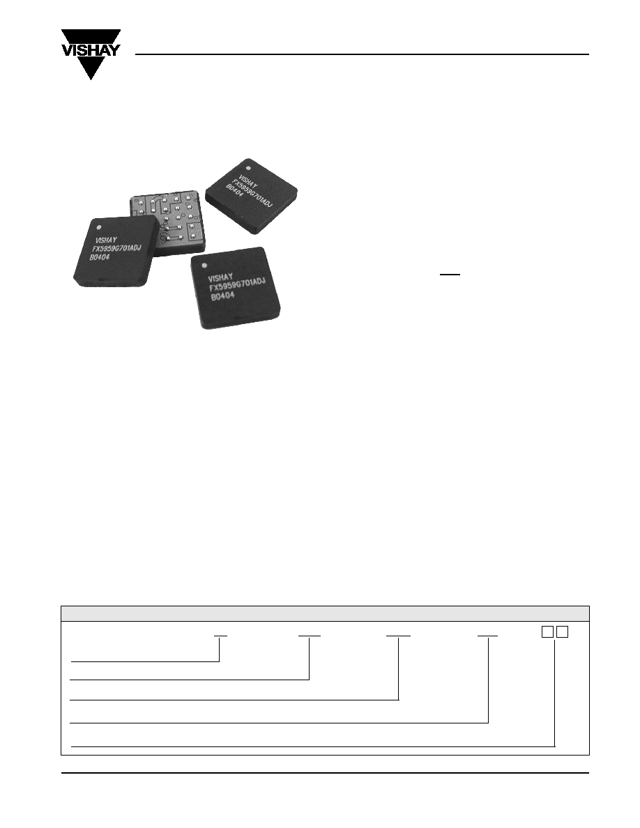
Power LED Driver the Smallest and Low Profile,
Constant Current Source 0 - 2.0A, 2.5V to 7V, with 450W/in
3
Power Density and High Efficiency
FX
5959
G701
ADJ
FUNCTION
SIZE
CIRCUIT IDENTIFIER
OUTPUT VOLTAGE - ADJ for adjustable version - self selectable output voltage. (see note below)
PACKAGING - B1 = 10pcs in bulk; B5 = 50pcs in bulk; T5 = 500pcs in 13" reel.
ORDERING INFORMATION
The Power LED Driver is dedicated for optimum
performance to drive Power LED's. FX5959 is a complete
system solution for all Power LED's with high current for
e.g. > 300 mA. The driver provides a constant current
without exceeding the applicable LED voltage to ensure the
specified LED load life time. The integrated Current Source
provides flexibility of utilizing various battery
configurations and chemistries such as NiCd, NiMH, or Li+
with input voltage range of 2.5v to 6v. An additional
flexibility is provided by using external resistors to adapt to
various voltage input levels and LED configurations. For ul-
tra-high efficiency, the Power LED Driver is designed to op-
erate in synchronous rectified PWM mode under full load
while transforming into externally controlled pulse-skipping
mode (PSM) under light load (for e.g. LED's with 20 to 200 mA).
The FX5959 Current Source is available in 25-ports BGA
package. In order to satisfy the stringent ambient
temperature requirements, the Current Source is designed
to handle the industrial temperature range of ≠40∞C to 85∞C.
* Note: for fixed output current please contact Function PAK@vishay.com

For technical questions, contact FunctionPAK@vishay.com
For marketing questions, contact FunctionPAK.marketing@vishay.com
Document Number: 10135
Revision 07-Jul-04
www.vishay.com
20
FX5959G701
Vishay
A
A
F
D
25
1
DIMENSIONS in inches [millimeters]
T
BGA
A
B
A
B
L
L
L
0.59 ± 0.01
[15 ± 0.25]
A
0.1 ± 0.01
[2.54 ± 0.25]
B
0.95 ± 0.01
[2.42 ± 0.25]
T
0.126 max
[3.2 max]
Ball Diameter
0.03 ± 0.001
[0.762 ± 0.025]
A
D
F
0.1 ± 0.01
0.03 ± 0.001
0.02 ± 0.001
[2.54 ± 0.25]
[0.8 ± 0.02]
[0.5 ± 0.02]
PIN
CONNECTION
4, 5
Vin
9, 14
SD*
10, 15
PWM/PSM*
20, 25
SYNC*
1-3, 7, 8,
GND
13, 18, 23
19, 24
R1
ext
21, 22
V
TP
16, 17
R0
ext
6, 11, 12
Load
PIN CONFIGURATION
UPPER SIDE
21 22 23 24 25
16 17 18 19 20
11 12 13 14 15
6 7 8 9 10
1 2 3 4 5
Note:
*must be connected to Vin.
RECOMMENDED PAD PATTERN in inches [millimeters]
Vin
SD
PWM/PSM
SYNC
GND
R1
R0
V
TP
V
L
R1
R0

For technical questions, contact FunctionPAK@vishay.com
For marketing questions, contact FunctionPAK.marketing@vishay.com
www.vishay.com
21
FX5959G701
Vishay
Document Number: 10135
Revision 07-Jul-04
PARAMETER
UNIT
CONDITION
MINIMUM
TYPICAL
MAXIMUM
Input
Voltage Range
V
DC
2.5
6.0
Quiescent Current
µA
PSM mode
200
Soft Start Time
ms
T
SS
for Vout = 6.0V
22
ms
T
SS
for Vout = 5.0V
22
ms
T
SS
for Vout = 3.3V
19
SD, PWM/PSM, SYNC
Logic High
V
V
H
2.4
Logic Low
V
V
L
0.8
Normal Mode
µA
I
DD
750
PSM Mode
µA
I
DD
250
Shutdown Mode
µA
I
DD
1
Shutdown Time
ms
T
SS
for Vout = 6.0V
15
ms
T
SS
for Vout = 5.0V
14
ms
T
SS
for Vout = 3.3V
14
Insulation
Test Voltage
V
AC
60Hz 60sec
750
Resistance
V
ISO
= 500V
DC
1 x 10
11
Leakage Current
nA
V
ISO
= 500V
DC
5
Output
(V
TP
-V
L
) I
OUT
W
at 25∞C ambient temperature
1.5
W
at 85∞C ambient temperature
0.8
Power
W
15
Voltage
V
DC
7
Current Tolerance
%
at 25∞C ambient temperature
± 10
Temp. Coefficient
%/∞C
0.03
Ripple and Noise
mVpp
DC to 20MHz
45
General
Package Weight
gr.
1.65
Oscillator
Frequency
KHz
670
SYNC Range
F
SYNC
/F
OSC
1.2
1.5
Temperature
Operation
∞C
- 40
+ 85
Storage
∞C
- 55
+ 125
Operating Junction Temp.
∞C
Tj
150
Thermal Impedance
∞C/W
D
*
JA
82
STANDARD ELECTRICAL SPECIFICATIONS
Note:
*W
D
= Power Dissipated
Fall Time
Rise Time
Rise Time (PWM mode): Vin = 3V; V
TP
= 3.3V; Iout = 2.5A
Fall Time (PWM mode): Vin = 3V; V
TP
= 3.3V; Iout = 2.5A

For technical questions, contact FunctionPAK@vishay.com
For marketing questions, contact FunctionPAK.marketing@vishay.com
Document Number: 10135
Revision 07-Jul-04
www.vishay.com
22
FX5959G701
Vishay
Fall Time
Rise Time
Rise Time (PWM mode): Vin = 4.5V; V
TP
= 5V; Iout = 2A
Fall Time (PWM mode): Vin = 4.5V; V
TP
= 5V; Iout = 2A
Rise Time (PWM mode): Vin = 5V; V
TP
= 6V; Iout = 1A
Fall Time (PWM mode): Vin = 5V; V
TP
= 6V; Iout = 1A
Rise Time (PWM mode): Vin = 3.5V; V
TP
= 5V; Iout = 2A
Fall Time (PWM mode): Vin = 3.5V; V
TP
= 5V; Iout = 2A
RIse Time (PWM mode): Vin = 3V; V
TP
= 3.3V; Iout = 2A
Fall Time (PWM mode): Vin = 3V; V
TP
= 3.3V; Iout = 2A

For technical questions, contact FunctionPAK@vishay.com
For marketing questions, contact FunctionPAK.marketing@vishay.com
www.vishay.com
23
FX5959G701
Vishay
Document Number: 10135
Revision 07-Jul-04
Fall Time
Rise Time
Rise Time (PWM mode): Vin = 4V; V
TP
= 6V; Iout = 1A
Fall Time (PWM mode): Vin = 4V; V
TP
= 6V; Iout = 1A
Rise Time (PWM mode): Vin = 3V; V
TP
= 3.3V; Iout = 1A
Fall Time (PWM mode): Vin = 3V; V
TP
= 3.3V; Iout = 1A
Rise Time (PWM mode): Vin = 4.5V; V
TP
= 5V; Iout = 1A
Fall Time (PWM mode): Vin = 4.5V; V
TP
= 5V; Iout = 1A
Rise Time (PWM mode): Vin = 3.5V; V
TP
= 5V; Iout = 1A
Fall Time (PWM mode): Vin = 3.5V; V
TP
= 5V; Iout = 1A