 | –≠–ª–µ–∫—Ç—Ä–æ–Ω–Ω—ã–π –∫–æ–º–ø–æ–Ω–µ–Ω—Ç: 440GP | –°–∫–∞—á–∞—Ç—å:  PDF PDF  ZIP ZIP |

4/1/03
PowerPC 440GP Embedded Processor Data Sheet
Page 1 of 64
Features
∑ PowerPC
440 processor core operating up to
500MHz with 32KB I- and D-caches
∑ On-chip 8 KB SRAM
∑ Selectable processor:bus clock ratios of 3:1,
4:1, 5:1, 5:2, 7:2
∑ Double Data Rate (DDR) Synchronous DRAM
(SDRAM) 32/64-bit interface operating up to
133MHz
∑ External Peripheral Bus for up to eight devices
with external mastering
∑ DMA support for external peripherals, internal
UART and memory
∑ PCI-X V1.0a interface (32 or 64 bits, up to
133MHz) with support for conventional PCI
V2.2
∑ Two Ethernet 10/100 Mbps half- or full-duplex
interfaces. Operational modes supported are
MII, RMII, and SMII.
∑ Programmable Interrupt Controller supports
interrupts from a variety of sources.
∑ Programmable General Purpose Timers (GPT)
∑ Two serial ports (16750 compatible UART)
∑ Two IIC interfaces
∑ General Purpose I/O (GPIO) interface available
∑ JTAG interface for board level testing
∑ Internal Processor Local Bus (PLB) runs at
DDR SDRAM interface frequency
∑ PowerPC processor boot from PCI memory
Description
Designed specifically to address high-end
embedded applications, the PowerPC 440GP
(PPC440GP) provides a high-performance, low
power solution that interfaces to a wide range of
peripherals by incorporating on-chip power
management features and lower power dissipation.
This chip contains a high-performance RISC
processor core, DDR SDRAM controller,8KB
SRAM, PCI-X bus interface, Ethernet interfaces,
control for external ROM and peripherals, DMA with
scatter-gather support, serial ports, IIC interface,
and general purpose I/O.
Technology: IBM CMOS SA-27E, 0.18
µ
m
(0.11 L
eff
), 5-layer metal
Package: 25mm, 552-ball Ceramic Ball Grid Array
(CBGA)
Power (estimated): Less than 4.0W. Less than
1.0 W in sleep mode
Supply voltages required: 3.3 V, 2.5V, 1.8V

PowerPC 440GP Embedded Processor Data Sheet
Page 2 of 64
4/1/03
Contents
Ordering and PVR Information . . . . . . . . . . . . . . . . . . . . . . . . . . . . . . . . . . . . . . . . . . . . . . . . . . . . . . . . . . . . 4
Address Maps . . . . . . . . . . . . . . . . . . . . . . . . . . . . . . . . . . . . . . . . . . . . . . . . . . . . . . . . . . . . . . . . . . . . . . . . . 5
PowerPC 440 Processor Core . . . . . . . . . . . . . . . . . . . . . . . . . . . . . . . . . . . . . . . . . . . . . . . . . . . . . . . . . . . . 8
Internal Buses . . . . . . . . . . . . . . . . . . . . . . . . . . . . . . . . . . . . . . . . . . . . . . . . . . . . . . . . . . . . . . . . . . . . . . . . . 8
PCI-X Interface . . . . . . . . . . . . . . . . . . . . . . . . . . . . . . . . . . . . . . . . . . . . . . . . . . . . . . . . . . . . . . . . . . . . . . . . 9
DDR SDRAM Memory Controller . . . . . . . . . . . . . . . . . . . . . . . . . . . . . . . . . . . . . . . . . . . . . . . . . . . . . . . . . 10
On-Chip SRAM . . . . . . . . . . . . . . . . . . . . . . . . . . . . . . . . . . . . . . . . . . . . . . . . . . . . . . . . . . . . . . . . . . . . . . . . 9
External Peripheral Bus Controller (EBC) . . . . . . . . . . . . . . . . . . . . . . . . . . . . . . . . . . . . . . . . . . . . . . . . . . . 10
Ethernet Controller Interface . . . . . . . . . . . . . . . . . . . . . . . . . . . . . . . . . . . . . . . . . . . . . . . . . . . . . . . . . . . . . 11
DMA Controller . . . . . . . . . . . . . . . . . . . . . . . . . . . . . . . . . . . . . . . . . . . . . . . . . . . . . . . . . . . . . . . . . . . . . . . 11
Serial Port . . . . . . . . . . . . . . . . . . . . . . . . . . . . . . . . . . . . . . . . . . . . . . . . . . . . . . . . . . . . . . . . . . . . . . . . . . . 11
IIC Bus Interface . . . . . . . . . . . . . . . . . . . . . . . . . . . . . . . . . . . . . . . . . . . . . . . . . . . . . . . . . . . . . . . . . . . . . . 11
General Purpose Timers (GPT) . . . . . . . . . . . . . . . . . . . . . . . . . . . . . . . . . . . . . . . . . . . . . . . . . . . . . . . . . . 12
General Purpose IO (GPIO) Controller . . . . . . . . . . . . . . . . . . . . . . . . . . . . . . . . . . . . . . . . . . . . . . . . . . . . . 12
Universal Interrupt Controller (UIC) . . . . . . . . . . . . . . . . . . . . . . . . . . . . . . . . . . . . . . . . . . . . . . . . . . . . . . . 12
JTAG . . . . . . . . . . . . . . . . . . . . . . . . . . . . . . . . . . . . . . . . . . . . . . . . . . . . . . . . . . . . . . . . . . . . . . . . . . . . . . . 13
Signal Lists . . . . . . . . . . . . . . . . . . . . . . . . . . . . . . . . . . . . . . . . . . . . . . . . . . . . . . . . . . . . . . . . . . . . . . . . . . 15
Signal Description . . . . . . . . . . . . . . . . . . . . . . . . . . . . . . . . . . . . . . . . . . . . . . . . . . . . . . . . . . . . . . . . . . . . . 39
Heat Sink Mounting Information . . . . . . . . . . . . . . . . . . . . . . . . . . . . . . . . . . . . . . . . . . . . . . . . . . . . . . . . . . 48
Test Conditions . . . . . . . . . . . . . . . . . . . . . . . . . . . . . . . . . . . . . . . . . . . . . . . . . . . . . . . . . . . . . . . . . . . . . . . 50
Spread Spectrum Clocking . . . . . . . . . . . . . . . . . . . . . . . . . . . . . . . . . . . . . . . . . . . . . . . . . . . . . . . . . . . . . . 52
DDR SDRAM . . . . . . . . . . . . . . . . . . . . . . . . . . . . . . . . . . . . . . . . . . . . . . . . . . . . . . . . . . . . . . . . . . . . . . . . 59
Initialization . . . . . . . . . . . . . . . . . . . . . . . . . . . . . . . . . . . . . . . . . . . . . . . . . . . . . . . . . . . . . . . . . . . . . . . . . . 61
Strapping . . . . . . . . . . . . . . . . . . . . . . . . . . . . . . . . . . . . . . . . . . . . . . . . . . . . . . . . . . . . . . . . . . . . . . . . . . . . 61
EEPROM . . . . . . . . . . . . . . . . . . . . . . . . . . . . . . . . . . . . . . . . . . . . . . . . . . . . . . . . . . . . . . . . . . . . . . . . . . . 61
Figures
PPC440GP Functional Block Diagram . . . . . . . . . . . . . . . . . . . . . . . . . . . . . . . . . . . . . . . . . . . . . . . . . . . . . . 5
25mm, 552-Ball CBGA Package . . . . . . . . . . . . . . . . . . . . . . . . . . . . . . . . . . . . . . . . . . . . . . . . . . . . . . . . . 14
Heat Sink Attached With Spring Clip . . . . . . . . . . . . . . . . . . . . . . . . . . . . . . . . . . . . . . . . . . . . . . . . . . . . . . 48
Heat Sink Attached With Adhesive . . . . . . . . . . . . . . . . . . . . . . . . . . . . . . . . . . . . . . . . . . . . . . . . . . . . . . . . 48
Timing Waveform . . . . . . . . . . . . . . . . . . . . . . . . . . . . . . . . . . . . . . . . . . . . . . . . . . . . . . . . . . . . . . . . . . . . . 51
Input Setup and Hold Waveform . . . . . . . . . . . . . . . . . . . . . . . . . . . . . . . . . . . . . . . . . . . . . . . . . . . . . . . . . . 54
Output Delay and Float Timing Waveform . . . . . . . . . . . . . . . . . . . . . . . . . . . . . . . . . . . . . . . . . . . . . . . . . . 54
DDR SDRAM Write Cycle Timing . . . . . . . . . . . . . . . . . . . . . . . . . . . . . . . . . . . . . . . . . . . . . . . . . . . . . . . . . 60
DDR SDRAM Read Cycle Timing . . . . . . . . . . . . . . . . . . . . . . . . . . . . . . . . . . . . . . . . . . . . . . . . . . . . . . . . . 60

PowerPC 440GP Embedded Processor Data Sheet
4/1/03
Page 3 of 64
Tables
System Memory Address Map . . . . . . . . . . . . . . . . . . . . . . . . . . . . . . . . . . . . . . . . . . . . . . . . . . . . . . . . . . . . 6
DCR Address Map . . . . . . . . . . . . . . . . . . . . . . . . . . . . . . . . . . . . . . . . . . . . . . . . . . . . . . . . . . . . . . . . . . . . . 7
Signals Listed Alphabetically . . . . . . . . . . . . . . . . . . . . . . . . . . . . . . . . . . . . . . . . . . . . . . . . . . . . . . . . . . . . 15
Signals Listed by Ball Assignment . . . . . . . . . . . . . . . . . . . . . . . . . . . . . . . . . . . . . . . . . . . . . . . . . . . . . . . . 33
Pin Summary . . . . . . . . . . . . . . . . . . . . . . . . . . . . . . . . . . . . . . . . . . . . . . . . . . . . . . . . . . . . . . . . . . . . . . . . 39
Signal Functional Description . . . . . . . . . . . . . . . . . . . . . . . . . . . . . . . . . . . . . . . . . . . . . . . . . . . . . . . . . . . . 40
Absolute Maximum Ratings . . . . . . . . . . . . . . . . . . . . . . . . . . . . . . . . . . . . . . . . . . . . . . . . . . . . . . . . . . . . . 47
Package Thermal Specifications . . . . . . . . . . . . . . . . . . . . . . . . . . . . . . . . . . . . . . . . . . . . . . . . . . . . . . . . . 47
Recommended DC Operating Conditions . . . . . . . . . . . . . . . . . . . . . . . . . . . . . . . . . . . . . . . . . . . . . . . . . . 49
Input Capacitance . . . . . . . . . . . . . . . . . . . . . . . . . . . . . . . . . . . . . . . . . . . . . . . . . . . . . . . . . . . . . . . . . . . . . 50
DC Power Supply Loads . . . . . . . . . . . . . . . . . . . . . . . . . . . . . . . . . . . . . . . . . . . . . . . . . . . . . . . . . . . . . . . 50
Clocking Specifications . . . . . . . . . . . . . . . . . . . . . . . . . . . . . . . . . . . . . . . . . . . . . . . . . . . . . . . . . . . . . . . . . 51
Peripheral Interface Clock Timings . . . . . . . . . . . . . . . . . . . . . . . . . . . . . . . . . . . . . . . . . . . . . . . . . . . . . . . . 53
I/O Specifications--All Speeds . . . . . . . . . . . . . . . . . . . . . . . . . . . . . . . . . . . . . . . . . . . . . . . . . . . . . . . . . . . 55
I/O Specifications--400, 466, and 500 MHz . . . . . . . . . . . . . . . . . . . . . . . . . . . . . . . . . . . . . . . . . . . . . . . . . 58
Strapping Pin Assignments . . . . . . . . . . . . . . . . . . . . . . . . . . . . . . . . . . . . . . . . . . . . . . . . . . . . . . . . . . . . . 61

PowerPC 440GP Embedded Processor Data Sheet
Page 4 of 64
4/1/03
Ordering and PVR Information
For information on the availability of the following parts, contact your local IBM sales office.
Each part number contains a revision code. This is the die mask revision number and is included in the part
number for identification purposes only.
The PVR (Processor Version Register) is software accessible and contains additional information about the
revision level of the part. Refer to the
PPC440GP User's Manual for details on the register content.
Order Part Number Key
Product
Name
Order Part Number
1
Processor
Frequency
Package
Rev
Level
PVR Value
JTAG ID
PPC440GP
IBM25PPC440GP-3CC400C
400 MHz
25mm, 552 CBGA
C
0x40120481
0x02052049
PPC440GP
IBM25PPC440GP-3CC400CZ
400 MHz
25mm, 552 CBGA
C
0x40120481
0x02052049
PPC440GP
IBM25PPC440GP-3CC400E
400 MHz
25mm, 552 CBGA
C
0x40120481
0x02052049
PPC440GP
IBM25PPC440GP-3CC400EZ
400 MHz
25mm, 552 CBGA
C
0x40120481
0x02052049
PPC440GP
IBM25PPC440GP-3CC466C
466 MHz
25mm, 552 CBGA
C
0x40120481
0x02052049
PPC440GP
IBM25PPC440GP-3CC466CZ
466 MHz
25mm, 552 CBGA
C
0x40120481
0x02052049
PPC440GP
IBM25PPC440GP-3CC500C
500 MHz
25mm, 552 CBGA
C
0x40120481
0x02052049
PPC440GP
IBM25PPC440GP-3CC500CZ
500 MHz
25mm, 552 CBGA
C
0x40120481
0x02052049
Notes:
1. Z at the end of the Order Part Number indicates a tape-and-reel shipping package. Otherwise, the chips are shipped in a tray.
IBM Part Number
IBM25PPC440GP-3CC500Ex
Package (CBGA)
Processor Speed
Grade 3 Reliability
Case Temperature Range
Revision Level
Shipping Package:
Blank = Tray
Z = Tape and reel
C = -40 ∞C to +85∞C
E = -40∞C to +105 ∞C
PowerPC 440GP Embedded Processor Data Sheet
4/1/03
Page 5 of 64
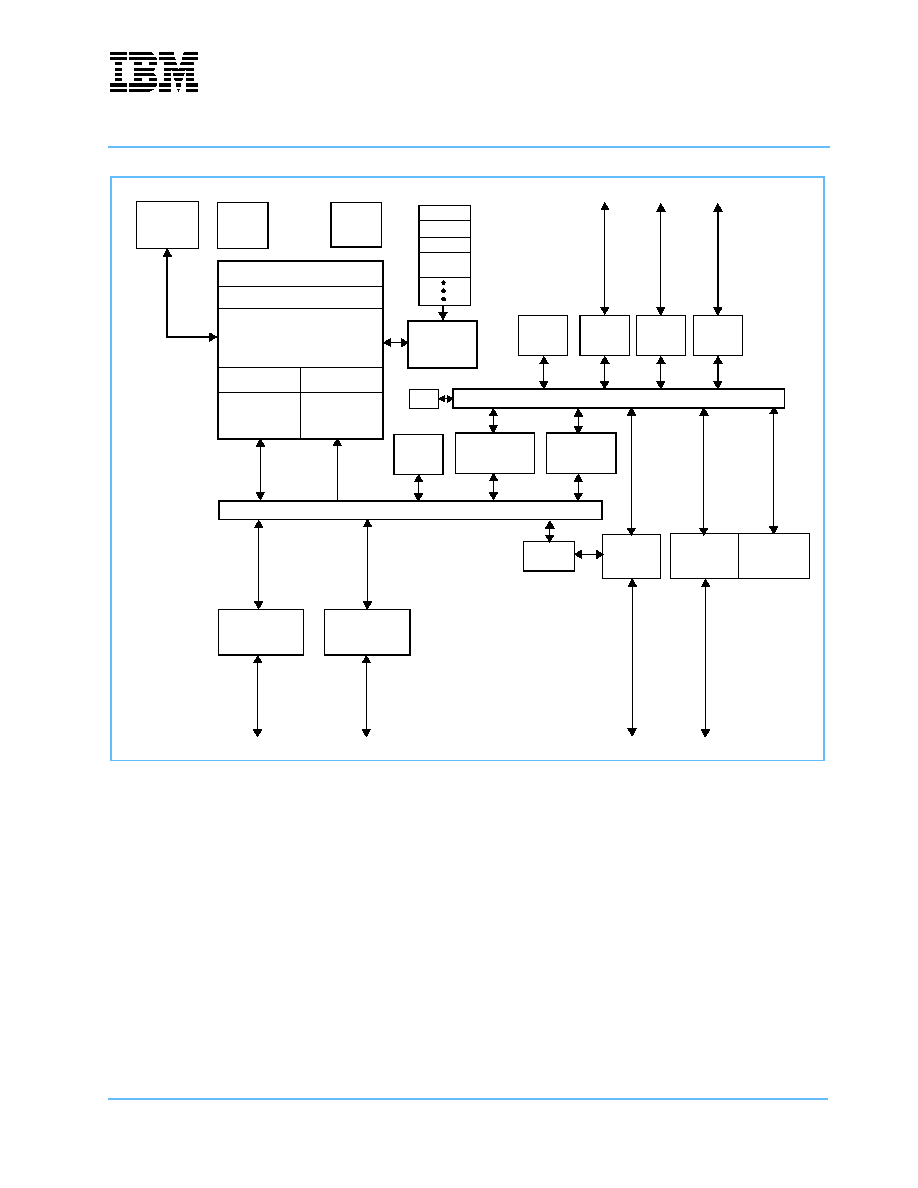
PPC440GP Functional Block Diagram
The PPC440GP is designed using the IBM Microelectronics Blue Logic
methodology in which major
functional blocks are integrated together to create an application-specific product (ASIC). This approach
provides a consistent way to create complex ASICs using IBM CoreConnect
Bus
Architecture.
Note: IBM CoreConnect buses provide:
∑ 128-bit PLB interfaces up to 133.33 MHz, 2.1 GB/s
∑ 32-bit OPB interfaces up to 66.66MHz, 266 MB/s
Address Maps
The PPC440GP incorporates two address maps. The first is a fixed processor system memory address map.
This address map defines the possible contents of various address regions which the processor can access.
The second address map is for Device Configuration Registers (DCRs). The DCRs are accessed by software
running on the PPC440GP processor through the use of mtdcr and mfdcr instructions.
Processor Core
DCR Bus
32KB
On-chip Peripheral Bus (OPB)
GPIO
IIC
UART
DMA
Bridge
Processor Local Bus (PLB)
DDR SDRAM
External
Bus
Controller
Controller
Clock
Control
Reset
Power
Mgmt
JTAG
Trace
Timers
MMU
Controller
OPB
Interrupt
Controller
Arb
32-bit addr
32-bit data
13-bit addr
32/64-bit data
External
Bus Master
Controller
Universal
I-Cache
32KB
D-Cache
(4-Channel)
133MHz max
66 MHz max
SRAM
8KB
PPC440
45 internal
13 external
PCI-X
Bridge
x2
x2
MAL
Ethernet
x2
133 MHz max
DCRs
1 MII
or
2 RMII
or
2 SMII
GP
Timers