
IBM Packet Routing Switch PRS28.4G
Version 1.7
Datasheet
�

Copyright and Disclaimer
Copyright International Business Machines Corporation 1999, 2000, 2001.
All Rights Reserved
Printed in the United States of America February 2001
The following are trademarks of
International Business Machines Corporation in the United States, or other coun-
tries, or both.
IBM
IBM logo
Other company, product and service names may be trademarks or service marks of others.
All information contained in this document is subject to change without notice. The products described in this docu-
ment are NOT intended for use in implantation or other life support applications where malfunction may result in injury
or death to persons. The information contained in this document does not affect or change IBM's product specifications
or warranties. Nothing in this document shall operate as an express or implied license or indemnity under the intellec-
tual property rights of IBM or third parties. All information contained in this document was obtained in specific environ-
ments, and is presented as an illustration. The results obtained in other operating environments may vary.
THE INFORMATION CONTAINED IN THIS DOCUMENT IS PROVIDED ON AN "AS IS" BASIS.
In no event will IBM be liable for damages arising directly or indirectly from any use of the information contained in this
document.
IBM Microelectronics Division
1580 Route 52, Bldg. 504
Hopewell Junction, NY 12533-6351
The IBM home page can be found at http://www.ibm.com
The IBM Microelectronics Division home page can be found at http://www.chips.ibm.com
prs28_title.04.fm
February 6, 2001
�

PRS28.4G
IBM Packet Routing Switch
prs28.04TOC.fm
February 6, 2001
Page 3 of 131
Contents
List of Figures ................................................................................................................ 7
List of Tables .................................................................................................................. 9
1. General Information .................................................................................................. 11
1.1 Features ......................................................................................................................................... 11
1.2 Description .................................................................................................................................... 11
1.3 Ordering Information .................................................................................................................... 12
1.4 Conventions .................................................................................................................................. 12
2. Architecture ............................................................................................................... 15
2.1 Functional Island ........................................................................................................................... 16
2.1.1 Sizing ..................................................................................................................................... 16
2.1.2 Output Queuing and Priorities ............................................................................................... 16
2.1.3 Flow Control .......................................................................................................................... 17
2.1.4 Multicast ................................................................................................................................ 17
2.1.5 Control Packets ..................................................................................................................... 17
2.1.6 Incoming Flow Process ......................................................................................................... 17
2.1.7 Incoming Flow Control ........................................................................................................... 17
2.1.8 Outgoing Flow Process ......................................................................................................... 18
2.1.9 Outgoing Flow Control ........................................................................................................... 18
2.1.10 Signaling .............................................................................................................................. 19
2.1.11 Internal Features ................................................................................................................. 19
2.1.12 Miscellaneous ...................................................................................................................... 20
2.2 Expansion Modes .......................................................................................................................... 22
2.2.1 Speed Expansion .................................................................................................................. 22
2.2.2 Port Expansion ...................................................................................................................... 23
3. Functional Description ............................................................................................. 25
3.1 Logical Interface ............................................................................................................................ 25
3.1.1 Physical Interface .................................................................................................................. 26
3.1.2 Packet Type ........................................................................................................................... 27
3.2 Header Format ............................................................................................................................... 30
3.2.1 Header Byte H0 - Packet Qualifier ........................................................................................ 30
3.2.2 Header Byte H1 and H2 ........................................................................................................ 32
3.2.3 Idle Packet Trailer Byte T ...................................................................................................... 33
3.3 Packet Reception .......................................................................................................................... 33
3.3.1 Master Input Port Operation .................................................................................................. 33
3.3.2 Slave Input Port Operation .................................................................................................... 34
3.3.3 Parity and CRC Errors ........................................................................................................... 34
3.3.4 Address Insertion ................................................................................................................... 35
3.4 Input Flow Control ........................................................................................................................ 35
3.4.1 Memory Threshold Exceeded Condition ............................................................................... 35
3.4.2 Programming the Memory Full Thresholds ........................................................................... 35
3.4.3 Output Queue Threshold Exceeded Condition ...................................................................... 36
3.4.4 Packet Reception Fairness .................................................................................................... 36

PRS28.4G
IBM Packet Routing Switch
Page 4 of 131
prs28.04TOC.fm
February 6, 2001
3.5 Output Queue Grant Signaling ..................................................................................................... 37
3.5.1 Adapter Transmission Rules .................................................................................................. 38
3.5.2 Flow Control Error .................................................................................................................. 38
3.6 Output Queues and Output Queue Priorities ............................................................................. 39
3.7 Shared Memory ............................................................................................................................. 39
3.7.1 Organization ........................................................................................................................... 39
3.7.2 Shared Memory Access by Local Processor ......................................................................... 39
3.8 Packet Transmission .................................................................................................................... 40
3.8.1 Output Port Servicing ............................................................................................................. 40
3.8.2 Idle Packet Transmission ....................................................................................................... 41
3.9 Send Grant ..................................................................................................................................... 42
3.10 Receive Filter ............................................................................................................................... 42
3.11 Port Disabling .............................................................................................................................. 43
3.12 Address Manager and Address Corruption .............................................................................. 43
3.13 Control Packets ........................................................................................................................... 43
3.13.1 Control Packet Reception .................................................................................................... 43
3.13.2 Control Packet Transmission ............................................................................................... 44
3.14 Speed Expansion ........................................................................................................................ 44
3.14.1 External Speed Expansion ................................................................................................... 44
3.14.2 Internal Speed Expansion .................................................................................................... 44
3.14.3 Packet Reception Window for Speed Expansion ................................................................. 45
3.14.4 Synchronization of Slave Device with Master Device .......................................................... 45
3.14.5 Master Slave Address Communication ................................................................................ 45
4. Programming Interface and Internal Registers ...................................................... 47
4.1 OCM Instruction/Status Mode ...................................................................................................... 47
4.1.1 OCM Instruction Register ....................................................................................................... 47
4.1.2 OCM Instruction Set ............................................................................................................... 47
4.1.3 OCM Response Register ....................................................................................................... 49
4.1.4 OCM Error Checking .............................................................................................................. 49
4.1.5 Operational Protocol .............................................................................................................. 50
4.2 OCM Scan Mode ............................................................................................................................ 50
4.2.1 Operational Protocol .............................................................................................................. 50
4.2.2 Scan String Access from OCM .............................................................................................. 51
4.3 Built In Self Test (BIST) ................................................................................................................. 51
4.3.1 Pseudo-Random Pattern Generator (PRPG) ......................................................................... 51
4.3.2 Multiple Input Signature Register (MISR) .............................................................................. 51
4.3.3 BIST Execution ...................................................................................................................... 52
5. Internal Registers ...................................................................................................... 54
5.1 Status Register .............................................................................................................................. 54
5.2 Application Register Definitions .................................................................................................. 56
5.2.1 Indirect Access of Memory Data and Look-Up Table ............................................................ 57
5.2.2 Register Formats ................................................................................................................... 57
5.2.3 Mode Register ........................................................................................................................ 58
5.2.4 Configuration Register 0 ........................................................................................................ 59
5.2.5 Configuration Register 1 ........................................................................................................ 61
5.2.6 Port Enable Register .............................................................................................................. 62
5.2.7 Output Queue Threshold Register ......................................................................................... 63

PRS28.4G
IBM Packet Routing Switch
prs28.04TOC.fm
February 6, 2001
Page 5 of 131
5.2.8 Shared Memory Threshold Register 0 ................................................................................... 64
5.2.9 Shared Memory Threshold Register 1 ................................................................................... 65
5.2.10 Mask Register ...................................................................................................................... 66
5.2.11 Synchronization Status and Hunt Register .......................................................................... 67
5.2.12 Sync Packet Transmit Register ........................................................................................... 68
5.2.13 CRC Port ID Register .......................................................................................................... 69
5.2.14 CRC Error Counter .............................................................................................................. 70
5.2.15 NoSignal Register ................................................................................................................ 71
5.2.16 Flow Control Violation Port ID Register ............................................................................... 72
5.2.17 Miscellaneous Status Register ............................................................................................ 73
5.2.18 Output Queue Status Registers 0-3 .................................................................................... 74
5.2.19 Look-Up Tables and Memory Row ...................................................................................... 75
5.2.20 Table Pointer Register ......................................................................................................... 76
5.2.21 Table Data Register ............................................................................................................. 77
5.2.22 Memory Row Address Register ........................................................................................... 78
5.2.23 Command Register .............................................................................................................. 79
5.2.24 Control Packet Destination Register .................................................................................... 80
5.2.25 Bit Map Filter Register ......................................................................................................... 81
5.2.26 Yellow Packet Received Register ........................................................................................ 82
5.2.27 PLL Configuration Register ................................................................................................. 83
5.2.28 Processor Access Registers ................................................................................................ 84
5.2.29 Processor Address Register ................................................................................................ 84
5.2.30 Processor Data Register ..................................................................................................... 85
5.2.31 BIST Data Register .............................................................................................................. 86
5.2.32 BIST Control Register .......................................................................................................... 87
6. Reset, Initialization, and Operation ......................................................................... 88
6.1 Clock and PLL ............................................................................................................................... 88
6.1.1 Internal PLL ........................................................................................................................... 88
6.1.2 External PLL .......................................................................................................................... 88
6.2 Reset .............................................................................................................................................. 88
6.2.1 Power-On-Reset Sequence and Clock Start OCM Event ..................................................... 88
6.2.2 Flush Reset and OCM_RESET Command ........................................................................... 89
6.2.3 nTRST Primary Input Reset .................................................................................................. 89
6.3 Initialization ................................................................................................................................... 89
6.4 DASL Initialization and Operation ............................................................................................... 90
6.5 Control Packet Reception and Transmission ............................................................................. 92
6.5.1 Control Packet Reception ...................................................................................................... 92
6.5.2 Control Packet Transmission ................................................................................................. 93
7. I/O Definitions and Timing ....................................................................................... 94
7.1 I/O Timing ..................................................................................................................................... 105
7.1.1 DASL Signals ...................................................................................................................... 105
7.1.2 OCM Interface Signals ........................................................................................................ 105
7.1.3 Master-Slave Speed Expansion Signals ............................................................................. 108
8. Packaging and Pin Information ............................................................................. 109
9. DASL Specification and Pico-Processor .............................................................. 124

PRS28.4G
IBM Packet Routing Switch
Page 6 of 131
prs28.04TOC.fm
February 6, 2001
10. Electrical Characteristics ...................................................................................... 125
11. Line Termination .................................................................................................... 128
11.1 HSTL ........................................................................................................................................... 128
11.2 DASL and SYS_CLK .................................................................................................................. 128
12. Internal RAM ABIST ............................................................................................... 130
13. References ............................................................................................................. 131
3. Revision Log ............................................................................................................ 131

PRS28.4G
IBM Packet Routing Switch
prs28.04LOF.fm
February 6, 2001
List of Figures
Page 7 of 131
List of Figures
Figure 1: Pinout ........................................................................................................................................... 13
Figure 2: Block Diagram .............................................................................................................................. 14
Figure 3: Speed Expansion Block Diagram ................................................................................................. 22
Figure 4: Single Stage Port Expansion Block Diagram ............................................................................... 24
Figure 5: Packet Format 1.77 Gb/s Port ...................................................................................................... 25
Figure 6: Packet Format for 3.54 Gb/s Port ................................................................................................ 25
Figure 7: Idle Packet Format ....................................................................................................................... 28
Figure 8: Input-side Grant Operation ........................................................................................................... 38
Figure 9: OCM Interface Signals Timing Diagram ..................................................................................... 105
Figure 10: OCM Signal Timing Diagram .................................................................................................... 106
Figure 11: SND_GRANT(n) ....................................................................................................................... 107
Figure 12: RCV_GRANT(n) ....................................................................................................................... 107
Figure 13: Q_FULL, Q_EMPTY, Q_SYNC Timing Diagram ..................................................................... 108
Figure 14: Package Physical Dimensions ................................................................................................. 109
Figure 15: HSTL Termination .................................................................................................................... 128
Figure 16: DASL Termination for Slave LUs ............................................................................................. 128
Figure 17: DASL Termination for Master LUs, Bits 2 and 3 ...................................................................... 129

PRS28.4G
IBM Packet Routing Switch
List of Figures
Page 8 of 131
prs28.04LOF.fm
February 6, 2001

PRS28.4G
IBM Packet Routing Switch
prs28.04LOT.fm
February 6, 2001
List of Tables
Page 9 of 131
List of Tables
Table 1: Speed Expansion Shared Memory Buffering Capacities ................................................................ 22
Table 2: Physical Bit Organization of a Port ................................................................................................. 27
Table 3: Packet Length and Logical Unit Length .......................................................................................... 29
Table 4: Header Byte H0 for Idle Packets .................................................................................................... 30
Table 5: Header Byte H0 for Data Packet (Bits 2 and/or 3
0), and Control Packet ................................... 30
Table 6: Data Packet Priority ........................................................................................................................ 31
Table 7: Bit Map Filter .................................................................................................................................. 31
Table 8: Header Byte 1 and 2 and Incoming Packet Bitmap ........................................................................ 32
Table 9: Header Byte 0 and 1 and Output queue grant ................................................................................ 32
Table 10: Byte Reordering via the Look-Up Table ....................................................................................... 41
Table 11: Shared Memory Reserved Address for Control Packets .............................................................. 44
Table 12: Port Combination in Internal Port Expansion ................................................................................ 45
Table 13: OCM Instruction Set Definitions ................................................................................................... 47
Table 14: Number of Instruction Bits Protected by Parity Bit ........................................................................ 49
Table 15: OCM Instruction Mode Sequence ................................................................................................ 50
Table 16: OCM Scan Mode Sequence ......................................................................................................... 50
Table 17: Simulated BIST Signatures .......................................................................................................... 53
Table 18: Status Register Bit Definitions ...................................................................................................... 54
Table 19: Application Register List ............................................................................................................... 56
Table 20: Master and Slave Memory Bank Addressing ............................................................................... 92
Table 21: Signal Definitions .......................................................................................................................... 94
Table 22: DBG_DATA Bus Definitions ....................................................................................................... 100
Table 23: I/O Summary .............................................................................................................................. 102
Table 24: DASL Interface Skew ................................................................................................................. 105
Table 25: OCM Signal Timing Values ........................................................................................................ 106
Table 26: SND_Grant Sampling Window Timing ....................................................................................... 107
Table 27: RCV_Grant Sampling Window Timing ....................................................................................... 107
Table 28: Q_FULL, Q_EMPTY, Q_SYNC Timing Values .......................................................................... 108
Table 29: Pin List, Sorted by Pin Name ...................................................................................................... 110
Table 30: Pin List, Sorted by Pin Number .................................................................................................. 117
Table 31: DASL Temperature Range ......................................................................................................... 124
Table 32: Instruction Memory in Processor Address Space ....................................................................... 124
Table 33: Absolute Maximum Ratings ........................................................................................................ 125
Table 34: Recommended Operating Conditions ........................................................................................ 126
Table 35: Electrical Characteristics for DASL I/Os ..................................................................................... 127
Table 36: Clocks ......................................................................................................................................... 127

PRS28.4G
IBM Packet Routing Switch
List of Tables
Page 10 of 131
prs28.04LOT.fm
February 6, 2001

prs28.04.fm
February 6, 2001
PRS28.4G
IBM Packet Routing Switch
General Information
Page 11 of 131
1. General Information
1.1 Features
� Non-blocking, self-routing, single-stage switch
� High Performance:
- 100 MHz to 111.1 MHz frequency operation
- 1.77 Gb/s throughput per port (16x16 config.)
- Up to 3.54 Gb/s throughput per port (8x8 con-
fig.)
- Up to 28.4 Gb/s single device aggregate
throughput
- Up to 56.8 Gb/s aggregate throughput with
speed expansion
� Serial data communication at 444 Mb/s, compli-
ant with the EIA/JEDEC JESD8-6 standard.
� Multicast support without packet duplication in
shared memory
� Dynamically shared output buffer (256 packets
of 64 to 80 bytes)
� Configurable number of traffic priorities (1 to 4)
with programmable output queue thresholds
and shared memory thresholds
� Configurable packet lengths of:
- 64 to 80 bytes (increment of four)
- 128 to 160 (increment of eight) with external
speed expansion only
� Serial processor interface (on-chip monitor)
� Packet header of three bytes, containing desti-
nation bit map, packet priority, switch redun-
dancy support information, all protected by a
parity bit
� Shared output buffer with total capacity of:
- 256 packets for a single chip
- 512 packets with external speed expansion
� Packet lossless switchover (scheduled
switchover) facility
� Reception on any input port of Control Packets
destined to the local processor
� Transmission of control packets from the local
processor to any output port
� Detection of link liveness by reception of specific
packets
� Programmable byte shuffling in outgoing
packets
� CMOS5S6 (0.35
�
m) technology: 3.3V compliant
TTL compatible I/O for low speed signals
� IEEE 1149.1 standard boundary scan to facili-
tate circuit board testing
1.2 Description
The IBM Packet Routing Switch PRS28.4G is the
first in a family of second generation switching
devices designed for high performance, non-
blocking fixed length packet switching. Its modularity
enables development of scalable switch fabrics of
aggregate bandwidth from 28.4Gb/s to 227.2 Gb/s.
The PRS28.4G receives packets on 16 input ports
and routes them to one or more of 16 output ports
based on bit map information carried in the packet
header. Each port operates at 1.77 Gb/s, resulting in
a single device throughput of 28.4 Gb/s. This data
speed is achieved by implementing, in one device,
two 16 by 16 sub-switch elements, running at 888
Mb/s per port and organized internally in speed
expansion mode. In addition, 444 Mb/s serial data
communication provides, over two differential pairs,
the necessary bit rate per island.
Quality of service support is provided through four
levels of packet priority. The architecture supports
flow control, based on a grant mechanism, and
provides programmable thresholds, one per priority.
Scalability of speed is achieved by external speed
expansion. Two devices operate in parallel (one as
master, the other as slave) to form a 16 by 16 switch
element at 3.54 Gb/s per port. Scalability of ports is
provided by single stage port expansion, which
allows the number of ports on the switch fabric to be
increased.
No synchronization is required between input ports.
However, packets on a given port are always
received or transmitted at fixed periodicity equal to
the packet length.

PRS28.4G
IBM Packet Routing Switch
General Information
Page 12 of 131
prs28.04.fm
February 6, 2001
1.3 Ordering Information
1.4 Conventions
Throughout this document, standard IBM notation is used: bits and bytes are numbered in ascending order
from left to right. Thus the Most Significant Bit (MSB) has the lowest number and the Least Significant Bit
(LSB) has the highest number:
The use of overbars, for example RESET, designates signals that are active low.
Decimal, hexadecimal, and binary numbers are used in this document and represented as follows:
Decimal:
12345.67
Hexadecimal:
0x"ABCD" or ABCD'x'
Binary:
`000'b
Part Number
Description
IBM3221L0572
IBM Packet Routing Switch
MS
B
LS
B
0
1
2
3
4
5
6
7
8
9
10 11 12 13 14 15 16 17 18 19 20 21 22 23 24 25 26 27 28 29 30 31

PRS28.4G
IBM Packet Routing Switch
prs28.04.fm
February 6, 2001
General Information
Page 13 of 131
Figure 1: Pinout
(Refer to
Pin List, Sorted by Pin Number
on page 117 for names of all pins).
AE
AD
AC
AB
AA
0Y
0W
0V
0U
0T
0R
0P
0N
0M
0L
0K
0J
0H
0G
0F
0E
0D
0C
0B
0A
01 02 03 04 05 06 07 08 09 10 11 12 13 14 15 16 17 18 19 20 21 22 23 24 25
VDD
GND
No Connect
Signal Pin

PRS28.4G
IBM Packet Routing Switch
General Information
Page 14 of 131
prs28.04.fm
February 6, 2001
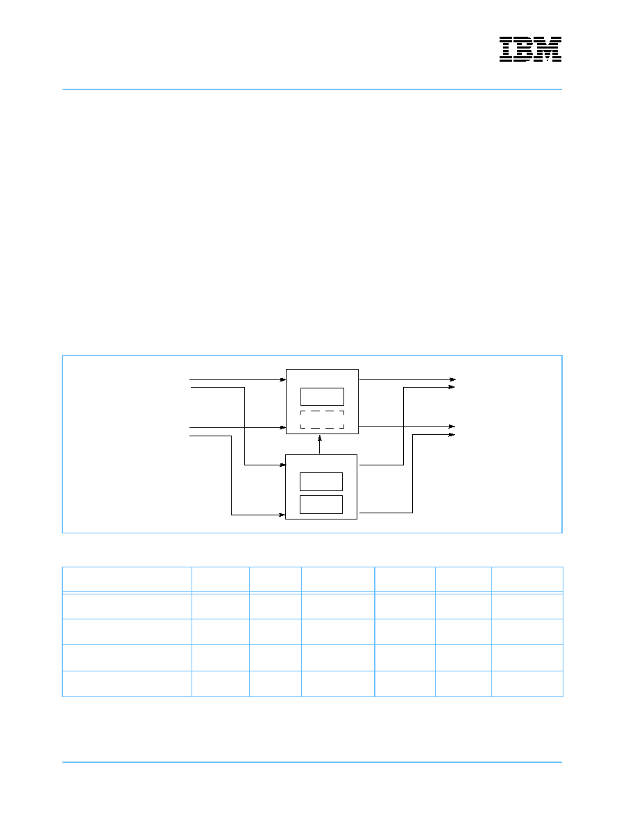
Figure 2: Block Diagram
Input
Controller
0
Input
Controller
15
Shared Memory
512 Rows
Slave
Shared Memory
512 Rows
Master
Address Manager
Output Queue 0
Output Queue 15
Output
Controller
0
Output
Controller
15
Ou
t
p
u
t
Qu
e
u
e
R
e
ad
M
a
na
ge
r
Ou
t
p
u
t
Qu
e
u
e
A
c
ce
ss
Ma
na
ge
r
of 512 positions

PRS28.4G
IBM Packet Routing Switch
prs28.04.fm
February 6, 2001
Architecture
Page 15 of 131
2. Architecture
The PRS28.4G incorporates two 888 Mb/s, per-port, self-routing sub-switch elements and a control section
that is common to both.
Each 1.77 Gb/s port therefore carries two data streams, one master and one slave, each at 888 Mb/s. The
master stream carries the data packet header bytes, followed by some packet payload bytes. The slave
stream carries only payload bytes.
The input controllers examine the headers of incoming Data Packets and check the data integrity, using a
parity bit on the header bytes. Valid Data Packets are then stored in the shared memory, and their storage
addresses, along with the packet priority and bit map, are further processed by a centralized output queue
access manager. These addresses are enqueued into FIFO queues, one per output port and per priority,
according to the packet priority and bit-map field. Data Packets are then transmitted, one at a time according
to their place in the output queues, with the restriction that high priority packets always overtake lower priority
packets.
Multicast packets are processed the same way. A multicast packet is stored only once in the shared buffer,
while its address is enqueued in all output queues indicated by its bit map field. A multicast packet is trans-
mitted on the indicated outputs according to its position in each output queue, not necessarily at the same
time on all outputs.
A central address manager maintains a pool of free shared-buffer addresses and provides new store
addresses to the input controllers. Once a packet is transmitted, its address is returned to the address
manager. The address manager also keeps track of the number of outputs still holding each address, since
one address can be copied multiple times for multicast packets. Once this reaches zero, the address is
returned to the free address pool.
The shared memory is organized as two banks, one master and one slave, each consisting of 512 rows of 20
bytes, with one write port and one read port. Access to the shared memory is performed one input and output
port at a time. 16 to 20 bytes are transferred at each access, depending on the packet length. A central
sequencer grants shared memory access to the input and output ports, in round robin. This sequencer cycle
is equal, in byte cycles, to the number of data bytes stored at every access in one memory row. It is defined
as an integer between 16 and 20, such that packet length is a multiple of this integer. All cycles have equal
length. Without speed expansion or with speed expansion and packet length greater than 128 bytes, an LU is
received in two cycles of equal length. In speed expansion and packet length smaller than 128 bytes, it takes
only one cycle to receive an LU.
Data flow is controlled using a grant mechanism. Grants are given to the input interface of the attached
device to allow packets to be transmitted. Similarly, the output interface of the attached device provides
grants to each output port to enable packet transmission. On the input side of the switch, output queue
grants, which reflect the status of the output queues, and memory grants, for the status of the shared
memory, are provided. One output queue grant is provided per output and per priority. The output queue
manager maintains a counter for each output queue, which indicates the total number of packets enqueued
for that output, regardless of priority. Four programmable output queue thresholds are also provided, one for
each priority. All output counters are compared to those four thresholds once per sequencer cycle. If an
output counter value is less than the threshold, the corresponding grant is set. Otherwise, it is cleared. Simi-
larly, a counter keeps track of the total number of packets in the shared memory. Four programmable shared
memory thresholds are also provided, one for each priority. This counter is compared once per sequencer
cycle to those four thresholds to generate the memory grants. An input interface island is only allowed to

PRS28.4G
IBM Packet Routing Switch
Architecture
Page 16 of 131
prs28.04.fm
February 6, 2001
transmit a packet when it has received the output queue grants for the packet's destination, in addition to the
memory grant for the packet priority. On the output side, a send grant is provided to each output port, regard-
less of priority.
Control Packets can be received on any input ports and are passed one at a time to the local processor. A
control packet address queue allows buffering of up to 16 control addresses. Also, control packets can be
transmitted by the local processor on any set of output ports. Control Packets do not carry a priority and are
always transmitted on one output before any other enqueued Data Packets. Due to the slow nature of the
local processor access compared to the packet data traffic rate, Control Packet transmission is infrequent
and does not impact the performance of high priority traffic.
An On-Chip Monitor (OCM) provides a serial interface to a local processor for programming application regis-
ters and accessing control packets.
A high speed serial interface is used to minimize the number of pins and to provide direct access over an
extended distance. Two pairs of differential lines running at 444 Mb/s are provided for each master and slave
byte stream. Therefore, each port is composed of four differential lines. On the input side, the serial interface
provides deserialization of one 2.25 ns bit stream into a 9ns nibble stream of four bits. On the output side, a
9ns nibble stream is serialized into a 2.25 bit stream. For each stream, two nibbles are grouped to form a
byte. Data is transmitted with a known clock, such that only bit-phase alignment and packet alignment have to
be performed. There is a picocode mechanism that compensates for a skew between nimble of
�
1 clock
cycle between serial links belonging to the same port within the same device. The hardware scheduler
compensates for up to
�
2 clock cycles of skew between two devices in external speed expansion.
The following sections describe the architecture and features of the PRS28.4G from a black box perspective.
The internal structure of the device is not described. The first part describes the functional island of the
PRS28.4G architecture, its elementary building block. The second section describes the PRS28.4G speed
expansion mode.
2.1 Functional Island
2.1.1 Sizing
The PRS28.4G basic functional island is 16 input ports by 16 output ports. Each port runs at 0.8 Gb/s. The
PRS28.4G is a self-routing switch element with fixed packet length shared memory. Its shared memory has a
buffering capacity of 512 rows of 20 bytes.
The internal controller is managed by a sequencer, with a cycle value of 16 to 20 byte clocks (boundaries
included). The lower bound is given by the number of supported ports, and the upper bound by the maximum
row length of the shared memory. The island controller allows the handling of logical units (LU) of 16 to 20
bytes (in steps of 1 byte), or 32 to 40 bytes (in steps of 2 bytes). An LU is the part of a packet that one island
processes. The shared memory organization allows storage of 512 LUs of 16 to 20 bytes, or 256 LUs of 32 to
40 bytes.
2.1.2 Output Queuing and Priorities
Queuing is provided for each output port. Packets from each output are organized into four logical queues of
different priority. For each logical queue, packets are organized into a First In First Out (FIFO) queuing struc-
ture.

PRS28.4G
IBM Packet Routing Switch
prs28.04.fm
February 6, 2001
Architecture
Page 17 of 131
Incoming packets are sorted by priority when stored, according to a priority flag they carry. The highest
priority is represented by 0 and the lowest by 3. Packets are transmitted on a given output with the highest
available priority, always overtaking the lower priorities.
2.1.3 Flow Control
Flow control is provided by the output queue, as well as for the entire shared memory.
One threshold value is associated with all logical queues (of each output). Each output queue has one unique
counter. The total number of packets in all four logical queues of one output is compared to the threshold
value of a given priority, in order to provide flow control for that output priority.
In addition, one counter keeps track of the total number of packets in shared memory. The shared memory
also has four thresholds, one per priority. The total number of packets in shared memory is compared to
these threshold values for each priority, regardless of the output destination of the packets.
2.1.4 Multicast
The internal architecture of the island allows for packets, physically stored once in shared memory, to be
multicasted to multiple outputs. A multicast packet is transmitted on the output ports according to the FIFO
structure of each destination output queue (not necessarily at the same time on all ports). Multicast packets
can only have one priority for all of its destinations.
2.1.5 Control Packets
Support is provided for receiving packets destined to a local processor, and for transmitting packets
constructed by a local processor. These packets are known as Control Packets.
A 16-position FIFO queue is provided for incoming control packets (no priority is involved).
2.1.6 Incoming Flow Process
Each incoming packet carries information about the physical output addresses (output port) of its destina-
tions, the logical address (priority) per output, or all zero (identification as a control packet).
The island controller allows one packet, corresponding to one input, to be processed and stored at a time.
Inputs are visited once per sequencer cycle. When the input on which a packet arrives is visited by the island
controller, the packet data is stored once in the shared memory. The address of this location is placed in the
logical queues (specified by its priority) of all of its destination outputs according to its priority. At the same
time, the shared memory counter and the output queue counters of its destination are incremented.
If an incoming packet is marked as a control packet, it is also stored in shared memory. Its address is then
placed in a control packet queue, and an interrupt is sent to the local processor. An incoming control packet
can only be received if fewer than 16 control packets are present in the control packet queue. Otherwise, the
packet is discarded and a flag is raised.
2.1.7 Incoming Flow Control
Flow control of incoming packets is provided by grants which are authorizations for the attached adapter to
transmit a packet. Grants are provided separately for each output port and for each priority of a port. An
output queue grant for a priority is provided whenever the total packet count for an output (regardless of

PRS28.4G
IBM Packet Routing Switch
Architecture
Page 18 of 131
prs28.04.fm
February 6, 2001
priority) is below the output priority threshold. It is removed whenever this count exceeds the threshold value
(no hysteresis). Grants are also provided for the shared memory for each priority. The shared memory grant
(memory grant) for a given priority is provided whenever the total packet count in shared memory is below the
shared memory priority threshold. It is removed whenever this count exceeds the threshold value (no hyster-
esis).
An adapter is only allowed to transmit a packet when it has the memory grant for the packet priority as well as
the output queue grants for the destination logical outputs. For multicast packets, the adapter is allowed to
transmit a packet if it has the memory grant for the packet priority, regardless of output queue grants.
Incoming packets also carry a drop flag. This flag allows packet discard at the input of the island whenever
the memory grant and/or output queue grants are removed before the packet is received from the attached
adapter (due to the latency in grant update). The grant information used by the input controllers to decide to
drop a packet is updated once every sequencer cycle, providing fairness among all inputs.
Finally, an anti-streaming function is provided at the input controllers to detect badly behaving adapters.
When an adapter sends a packet to an output priority for which the output queue grant or memory grant have
not been given in the past eight packet cycles, the packet is discarded and an interrupt is raised. For multicast
packets, the same mechanism is applied, but it takes only the memory grants into consideration.
2.1.8 Outgoing Flow Process
In each of the four logical output queues, control packets and Data Packets are transmitted in the following
order:
1. Control Packets
2. Priority 0 packets
3. Priority 1 packets
4. Priority 2 packets
5. Priority 3 packets
This order cannot be changed. Packets of higher priority overtake packets of lower priority.
Control Packets are constructed by the local processor and can be transmitted one at a time to multiple
outputs The control packets take precedence over any other packet present in the shared memory.
2.1.9 Outgoing Flow Control
Flow control at the output is also provided by send grants (one per output), regardless of priority. A packet on
a given output can only be transmitted if the send grant is provided for that output.

PRS28.4G
IBM Packet Routing Switch
prs28.04.fm
February 6, 2001
Architecture
Page 19 of 131
2.1.10 Signaling
LU data is passed in and out of the island, one byte per clock cycle, for each input and output port, at a rate of
0.88 Gb/s.
The first byte of a packet, either incoming or outgoing, is called the Qualifier byte and carries information
about:
� Packet priority
� Packet identification
� Packet filtering support
� Drop flag
� Parity bit over the three byte header
2.1.10.1 Idle Packets
When no Data Packets are available on a port, fill-up (empty) packets, called Idle Packets, are transmitted.
The inputs recognize these packets by their packet identification, and they are not stored. Outputs automati-
cally generate Idle Packets also, when no Control Packets or Data Packets of any priority are available.
2.1.10.2 Input
For incoming Data Packets, the second and third bytes provide the address of the packet destination, in the
form of a bit map. Each bit of these two bytes is associated with an output port. A bit set to 1 in the bit map
indicates that the packet is to be routed to the corresponding port. This bit map field can point to multiple
outputs.
An incoming packet is interpreted as a Control Packet when the entire bit map field is set to 0.
2.1.10.3 Output
The second and third bytes of outgoing packets carry the grant status of all output ports. This grant status is
used by the receiver of the other adapter to make a decision on Data Packet transmission, according to the
incoming flow control scheme presented above. This grant status is referred to as an output queue grant.
On a given packet, the output queue grant field carries the status of all logical queues of the same priority.
Consecutive packets carry the grant status for the different priorities, in a cyclic order. The synchronization of
this cycle is provided by the packet numbering field contained in the outgoing Idle Packets.
2.1.11 Internal Features
2.1.11.1 Packet Filtering
A packet filtering function is provided on the switch island inputs in order to decide whether or not to receive
packets for certain destinations. According to the packet filtering field in the qualifier byte, the incoming
packet bit map is either logically ORed with a specified mask (its complement value) or not masked at all.
There is one mask for all 16 inputs.

PRS28.4G
IBM Packet Routing Switch
Architecture
Page 20 of 131
prs28.04.fm
February 6, 2001
2.1.11.2 Line Interface and Synchronization
Data are transmitted on the physical lines two bits at a time, at a rate four times that of the internal byte clock.
Each bit is carried by a differential pair at a speed of 444 Mb/s. Both the transmitting and receiving devices
run with the same byte clock.
Link synchronization is provided by a training sequence of special Idle Packets, called Sync Packets. When
sync packets are transmitted on a port, the receiving port can perform bit phase alignment of the incoming
data, as well as packet alignment. The format of these sync packets is such that they are recognized by the
receiving end as valid packets, and provide bit transitions on the physical line to allow for phase recovery. A
sync packet LU is entirely composed of `CC' bytes, except for the last byte which is `33'.
One data byte is carried over two differential pairs. One pair carries all even numbered bits, and the other one
all odd numbered bits. This converts the `CC' sync packet bytes into 0 and 1 bit transitions on the physical
lines.
2.1.11.3 Link Integrity
Link integrity is provided by a CRC field, placed in the last byte of all Idle Packet LUs. The 8-bit CRC is the
checksum of all bits carried over a port since the previous Idle Packet ended. Thus, when multiple Data
Packets are transmitted, followed at some time by an Idle Packet, the CRC of this Idle Packet covers all
previous Data Packets. This provides a measure of the link quality for fault isolation.
2.1.11.4 Packet Numbering
In order to extract the output queue grant information that is multiplexed in the second and third bytes of
outgoing packets, Idle Packets carry a packet numbering field. This field is equal to the value of the priority of
the grant status being carried by the current Idle Packets.
The number of packet cycles required to carry the output queue grant for all priorities is equal to the number
of priorities. This output queue grant cycle repeats itself as long as non-sync packets are transmitted. The
output queue grant cycle always starts with the lowest priority number and ends with the highest.
2.1.12 Miscellaneous
2.1.12.1 Receive Grants
A receive grant function is provided on device pins as a means to block packet reception for specific outputs.
This function allows the implementation of packet lossless switchover for simple switch systems. It cannot be
combined with the packet lossless switchover mechanism provided by colored packets. When a receive grant
is asserted, reception of Data Packets in the corresponding output queue is enabled. When a receive grant is
disasserted no incoming packets are stored in the corresponding output queue, regardless of their bit map.
2.1.12.2 Send Grants
Send grant pins are provided to control the outgoing flow. They indicate to the output controllers when
packets are allowed to be transmitted.

PRS28.4G
IBM Packet Routing Switch
prs28.04.fm
February 6, 2001
Architecture
Page 21 of 131
2.1.12.3 Colored Packet
Idle Packets and Data Packets also carry a color, either blue or red. Color packets are used to provide
support for packet lossless switchover.
Some Idle Packets carry a yellow color. The reception of a yellow Idle Packet on a given input is logged into a
register accessible by the local processor. Yellow packets can only be transmitted by the local processor.
Yellow packets are used as link liveness messages.
2.1.12.4 Control Packets
Data Packets for which the bit map field is 0 are detected as control packets and are passed to the local
processor via a dedicated queue. The first bit map byte of an incoming packet is overwritten by the input port
number on which the packet is received.
2.1.12.5 Queue Full
Queue-full information is also provided directly by the island. Sixteen bits carry all logical port full statuses, by
multiplexing the information of all priorities of a given port over one bit. At a given time, all 16 bits carry the full
status for the same priority, for all output queues. All priorities rotate, from the lowest number to the highest,
in a cyclic manner, while the change from one priority to the next only occurs after four byte cycles. An extra
bit indicates when all 16 queue-full bits carry priority 0, and is used to synchronize to this cycle.
2.1.12.6 Queue Empty
Queue-empty information is also provided by a 16-bit bus, for all logical output queues. The information multi-
plexing and timing is identical to the queue-full bits.
2.1.12.7 Look-Up Table
The lookup table is a facility that allows permutation of the bytes of outgoing packets. Only the first 16 bytes
can be permuted among each other or overwritten by one of the 16 bytes. One table is provided for all output
ports.
PRS28.4G
IBM Packet Routing Switch
Architecture
Page 22 of 131
prs28.04.fm
February 6, 2001
2.2 Expansion Modes
2.2.1 Speed Expansion
The PRS28.4G device is internally composed of two islands operating in speed expansion. It is a 16 x 16
shared-buffer device, with port speed of 1.77Gb/s. Each port is composed of two byte streams, one corre-
sponding to the master island, one to the slave island.
The device supports two-way speed expansion, that is, two devices can be combined to increase the port
speed to 3.2Gb/s. Supported packet lengths range from 64 to 80 bytes, in increments of four. However, when
two devices operate in speed expansion, packets of length 128 to 160, in increments of eight, are also
supported.
Note: The PRS28.4G implementation allows for only two (2) devices to be combined in external speed
expansion.
Speed expansion allows multiple devices to be connected in parallel to increase the port speed while keeping
the number of ports constant, as shown in the
Speed Expansion Block Diagram
.
In each case, the LU size seen by one island (either the master or the slave island of one device) is equal to
the packet length divided by the speed expansion factor (port speed divided by the island port speed of 0.88
Gb/s)
Figure 3: Speed Expansion Block Diagram
Table 1: Speed Expansion Shared Memory Buffering Capacities
Speed Expansion Mode
Switch
Configuration
Gb/s per
port
Packet Length
(bytes)
LU Size
(bytes)
Buffering
(packets)
Speed
Expansion Factor
Single device, no internal speed
expansion
16 x 16
1.77
64 - 80
32 - 40
256
2
Single device, with internal speed
expansion
8 x 8
3.54
64 - 80
16 - 20
256
4
Two devices speed expanded,
no internal speed expansion
16 x 16
3.54
64 - 80
16 - 20
512
4
Two devices speed expanded,
no internal speed expansion
16 x 16
3.54
128 - 160
32 - 40
256
4
Slave
Buffer
Control
16 Outputs
16 Inputs
Sync + Address
Master
Buffer
Control

PRS28.4G
IBM Packet Routing Switch
prs28.04.fm
February 6, 2001
Architecture
Page 23 of 131
2.2.1.1 External Speed Expansion
When multiple islands are running in speed expansion, one is master and the others are slaves. The master
device is the one which receives the byte stream containing the qualifier byte, bit map, and output queue
grant. The master device also performs packet routing and queuing. The slave devices only receive data
bytes, and do not perform any packet routing and queuing. The address of packets in shared memory is
provided by the master, and is the same for all devices. Furthermore, the slave devices' internal sequencers
are all synchronized on the master sequencer in order to transmit the LUsat the same time on a given port.
LUs of a packet incoming on a port have to arrive at all devices within a two-byte interval.
2.2.1.2 Internal Speed Expansion
Ports of one island can also be paired to double the port speed while reducing the number of input and output
ports to eight. Each pair of ports is built of one master port and one slave port, which have exactly the same
functions as the ports of master or slave islands in external speed expansion.
2.2.2 Port Expansion
Port expansion allows multiple islands to be interconnected in parallel, in a single stage, in order to increase
the number of physical ports, while keeping the port speed constant.
An external function must be provided to:
� Duplicate incoming packets and insert the correct bit map used by each island
� Merge traffic from different islands
The same external function can also instruct an island to transmit by controlling the send grants, according to
the queue-empty status, for instance.
Port expansion can be combined with speed expansion (internal and/or external) to increase port speed and
the number of ports at the same time.

PRS28.4G
IBM Packet Routing Switch
Architecture
Page 24 of 131
prs28.04.fm
February 6, 2001
.
Figure 4: Single Stage Port Expansion Block Diagram
Buffer
Control
Buffer
Control
Buffer
Control
Buffer
Control
32 Outputs
32 Inputs

PRS28.4G
IBM Packet Routing Switch
prs28.04.fm
February 6, 2001
Functional Description
Page 25 of 131
3. Functional Description
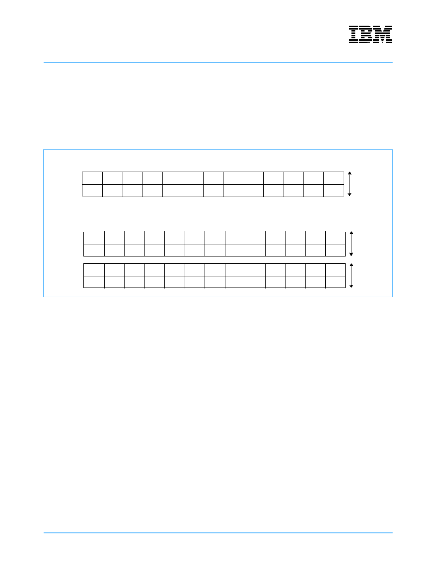
3.1 Logical Interface
As described in
Expansion Modes
on page 22, an PRS28.4G device consists of two switch islands running in
speed expansion. This leads to packet data being carried over an input or output port in two byte streams of
888 Mb/s, one related to the master island, and the other one to the slave island. Each byte stream carries
Logical Units (LU). An LU is a set of bytes belonging to the same packet and which are sent over one stream.
Depending on the expansion mode and packet length, an LU has a length L of 16 to 20 bytes or 32 to 40 (in
step of 2) bytes.
As represented in the figure below, the master LU always carries the packet routing information, or header
bytes, indicated by H0, H1 and H2.
When running in either internal or external speed expansion, two ports are grouped to form a 3.54Gb/s port.
Depending on the port and chip configuration, a 1.77Gb/s port can run either as a master port or a slave port:
� The master port is composed of two streams, one master, which carries the packet header information
and data bytes, and one slave, which carries data bytes only.
� The slave port is composed of two slave streams, which carry data bytes only.
The LUs of a packet are always transmitted or received at the same time on both streams of a port. Further-
more, the LUs of successive packets are transported one after the other, with no gap between packets.
Figure 5: Packet Format 1.77 Gb/s Port
Figure 6: Packet Format for 3.54 Gb/s Port
H0
H1
H2
D
D
D
D
D
D
D
D
D
D
D
D
D
D
D
D
D
D
D
D
D
W0
W1
W2
W3
W4
W5
W6
W(L-1)
D
D
. . .
. . .
. . .
Master LU
Slave LU
16 Bits
H0
H1
H2
D
D
D
D
D
D
D
D
D
D
D
D
D
D
D
D
D
D
D
D
D
W0
W1
W2
W3
W4
W5
W6
W(L-1)
D
D
. . .
. . .
. . .
Master LU
Slave LU
16 Bits
D
D
D
D
D
D
D
D
D
D
D
D
D
D
D
D
D
D
D
D
D
D
D
. . .
. . .
Master LU
Slave LU
16 Bits
Master Port
Slave Port
D
D
D

PRS28.4G
IBM Packet Routing Switch
Functional Description
Page 26 of 131
prs28.04.fm
February 6, 2001
3.1.1 Physical Interface
Within the device, an LU is transported in a stream of bytes at 111.1 MB/s. Externally, it is transported over
two bit streams of 444 Mb/s each. At chip-pin level, each bit stream interface is differential and complies with
the JEDEC JESD8-6 standard (HSTL).
Data bits are transferred across devices at a known frequency, and no companion clock is required.
However, bit-phase alignment is performed during the link synchronization phase.
The interface between the 9 ns and the 2.25 ns domains is handled by a data line interface, the Data Aligned
Serial Link (DASL).
� On the input side, the DASL deserializes the two bit streams into one byte stream. It also performs the
link synchronization to allow bit phase alignment and packet alignment.
� On the output side, the DASL serializes the byte stream into two bit streams.
An internal pico-processor (M3) performs the synchronization of all lines on all ports. A synchronization algo-
rithm running on the pico-processor performs the bit-phase alignment and packet alignment of all ports during
the synchronization phase (see
DASL Specification and Pico-Processor
on page 124). The synchronization
algorithm is downloaded into an internal instruction memory and is delivered along with the module. See
DASL Specification and Pico-Processor
on page 124 for more information.

PRS28.4G
IBM Packet Routing Switch
prs28.04.fm
February 6, 2001
Functional Description
Page 27 of 131
During serialization and deserialization, a one byte stream is split into two bit streams, one carrying the even
bits, and the other the odd bits. Thus, a port consists of four differential pairs. The information and bit order
that each pair carries is given in the table below.
Note: The MASTER stream is carried by bits 2 and 3, and the SLAVE stream by bits 0 and 1.
This bit grouping guarantees bit transitions to perform the phase alignment during synchronization on SYNC
packets.
3.1.2 Packet Type
A packet can be one of the following types:
� A Data Packet that contains user data to be switched from input to output.
� A Control Packet that is used to communicate with the local processor.
� An Idle Packet that does not contain user data. Idle Packets are sent on a link when no data packet are
available, or to perform link synchronization.
3.1.2.1 Data Packets and Control Packets
Data Packets carry user data and Control Packets carry information for local processor communication. The
figure
Packet Format 1.77 Gb/s Port
on page 25 shows the format of a data and control packet without speed
expansion. A packet consists of 16-bit words, divided into a master stream and a slave stream.
The figure
Packet Format for 3.54 Gb/s Port
on page 25 shows the Data and Control Packet format with
speed expansion, either internal or external. In those configurations, the packet is transported over two
different ports, either in the same device or in separate devices, in four LUs. The master port receives the
master LU and a slave LU, and the slave port receives two slave LUs.
Data Packets have a priority that ranges from 0 (highest) to 3 (lowest). In addition, they also carry filtering
(color) information used for switchover support.
Control Packets do not have priority, but they carry filtering (color) information.
Table 2: Physical Bit Organization of a Port
Differential Pair
Information Carried
Bit Order
Data_0_Q and Data_0_QN
even number bits of the slave byte stream
b0 b2 b4 b6 of slave byte
Data_1_Q and Data_1_QN
odd number bits of the slave byte stream
b1 b3 b5 b7 of slave byte
Data_2_Q and Data_2_QN
even number bits of the master byte stream
b0 b2 b4 b6 of master byte
Data_3_Q and Data_3_QN
odd number bits of the master byte stream
b1 b3 b5 b7 of master byte
PRS28.4G
IBM Packet Routing Switch
Functional Description
Page 28 of 131
prs28.04.fm
February 6, 2001
3.1.2.2 Idle Packets
The format of an Idle Packet without speed expansion (normal mode) is identical to data packet formats,
except that an Idle Packet contains two trailer-bytes in the last word of the packet.
Idle Packet format with speed expansion is similar to the data packet format for a 3.54 Gb/s port, except for
the trailer-bytes at the end of the packet.
Like Data Packets, Idle Packets also carry color information. However, in this case the color information is for
signaling (such as liveness messages, or to identify link synchronization packets, called Sync packets), in
addition to switchover support.
The payload bytes of nonsync Idle Packets - shown as `D' in the above two figures - are not processed and
are therefore irrelevant. However, in order to allow for dynamic phase alignment for the link interface receiver,
6 payload bytes are `CC'. All bytes of a non-sync Idle-packet LU transmitted by the PRS28.4G have the value
`00', with the following exceptions:
� Bytes 6 to 11 are all 0x`CC'.
� Byte 5 of a slave LU is 0x`07'.
� The last byte contains the trailer CRC.
� For a master LU, the header is defined according to the following sections.
3.1.2.3 Sync Packet
Sync packets are special types of Idle Packets, which allow link synchronization by providing bit transition
and packet delineation.
In accordance with the above definition of an Idle Packet, a Sync packet LU has all bytes equal to `CC',
except for the last byte, the trailer CRC byte, which is `33'.
The bit organization by the physical interface provides on a given differential pair, a sequence of `A', followed
by a `5'. This bit sequence provides the necessary bit transition while the `A to 5' transition allows for packet
delineation.
Figure 7: Idle Packet Format
H0
H1
H2
D
D
D
D
D
D
D
D
D
D
D
D
D
D
D
D
T
D
D
D
T
W0
W1
W2
W3
W4
W5
W6
W(L-1)
D
D
. . .
. . .
. . .
Master LU
Slave LU
16 Bits
Normal Mode
H0
H1
H2
D
D
D
D
D
D
D
D
D
D
D
D
D
D
D
D
T
D
D
D
T
W0
W1
W2
W3
W4
W5
W6
W(L-1)
D
D
. . .
. . .
. . .
Master LU
Slave LU
16 Bits
D
D
D
D
D
D
D
D
D
D
D
D
D
D
D
D
T
D
D
D
T
D
D
. . .
. . .
Slave LU
Slave LU
16 Bits
Master Port
Slave Port
D
D
D
Speed Expansion Mode

PRS28.4G
IBM Packet Routing Switch
prs28.04.fm
February 6, 2001
Functional Description
Page 29 of 131
3.1.2.4 Logical Unit Lengths
As mentioned previously, an LU is the part of a packet transported over one 0.8Gb/s stream. The table below
lists, for all speed expansion modes, all possible LU lengths and their corresponding packet lengths, as well
as the total packet buffering provided.
All packets received and transmitted by the switch have the same length.
Table 3: Packet Length and Logical Unit Length
Speed Expansion Mode
Switch Configuration
Gb/s Per Port
Packet Length
(Bytes)
LU Size
(Bytes)
Total Buffering
(packets)
Single device, no internal speed
expansion
16 x 16
1.77
64
68
72
76
80
32
34
36
38
40
256
Single device, with internal speed
expansion
8 x 8
3.54
64
68
72
76
80
16
17
18
19
20
256
Two devices speed expanded, no
internal speed expansion
16 x 16
3.54
64
68
72
76
80
16
17
18
19
20
512
Two devices speed expanded, no
internal speed expansion
16 x 16
3.54
128
136
144
152
160
32
34
36
38
40
256

PRS28.4G
IBM Packet Routing Switch
Functional Description
Page 30 of 131
prs28.04.fm
February 6, 2001
3.2 Header Format
3.2.1 Header Byte H0 - Packet Qualifier
3.2.1.1 Parity Bit
The parity bit is an even parity calculated on the first three bytes of the header. Even parity assures that the
resulting number of `1' in the three byte header is even. This ensures that the SYNC cell has a valid header.
3.2.1.2 Reserved Bits
Reserved bits pass through the device unmodified.
Table 4: Header Byte H0 for Idle Packets
(Bits 2 and 3
0)
Packet Type
Bit Position
0
1
2
3
4 and 5
6 and 7
Color bit
(1)
Parity
(1)
0
0
Color bits
(2)
Grant Priority
bits (2)
Blue Idle Packet
0
r
0
0
0 0
g g
Red Idle Packet
0
r
0
0
0 1
g g
Yellow Idle Packet
0
r
0
0
1 0
x x
Sync Packet
1
1
0
0
1 1
0 0
Reserved
1
1
1
0
r
r
r
r
0
0
0
0
0
0
0
0
0 0
0 1
1 0
1 1
x x
x x
x x
x x
Key:
x
value = 0 or 1
r
even parity bit on entire header (H0, H1, H2)
gg
value of grant sync bits (ignored for received packets - value = `00'
Table 5: Header Byte H0 for Data Packet
(Bits 2 and/or 3
0),
and Control Packet
(Bits 2 and/or 3
0; H1 and
H2
0)
Packet Type
Bit Position
0
1
2
3
4
5 and 6
7 and 8
Reserved
(1)
Parity
(1)
Active Bit
(1)
Backup Bit
(1)
Drop Bit
(1)
Reserved
(1)
Priority
(2)
Red Data/Control Packet
x
r
0
1
d
x
p p
Yellow Data/Control
Packet
x
r
1
0
d
x
p p
Blue Data/Control
Packet
x
r
1
1
d
x
p p
Key:
x
value = 0 or 1
r
even parity bit on entire header (H0, H1, H2)
gg
value of grant sync bits (ignored for received packets - value = `00'

PRS28.4G
IBM Packet Routing Switch
prs28.04.fm
February 6, 2001
Functional Description
Page 31 of 131
Data Packets will be transmitted in order of priority. A Control Packet is always transmitted before Data
Packets.
3.2.1.3 Active and Backup Bits
The Active and Backup bits are used to determine how the Bit Map Filter Mask is applied to the Bit Map Desti-
nation Address (header bytes H1 and H2) and to determine the traffic type (Red or Blue) of Data Packets.
The Bit Map Filter is a programmable register. The resulting masked destination bit map is used by the
PRS28.4G to route the packets to the appropriate destination(s), or to ignore the packet if the resulting bit
map is all zeros. Control Packet detection is performed before the Bit Map Filter is applied to the bit map
contained in the packet header.
3.2.1.4 Drop Bit
Incoming packets with the drop bit set will be dropped by the PRS28.4G when the number of packets in the
destination output queue and/or the shared memory has exceeded the programmable thresholds for the
corresponding priority. For multicast packets, the packet is dropped only if the shared memory threshold is
crossed. The output queue full information is updated once every sequencer cycle, so all input controllers see
the same output queue status in within a cycle.
When the drop bit is clear, the packet will not be dropped by the PRS28.4G due to either output queue or
shared memory thresholds.
3.2.1.5 Grant Priority Bits
The grant priority bits are defined only for Idle Packets transmitted by the PRS28.4G. For received packets,
this field is not examined (its value is `xx'). For transmitted packets, these bits encode the content of a fly
wheel counter, which characterize the priority of the inband output queue grant information (see next section)
stored in header bytes H1 and H2. The coding of bits gg is identical to the Data Packet priority listed in s
above.
Table 6: Data Packet Priority
(Ignored for Control Packets)
Priority Bits (p p)
Priority Level
0 0
Highest
0 1
Medium-high
1 0
Medium-low
1 1
Lowest
Table 7: Bit Map Filter
Active Bits
Backup Bits
Bit Map Filter
Data/Control Packet Color
0
0
Idle Packet.
n/a
0
1
Packet bit map is bit wise ANDed with bit wise complement of bit
map filter.
red
1
0
Packet bit map is bit wise ANDed with bit map filter.
red
1
1
Packet bit map is used unfiltered.
blue

PRS28.4G
IBM Packet Routing Switch
Functional Description
Page 32 of 131
prs28.04.fm
February 6, 2001
Yellow Idle Packets at the egress are considered as Data Packets and therefore do not carry grant priority
bits.
3.2.2 Header Byte H1 and H2
3.2.2.1 Received Packet: Bitmap
Header Bytes H1 and H2 of a received packet carry the destination bit map of the packet. Header Byte H1
carries destination information for output ports 0 through 7, and Header Byte H2 caries destination informa-
tion for output ports 8 through 15.
For Control Packets, the entire bit map field is set to `0'. Header Byte H2 is ignored for internal speed expan-
sion.
3.2.2.2 Transmitted Packet: Inband Output Queue Grant Information
Depending on the setting of the Flow Control Enable bit in Configuration Register 0, Header Bytes H1 and H2
provide inband access to the output queue grant information (this access is also provided on device pins).
Using the inband information assumes that it is the same device that transmits and receives packets on the
port.
When flow control is enabled, Header Bytes H1 and H2 carry the output queue grant. The output queue grant
is the grant information given to devices connected to the input ports. This information indicates the status of
the output queues and controls whether or not to transmit packets to the PRS28.4G. This information is
carried for all 16 output ports at the same time for a given priority. Consecutive packets, either idle or data
packet, carry a different priority, cycling from 0 to the highest priority value enabled. For instance, when two
priorities are enabled, it takes two packets to transmit the output queue grant information.
When all four priorities are enabled, the output queue grant information is transmitted in a cycle of four
packets. However, if the Three Threshold Enable bit is set in Configuration Register 0, the cycle is reduced to
3, and grants for priorities 0, 1, and 2 only are sent. It is then assumed that thresholds 2 and 3 are
programmed with the same value.
To synchronize the input interface device fly wheel counter with the inband output queue grant, the priority
value for which the output queue grant is transmitted is carried in the Priority Grant bits of the H0 Packet
Qualifier Byte of Idle Packets. Since inband grant priority is transmitted in cycles of consecutive packets,
priority synchronization is performed on Idle Packets only, and this information is not provided for Data
Packets. However, grant information is always transmitted.
Table 8: Header Byte 1 and 2 and Incoming Packet Bitmap
Bit:
0
1
2
3
4
5
6
7
Header Byte H1
Port:
0
1
2
3
4
5
6
7
Header Byte H2
Port:
8
9
10
11
12
13
14
15
Table 9: Header Byte 0 and 1 and Output queue grant
Bit
0
1
2
3
4
5
6
7
Header Byte H1
Output Queue:
0
1
2
3
4
5
6
7
Header Byte H2
Output Queue:
8
9
10
11
12
13
14
15

PRS28.4G
IBM Packet Routing Switch
prs28.04.fm
February 6, 2001
Functional Description
Page 33 of 131
H2 is set to 0x`FF' for internal speed expansion.
When the Flow Control Enable bit of Configuration Register 0 is not set, bytes H1 and H2 are identical to
bytes H1 and H2 of the received header.
3.2.3 Idle Packet Trailer Byte T
The Trailer Byte is only defined for Idle Packets. For the other packet types, the Trailer Byte contains user
data. The Trailer Byte contains an eight-bit CRC checksum value. The trailer CRC of a byte stream is calcu-
lated over all the bytes sent over that stream since the last Idle Packet CRC byte.
The CRC encoding is defined by the generating polynomial X8+X4+X3+X2+1. The initial value for CRC
calculation is programmable via an 8-bit CRC Init field in Configuration Register 1. The initial CRC value is
chosen so that the resulting trailer CRC of a Sync packet equals 0x'33' for all LU lengths. The CRC Init values
are given in the chapter describing Configuration Register 1.
When an Idle Packet is received, the CRC is verified. In case of an error, it is reported via an interrupt, when
not masked.
3.3 Packet Reception
3.3.1 Master Input Port Operation
Packets are received on an input asynchronously with the packets on the other inputs. When a start of packet
is expected, a master input port performs the following actions:
� The packet header is analyzed and the various fields are extracted from the header. The entire packet is
ignored if the header parity is incorrect. The error is reported via CRC Error interrupt and, if not masked,
the main interrupt is asserted. Also, the global CRC Error counter is incremented.
� If the header parity is correct and the received packet is not a sync packet, the packet color is extracted.
When the packet type is yellow (which is only possible for Idle Packets), bit n in the Yellow Register is set
(where n is the number of the input port).
Further actions depend on the packet type and are described in the following sections.
3.3.1.1 Idle Packet
In external speed expansion, the slave is informed that an Idle Packet has arrived. The Trailer Byte is verified.
If there is a CRC error, it is reported via the CRC Error interrupt and, if not masked, the main interrupt is
asserted. The global CRC Error counter is also incremented. No further action is taken for Idle Packets (not
stored in shared memory).

PRS28.4G
IBM Packet Routing Switch
Functional Description
Page 34 of 131
prs28.04.fm
February 6, 2001
3.3.1.2 Data Packet
� The packet is ignored if:
- The packet destination output ports are all disabled, or
- The packet cannot be stored in the packet memory. This is a flow control error and will be reported via
the Flow Control Violation interrupt. This error can only occur if the adapter does not follow the mem-
ory grant information. If the interrupt is not masked, the main interrupt is asserted.
� With speed expansion, if the packet is discarded, the slave input is informed that the incoming packet is
invalid. If the packet is accepted, the slave port receives the packet address from the master port.
3.3.1.3 Control Packet
� The packet is only received if the number of currently enqueued control packets does not exceed the fixed
threshold of 16; otherwise the control packet is ignored. With speed expansion, if the packet is not
received, the slave port is informed that the incoming packet is invalid. If the packet is received, the slave
port receives the packet address from the master port.
� When 16 control packets are already enqueued, the next control packet is discarded.
3.3.2 Slave Input Port Operation
When a start of packet is expected, a slave input port receives control information from the master port. For
each received packet this can be one of the following:
� An Idle Packet is received. The Trailer Byte is then verified. If a CRC error is detected, it is reported via
the CRC Error interrupt. The CRC Error Counter is also incremented. If the error is not masked, the main
interrupt is asserted.
� The incoming data packet is invalid. The packet is then ignored.
� The incoming data packet is valid. The packet is then stored in the packet memory at the address
received from the master port.
If both the slave and master port receive an Idle Packet, and the master port informs the slave port to ignore
the Idle Packet as a result of a header parity error, the slave will ignore the Trailer Byte in the Idle Packet.
3.3.3 Parity and CRC Errors
The detection of header parity errors and trailer CRC errors is reported via the CRC Error interrupt, and if not
masked, generates a main interrupt. Both type of errors also cause the CRC Error Counter to increment.
These interrupts are generated by the device that detects the error. In external speed expansion, the master
device reports header parity errors and trailer CRC errors for data on its input ports, and the slave device
reports trailer CRC errors for data on its input ports.

PRS28.4G
IBM Packet Routing Switch
prs28.04.fm
February 6, 2001
Functional Description
Page 35 of 131
3.3.4 Address Insertion
The input port number is inserted in header byte H1 of incoming Control Packets as follows:
The address insertion field is defined as a 5 bit field. However, in the PRS28.4G bit 3 is forced to 0.
3.4 Input Flow Control
The PRS28.4G continuously maintains shared memory and output queue status information. This status
information is periodically transmitted via the memory grants and output queue grants for flow control to
adapters which are connected to the PRS28.4G inputs.
Flow control is used to signal the adapter that it should stop transmitting packets when the packet memory
threshold is exceeded for the packet-priority or when an output queue threshold is exceeded for the packet
priority.
3.4.1 Memory Threshold Exceeded Condition
There are four programmable memory-full thresholds, one for each packet priority. These thresholds can be
used to prevent packets of a specific priority from using the entire packet memory. When the total number of
allocated memory locations exceeds the threshold value, the corresponding memory grant signal is cleared. It
is set whenever the total number of allocated locations is less than the threshold value.
The four memory-full thresholds must be programmed in decreasing order. That is, the memory-full threshold
for priority 0 must be greater than or equal to the memory-full threshold for priority 1, which in turn must be
greater than or equal to memory-full threshold for priority 2. Consequently, when memory-full threshold 0 is
exceeded, the other memory-full thresholds are also exceeded.
The memory-full information is available on device pins (MEM_GRANT).
3.4.2 Programming the Memory Full Thresholds
The memory-full threshold 0 should be programmed to:
NumberOfPackets - (16 * MasterGrantDelay) - ControlPacketLocations - 32.
32 addresses are reserved by the Input Controller and should be subtracted from the total number of
packets (either 256 or 512 depending whether speed expansion is off or on).
NumberOfPackets is the total packet storage available in shared memory, given in
Speed Expansion
Shared Memory Buffering Capacities
on page 22.
MasterGrantDelay is the reaction delay endured by the Memory grant pin information, calculated in LUs.
The PRS28.4G component of this delay is one LU time. The transmission and processing time of the
Memory Grant by the adapter must be added to this value.
Reserved
0
Input Port
Number
0
1
2
3
4
5
6
7

PRS28.4G
IBM Packet Routing Switch
Functional Description
Page 36 of 131
prs28.04.fm
February 6, 2001
ControlPacketLocations represents the 16 locations that are reserved for Control Packet reception, if
necessary.
3.4.3 Output Queue Threshold Exceeded Condition
There are four programmable output queue-full thresholds, one for each packet priority. All output queues
use the same threshold per priority. These thresholds can be used to:
� Prevent packets of a certain priority and destined to a specific output from using the entire packet
memory.
� Prevent packets of a certain priority from consuming too much output queue memory space (in relation to
packets of a higher priority).
When the total number of addresses, regardless of priorities, in an output queue exceeds a priority threshold,
the corresponding output queue grant is cleared. It is set whenever the total number of addresses in the
output queue is below the threshold value.
3.4.4 Packet Reception Fairness
Two fairness mechanisms are implemented to guarantee that, on the average, each input has an equal
chance of receiving a packet:
� Output queue-full fairness. When multiple inputs receive packets destined for the same set of outputs,
then on the average, each input has the same chance to receive its packet.
� Memory-full fairness. When multiple inputs receive packets with the same priority and the output
queue(s) are not full, then on the average, each input has the same chance to receive its packet.
This is accomplished by updating the memory grant and output queue grant values once per sequencer
cycle.

PRS28.4G
IBM Packet Routing Switch
prs28.04.fm
February 6, 2001
Functional Description
Page 37 of 131
3.5 Output Queue Grant Signaling
This section describes how the output queue grant flow-control status information described in the previous
section is transmitted to the adapters that are connected to the PRS28.4G inputs, and how these adapters
should use the flow control information.
The memory grants are directly available on device pins. However, the output queue-full information is avail-
able in two ways:
� On device pins, via the Q_FULL bus,
� Inband in the header of packets transmitted to the adapters, if Grant Enable bit is set in Configuration
Register 0.
It is the responsibility of the adapter that transmits packets to the PRS28.4G to determine if the packet can be
accepted by the PRS28.4G. The figure below shows the use of the inband output queue grant information.
Inside the PRS28.4G, only one input port and one output port are shown. The adapter maintains an output
queue grant status, which is a copy of the PRS28.4G output queue grant status. Due to the multiplexing of
the inband output queue grant of all priorities, this copy can be old by P * LU time, where P is the number of
enabled priorities. See
Header Byte H1 and H2
on page 32 for a description of the inband output queue grant
transmission.

PRS28.4G
IBM Packet Routing Switch
Functional Description
Page 38 of 131
prs28.04.fm
February 6, 2001
3.5.1 Adapter Transmission Rules
The adapter maintains output queue grant status, which contains the following information:
� An output queue grant bit for each PRS28.4G output i and for each priority p, that is set when the adapter
is allowed to transmit packets of priority p to output i. When the adapter receives a packet from the
PRS28.4G, it copies the 16 bits of header bytes 1 and 2 into its internal status table.
� Four Memory grant bits, which override all output queue grant bits.
A simple rule to determine when an adapter may transmit a packet destined to a set of outputs with priority p
is:
� The memory grant bit of the appropriate priority in the adapter must be set, and
� If the packet is monocast, the output queue grant bits in the adapter must be set for the destination out-
put.
For multicast cells, it is recommended that only the memory grant bits be examined.
3.5.2 Flow Control Error
3.5.2.1 Shared Memory Overrun
As mentioned above, an PRS28.4G input can always receive a packet, with a packet storage address,
regardless of the full status of the output queues and shared memory. However, if a packet is received when
the input does not have an address, the packet is discarded and a Flow Control Violation interrupt is set. If not
masked, the main interrupt is asserted. This error can only occur if the Shared Memory Threshold bits have
not been programmed correctly, or if the adapter does not respond to the memory grant pin information.
Figure 8: Input-side Grant Operation
Receive
DASL
Transmit
DASL
Transmit
Ctrl
Receive
Ctrl
Receive
DASL
Transmit
DASL
Transmit
Ctrl
Receive
Ctrl
Full
Status
Full
Status
D0
D1
Adapter
Prizma - E

PRS28.4G
IBM Packet Routing Switch
prs28.04.fm
February 6, 2001
Functional Description
Page 39 of 131
3.5.2.2 Anti Streaming
An error can also occur if an adapter transmits packets regardless of the output queue grant and/or memory
grant being deasserted. When an input receives a packet destined to an output for which the output queue
grant or memory grant have not been given in the past 8 LU cycles, a Flow Control Violation interrupt is set
and, if not masked, the main interrupt is asserted and the packet is discarded.
When the incoming packet is multicast, this anti streaming mechanism is only based on the memory grant,
and does not take the output queue grants into considerations.
3.6 Output Queues and Output Queue Priorities
The addresses of packets in the packet memory are stored in one output queue (or in multiple output queues
when the packet is a multicast packet). There are sixteen output queues, one queue for each output. Each
output queue can store the maximum number of addresses.
In addition, each output queue is logically divided into four independent queues, one queue for each packet
priority. When reading the output queue, addresses in a higher priority queue have precedence over
addresses in a lower priority queue. Consequently, higher priority packets will overtake lower priority packets
that are stored in the PRS28.4G.
When the output SND_GRANT is active, the corresponding output queue is emptied at the rate at which
packets are transmitted. This operation is also performed when the output port is disabled or when Sync
Packets are transmitted on that output (slow flush), regardless of the SND_GRANT value.
3.7 Shared Memory
3.7.1 Organization
The shared memory is organized as two dual port large RAMs, each containing 512 rows of 20 bytes. The
two RAMs operate in parallel. The first RAM stores all the bytes in the master stream and the second RAM
stores all the bytes in the slave stream.
Each input collects two rows of a packet, and then passes these rows to the packet memory. Similarly, each
output reads two rows from the packet memory and transmits it to the output.
3.7.2 Shared Memory Access by Local Processor
The local processor has full read and write access to the entire packet memory through the application regis-
ters, via the Memory Row register and the Table Pointer and Data Register. For example, this function is
used when creating or reading control packets. The access of the local processor to the shared memory has
the lowest priority and will only occur when there is at least one idle input (for write access) or one idle output
(for read access), or when the sequencer has an idle slot (for LU of 17 to 20, or 34 to 40).
For LU of length 17 to 20 and 34 to 40, the access time to the shared memory is guarantee to be at the most
one LU cycle. For LU of length 16 and 32, the access time can only be guaranteed if the Control Packet
Access Priority bit is set in the Configuration Register 0. In this case, the access time is guaranteed to be no
greater than 3 LU cycles.

PRS28.4G
IBM Packet Routing Switch
Functional Description
Page 40 of 131
prs28.04.fm
February 6, 2001
3.8 Packet Transmission
The data stream format at the PRS28.4G output side is identical to the format at the input side. However,
packet transmit start times are synchronized with an internal PRS28.4G packet sync clock, via the SEQ_CLK.
The internal PRS28.4G packet sync clock is either generated internally or can be synchronized with an
external packet sync clock. This is required for a slave device in external speed expansion mode, where the
sync clock of the slaves must be synchronized with the sync clock of the master. The programming of the
SEQ_CLK usage is performed via the Sequencer Sync Pin Mode bit in the Configuration Register 0.
3.8.1 Output Port Servicing
The transmission of a packet on a certain output starts at a fixed time-point, as defined in the table below.
An PRS28.4G output will always transmit a packet. If no Control Packet or Data packet is available to
transmit, or no packet has a transmission grant, then the output will transmit an Idle Packet. Otherwise the
PRS28.4G will transmit the packet.
In external speed expansion, slave outputs start to transmit packets at the same time as master outputs.
Output Port Number
Time Relationship with
SEQ_CLK [byte cycle]
1
Transmission Time without
Internal Speed Expansion
[byte cycle]
Transmission Time
with Internal Speed Expansion
[byte cycle]
0
(reference)
21
0
0
1
25
4
4
2
29
8
8
3
33
12
12
4
22
1
1
5
26
5
5
6
30
9
9
7
34
13
13
8
23
2
-
9
27
6
-
10
31
10
-
11
35
14
-
12
24
3
-
13
28
7
-
14
32
11
-
15
36
15
-
1. The time relationship with SEQ_CLK is the number of clock cycles between a low to high transition on the SEQ_CLK pin and the
start of transmission of the first byte of a packet.

PRS28.4G
IBM Packet Routing Switch
prs28.04.fm
February 6, 2001
Functional Description
Page 41 of 131
3.8.1.1 Look-Up Table
Byte ordering of the outgoing packets can be modified via the lookup tables. These tables, one for the master
stream; one for the slave stream, identify which data byte of the packet to send at a specific byte time. Only
the first 16 data bytes of each stream can be rearranged, and master and slave bytes can not be mixed.
These tables are common for all output ports.
byte reordering via the Look-Up table.
3.8.2 Idle Packet Transmission
3.8.2.1 SYNC IDLE Packet
When Sync packets are transmitted on an output port, the corresponding output queue is flushed (slow flush)
at the speed at which Data Packets are transmitted, regardless of the SND_GRANT value. The input ports do
not discard packets for that output, and the output queue grants corresponding to that output port are still
generated by comparing the level to occupancy of the queue with the threshold values.
3.8.2.2 Normal IDLE Packet
Other Idle Packets are transmitted when no Data Packets are available or when the SND_GRANT is low,
according to the following rules:
� If the Color Force bit is `1' in the Mode Register, a Idle Packet of the color equal to the Color bit of the
Mode Register is sent.
� If the Color Force bit is `0', a Idle Packet of color equal to the Expected Color bit of the Mode Register is
sent, if
- A packet of color equal to the Expected Color has been received on all inputs since the Color Clear
command was last sent via the Command Register, and
- The corresponding output queue is empty
If the two conditions mentioned above are not met, an Idle Packet of color opposite to the Expected Color is
sent.
3.8.2.3 Yellow IDLE Packet
Yellow IDLE packets can only be transmitted as control packets. The local processor has to build the yellow
Idle Packet in shared memory and transmit it to the desired outputs as any other control packet. Therefore on
the output port the yellow idle carries the output queue grant (H1 and H2) information, but not the LU CRC or
synchronization bits for the fly wheel counter.
Table 10: Byte Reordering via the Look-Up Table
Table Entry
3
4
5
3
4
5
15
14
13
12
11
10
9
8
7
6
-
Byte Row before
Ordering (Byte #)
0
1
2
3
4
5
6
7
8
9
10
11
12
13
14
15
16
Byte Row after Order-
ing (Byte #)
3
4
5
3
4
5
15
14
13
12
11
10
9
8
7
6
16

PRS28.4G
IBM Packet Routing Switch
Functional Description
Page 42 of 131
prs28.04.fm
February 6, 2001
3.9 Send Grant
Flow control is provided to the output ports via 16 send grant SND_GRANT pins. Data or control packets are
only transmitted on a given output if its SND_GRANT is active high. Otherwise, Idle Packets are transmitted
as long as the SND_GRANT is low.
These signals are treated asynchronously to the internal device logic. Therefore, if the transitions on the
SND_GRANT pins are not synchronized with the output packet flow, an exact control of the number of data,
or control, packets transmitted when SND_GRANT is high cannot be guaranteed. I.E., when SND_GRANT is
high for N * LU cycles, N-1 to N+1 data or control packets will be transmitted (if available). Similarly, when
SND_GRANT is low for N * LU, N-1 to N+1 Idle Packets will be transmitted.
However, if the SND_GRANT transitions are synchronized with the output packet flow, it is guaranteed that
exactly N data or control packets (if available) will be transmitted if SND_GRANT is high for N * LU, and that
N Idle Packets will be transmitted when SND_GRANT is low for N * LU. In order to achieve this, the synchro-
nization requirement is that the SND_GRANT signal should be stable at the device pin during its sampling
window, defined in relationship with the beginning of the transmission of the corresponding packet on device
pins (See IO Timing section).
This SND_GRANT sampling window also defines the latency of the packet transmission to react to the
changes of the SND_GRANT signal both when it is asserted or deasserted.
3.10 Receive Filter
The receive grant permits the filtering of incoming packets based on their destination. It prevents the recep-
tion of Data Packets by selected outputs. The 16 RCV_GRANT bits act as a filter of the incoming packet bit
map:
� When RCV_GRANT(i) is high, reception of Data Packets in the output queue i is enabled,
� When RCV_GRANT(i) is low, no incoming packets are stored in output queue i, regardless of their bit
map setting.
For the SND_GRANT, the RCV_GRANT signals are treated asynchronously to the internal logic. However, it
is possible to synchronize all 16 RCV_GRANT with the input packet flows in order to guarantee reception, or
rejection, of specific packets. To this end, the RCV_GRANT signals have to be stable on the device pins
during the sampling window, defined in relationship with the beginning of the reception of the corresponding
packet on device pins (See IO Timing section).
It is important to realize that to achieve this synchronization, all input adapters have to transmit packets at the
same time, since RCV_GRANT(n) is related to packet reception in output n for packets on all inputs.
The RCV_GRANT function is actually implemented as an extension of the Bit Map Filter on device pins
(RCV_GRANT are ANDed with the Bit Map Filter) and therefore has the exact same effect. When using the
RCV_GRANT function, the Color mechanism and the Bit Map Filter function should not used:
� Only Data Packets with header Active bit set to `1'b and Backup bit set to `0'b can be transmitted, and
� The Bit Map Filter has to be set to 0x`FFFF'

PRS28.4G
IBM Packet Routing Switch
prs28.04.fm
February 6, 2001
Functional Description
Page 43 of 131
3.11 Port Disabling
A port (meaning an input port and the corresponding output port) can only be disabled by programming the
Port Enable register.
The output queues of disabled ports are flushed (slow flush) at the speed at which Data Packets are trans-
mitted, regardless of the SND_GRANT of those outputs.
3.12 Address Manager and Address Corruption
The address manager controls packet addresses by maintaining a pool of free addresses and occupancy
counters for each address. It provides the input controllers with addresses from the free address pool. When
an address is used, the occupancy counters are initialized to the number of destinations of the corresponding
packet. Each time a packet is transmitted, the occupancy counter of its address is decremented by one.
Finally, when the counter reaches zero, the address is returned to the free address pool.
Since addresses are continuously used as packets are being received and transmitted, it is important to
detect address corruption scenarios. Address corruption can lead not only to corruption of packets, but also to
a loss of available addresses, which can decrease performance.
Therefore, two error detection mechanisms are in place to detect corruption:
� Each output queue is protected by parity. When an address is written to an output queue, parity is gener-
ated and stored with the address, and it is checked upon reading this location.
� The address manager detects the following error scenarios:
- A counter is initialized to a value, while it is not zero,
- An address is freed by an output controller when its counter is zero.
Each of these errors sets the Address Corruption interrupt and, if not masked, the main interrupt is asserted.
3.13 Control Packets
It is possible to address a local processor attached to an PRS28.4G by means of Control Packets. A Control
Packet is like a normal Data Packet, except that its memory addresses are stored in a special Control Packet
queue.
3.13.1 Control Packet Reception
When a Control Packet is received, it is enqueued into the Control Packet queue if room is available. The
Control Packet queue has 16 locations. This allows fairness among all inputs. Indeed, each input can receive
a Control Packet at the same time and all packets can be processed.
If the queue is full when a Control Packet arrives, it is discarded. When a Control Packet is accepted, a
Control Packet Received interrupt is generated and, if not masked, the main interrupt is asserted. The local
processor can then access the Control Packets via the Table Pointer and Data registers and the Memory
Address register. The complete Control Packet access is described in
Control Packet Reception and Trans-
mission
on page 92.
Note: The reference of the input port which received the Control Packet, is inserted in the packet.

PRS28.4G
IBM Packet Routing Switch
Functional Description
Page 44 of 131
prs28.04.fm
February 6, 2001
3.13.2 Control Packet Transmission
The local processor has write access to the entire packet memory. The memory locations with address 0, 1
and 256 are special (see table below). The contents of these rows can be transmitted upon command from
the local processor.
3.14 Speed Expansion
The purpose of speed expansion is to increase the physical port speed of a switch. Two methods, external
speed expansion and internal speed expansion, are supported. Internal and external speed expansion may
not be combined together.
3.14.1 External Speed Expansion
Two devices, one master and one slave, can be used in external speed expansion mode. The master device
performs all the address handling. It maintains the output queues and the address manager. These compo-
nents are idle in the slave device. Packet addresses, used by the inputs, are sent from the master device to
the slave device on a special input address bus. The timing in a master device enables master inputs to
receive new addresses at the same time as all the slave inputs.
Packet addresses used by the outputs are sent in a similar fashion from the master device to the slave
device. The timing in the master device enables a master output to receive a new retrieve address at the
same time as the slave output. A master output and the corresponding slave output always start the transmis-
sion of a packet simultaneously.
When two devices are in external speed expansion, ports of the same number are grouped together.
3.14.2 Internal Speed Expansion
It is also possible to connect two ports on the same device together in speed expansion. This allows for a
1.77 Gb/s per port 16x16 switch or a 3.54 Gb/s 8x8 switch. The table below shows which inputs and outputs
are combined.
Table 11: Shared Memory Reserved Address for Control Packets
External Speed
Expansion
Internal Speed
Expansion
Packet Size (No. of Bytes)
Shared Memory Reserved Address
0
0
64 to 80
0 and 1
0
1
64 to 80
0 and 256
1
0
64 to 80
0
1
0
128 to 160
0 and 1

PRS28.4G
IBM Packet Routing Switch
prs28.04.fm
February 6, 2001
Functional Description
Page 45 of 131
3.14.3 Packet Reception Window for Speed Expansion
Packets belonging to a group of related speed-expanded inputs must arrive within a specific window. The
reference point, the input that defines the packet arrival time Ta, is the master in a speed expanded configu-
ration. All other related inputs must receive packets between Ta - 1 byte clock and Ta + 1 byte clock.
3.14.4 Synchronization of Slave Device with Master Device
The master device and the slave device in an external speed expansion configuration must be synchronized.
This is done with SEQ_CLK sync pin, which can operate in one of the following modes:
� When the PRS28.4G is configured as a master device in external speed expansion, or in single device
operation, the SEQ_CLK pin is programmed as an output. The device generates an internal sync signal
that is used for its internal timing. This internal sync signal appears on the SEQ_CLK output.
Note: It is possible to configure the SEQ_CLK of the master as an input and to externally generate this
signal. However, this signal must be distributed to the master and the slave synchronously to the device
internal byte clocks.
� When the PRS28.4G is configured as a slave device in external speed expansion, the SEQ_CLK must be
programmed as input. The sync signal that is used for the internal timing is taken from the SEQ_CLK
sync clock from the master.
Each PRS28.4G contains a sequencer. The SEQ_CLK sync signal is used to synchronize the sequencer in
the slave device with the sequencer in the master device. Both the master and slave sequencer are fully
synchronized. Therefore the SEQ_CLK is fully synchronous to the device internal logic.
3.14.5 Master Slave Address Communication
Two busses, one for the input section and one for the output section, are used to transfer addresses from the
master to the slave:
� Each bus is synchronous with the internal byte clock.
� When external speed expansion is disabled, the busses are tri-state.
� When external speed expansion is enabled, and the device is programmed as a master, the busses are
configured as output.
� When external speed expansion is enabled, and the device is programmed as a slave, the busses are
configured as input.
Table 12: Port Combination in Internal Port Expansion
Internal Speed
Expansion Mode
(configuration 0 register)
Configuration
Port Speed
Port Combination
0
16 x 16
1.77 Gb/s
none
1
8 x 8
3.54 Gb/s
0 and 8,
1 and 9,
...
7 and 15

PRS28.4G
IBM Packet Routing Switch
Functional Description
Page 46 of 131
prs28.04.fm
February 6, 2001
� Each bus has a parity signal:
- When the slave detects a parity error on the input bus, the address is ignored, the packet is not be
stored, and an input speed expansion error interrupt is generated.
- When the slave detects a parity error on the output bus, the address is ignored, the slave transmits
Idle Packet LUs, and an output speed expansion error interrupt is generated.
Therefore, the slave does not report parity errors directly to the master, but does interrupt the local pro-
cessor.
� The maximum external speed expansion factor is two (which logically represents four-way speed expan-
sion). That is, there can be one master and one slave.
Address information is multiplexed on the input section bus and the output section bus, controlled by an inter-
nal sequencer. It takes 16 clock cycles to transmit all addresses from all input and output controllers from the
master to the slave.
When a parity error is detected on any speed expansion bus, an interrupt is generated by the OCM. (Thus,
there is only one interrupt for all speed expansion communication). Such a parity error causes limited data
corruption.

PRS28.4G
IBM Packet Routing Switch
prs28.04.fm
February 6, 2001
Programming Interface and Internal Registers
Page 47 of 131
4. Programming Interface and Internal Registers
The programming interface is provided by the On Chip Monitor (OCM), a serial interface. The OCM provides
access to all internal registers and executes specific commands (such as Flush-Reset, OCD enable, perform
Built In Self Test (BIST), release the PLL reset, and scan data into the internal scan chains). The commands
executed by the OCM include the reading and writing of the internal registers of the PRS28.4G device.
The OCM internal logic and external interface are synchronized to the External Monitor Bus (EMB) clocks,
EMB_A_CLK and EMB_B_CLK. These clocks operate at a frequency no higher than 50% of the system clock
frequency.
4.1 OCM Instruction/Status Mode
There are two modes of operation possible in the OCM: instruction/status operation and scan string opera-
tion. The mode is determined by the level of the EMB_MODE line, as specified below. When the OCM is in
the instruction/status mode then scan operations into or out of the device through the EMB interface involve
only those internal latches which represent the OCM instruction register.
4.1.1 OCM Instruction Register
The instruction scanned into the OCM will be decoded into fields as shown in
Address Insertion
on page 35.
The Instruction Register is designed to check odd parity for incoming instructions. This odd parity bit is
contained in the MSB (bit 0) of the instruction register and is the last bit scanned into the Instruction Register.
4.1.2 OCM Instruction Set
The 3-bit Op Code field of the instruction register is decoded as shown in the list below. The list contains each
of eight OCM commands along with its associated opcode, command description, and response. The opcode
bits in the following table are listed in order from MSB to LSB. In addition the subsequent decoding of the data
field for the EVENT instruction is outlined.
Pa
r
i
t
y
Op Code
Address
Data
0
1
2
3
4
5
6
7
8
9
10 11 12 13 14 15 16 17 18 19 20 21 22 23 24
Table 13: OCM Instruction Set Definitions
(Page 1 of 2)
Op Code
Command
Command Description
000
NOOP
Execute no operation.
The Status Register contents are loaded into the response register when SELECT is deacti-
vated. The response to this command is the current contents of the Status Register. This com-
mand differs from the "Read Status" command in that the status bits are not cleared. The
values in the `ADDR' and `DATA' fields must be set to 0.
001
ECHO
Executes no operation, data in the data field of the instruction word is `echoed' back into the
same bit positions of the response register.
010
WRITE
REGISTER
Data contained in the `DATA' field of the instruction is written into the Application Register
specified by the `ADDR' field of the instruction. The response of this command is the data writ-
ten by this instruction (the `DATA' field).

PRS28.4G
IBM Packet Routing Switch
Programming Interface and Internal Registers
Page 48 of 131
prs28.04.fm
February 6, 2001
011
READ
REGISTER
16-bits of data from the Application Register specified by the `ADDR' field of the instruction are
loaded into the response register. The response to this command is the data read from the
specified Application Register.
100
EVENT
This instruction provides control of four functions:
Start of the internal clock logic.
Initialization of Built In Self Test (BIST).
Bypass of the internal scan chain when the a scan operation is performed via the OCM.
Control of clock (stop, run).
The response to this instruction is `DATA' field.
`ADDR' Field Bit Function
0 to 4: Reserved.
`DATA' Field Bit Function
0 to 2: Reserved
3: Start BIST: A `1'b in this position causes the BIST to start. Returns programmed value in
response. If this bit is set to `1'b all other bits within this command are ignored. When this bit is
set, bit 4 also has to be programmed.
4: Scan/BIST Select:
* (With bit 3 set to `0'b.) When set to `1'b the internal scan string receives scan data. Scan
mode must be entered immediately after this command. When set to `0'b the scan data
passes through the one bit scan bypass register. Returns programmed value in response.
* (With bit 3 set to `1'b.) When set to `0'b for Default BIST. When set to `1'b runs the User Con-
trolled BIST.
5: Clock Start: When this bit is set to `1'b, the internal clock logic is enabled.
When using the internal PLL, the PLL Register must be programmed before sending the Clock
Start Event, in order to enable the PLL. Once the Clock Start Event is sent, the PLL Reset is
released, and the 400 MHz logic reset is triggered, followed by flush reset of the entire core
logic. See the Chapter on Reset for details.
When using an external PLL, the PLL Register should not be programmed, and the Clock
Start Event should only be sent once the external PLL has locked. Once the Clock Start Event
is sent, the 400 MHz logic reset is triggered, followed by flush reset of the entire core logic.
See the Chapter on Reset for details.
Returns programmed value in response.
6: CLKCTL1 (Clk control bit 0): Reserved - always set to `0'b.
7: CLKCTL2 (Clk control bit 1): When set to `1'b, causes the internal 100 MHz clock to stop.
When set to `0'b, allows the internal 100 Mhz to run freely. Returns programmed value in
response.
8 to15: Reserved.
101
RESET
This command initiates a Flush Reset of the entire core logic, not including the OCM, Clock
generation, Reset and BIST island. The values in the `ADDR' and `DATA' fields are ignored.
This command does not have a "response". It must be followed by an `ECHO' command.
110
READ
STATUS
This command allows the reading of the internal Status Register. The Status Register content
is loaded into the response register when SELECT is deactivated. The response to this com-
mand is the current contents of the Status Register. The Status Register is cleared after its
contents are loaded into the response register.
The values in the `ADDR' and `DATA' fields are ignored.
111
OCD ENABLE/
DISABLE
This command is used to enable and disable the functional drivers. The enable signal gener-
ated by this command is logically ANDed with all of the functional driver enables except
B_CLK_OUT, C_CLK_OUT, PLL_LOCK, PLL_TESTOUT, SCAN_OUT, TDO.
The `ADDR' field bits are reserved.
All of the `DATA' field bits are reserved except `DATA' bit 15. This bit is the enable bit. When
set to `1'b the PRS28.4G drivers are enabled, and when set to `0'b the PRS28.4G drivers are
set to a high impedance state. The `DATA' field is returned in the response.
Table 13: OCM Instruction Set Definitions
(Page 2 of 2)
Op Code
Command
Command Description

PRS28.4G
IBM Packet Routing Switch
prs28.04.fm
February 6, 2001
Programming Interface and Internal Registers
Page 49 of 131
4.1.3 OCM Response Register
The OCM Response Register is a 17 bit register. The Response Register is physically the same register as
the Instruction Register, except that the Response Register uses only the 17 least significant bits of the
Instruction Register. Each OCM instruction causes the Response Register(1:16) to be loaded with 16 bits of
instruction specific data. The Response register logic generates odd parity over the 16 bits of instruction
specific data and loads this into Response Register(0).
The Response Register is shifted out the EMB_DATA_OUT pin during the following instruction operation,
beginning with bit 16 (LSB).
4.1.4 OCM Error Checking
OCM error checking consists of one bit of parity protection for each instruction scanned into the Instruction
Register. If a parity error is detected on a received instruction, the execution of that instruction is inhibited and
bit 0 is set in the Status Register. The Response Register is not loaded when a parity error is detected in the
Instruction Register.
The number of bits in the instruction protected by the parity bit depends on the contents of the Op Code field
of the Instruction Register. When the number of instruction bits protected by the parity bit is less than 24, the
bits protected by the parity bit are always the most significant bits. The table below shows the number of
instruction bits protected by the parity bits given the Op Code.
Note that only the number of protected bits has to be shifted into the Instruction Register. This mean, for
instance, that a Read command will shift 8 bits, and the response is shifted out by a NOOP command that
takes 16 bits.
Pa
ri
ty
Instruction Specific Data
0
1
2
3
4
5
6
7
8
9
10 11 12 13 14 15 16
Table 14: Number of Instruction Bits Protected by Parity Bit
Op Code
Number of Bits Protected
NOOP
16
ECHO
24
WRITE REGISTER
24
READ REGISTER
8
EVENT
24
RESET
8
READ STATUS
8
OCD ENABLE/DISABLE
24

PRS28.4G
IBM Packet Routing Switch
Programming Interface and Internal Registers
Page 50 of 131
prs28.04.fm
February 6, 2001
4.1.5 Operational Protocol
OCM Instruction operations are invoked when the EMB_MODE input is `0' and the EMB_SELECT input is `0'.
Data transferred over EMB_DATA_IN is shifted into the OCM instruction register. Serial data shifted in must
begin with the least significant bit of the instruction and end with the most significant bit of the instruction to be
executed. This scan operation is synchronized with the EMB CLOCK lines. Instructions always execute one
cycle after the EMB_SELECT changes from an active to an inactive state. "OCM Instruction Mode
Sequence," table describes the sequence of events required to load and execute an OCM instruction.
When configured in a daisy chain (ring) structure, targeted OCMs (that is those with no instruction to execute)
must be loaded with NOOP instructions.
4.2 OCM Scan Mode
Note: This mode is for system bring-up only.
4.2.1 Operational Protocol
Before a scan operation can occur, the system clock must be stopped and a scan string must be selected
using the OCM EVENT command. The clocks can be stopped and a scan string selected by issuing either
one or two EVENT instruction. Or, two separate EVENT instructions can be issued.
Scan operations are invoked when the EMB_MODE input is `1'b and the EMB_SELECT input is `0'b. Data
transferred over EMB_DATA_IN is serially shifted into the selected scan string. The logic values located
within the scan string are serially shifted out of the scan string over the EMB_DATA_OUT primary output.
One bit of data is shifted with each EMB A/B clock sequence.
The table below is a summary of the sequence of operations required to perform a scan write operation to an
OCM in a ring structure.
Table 15: OCM Instruction Mode Sequence
Controller Action
OCM Action/Response
Set EMB_MODE = 0; EMB_SELECT = 0 (Active)
Instruction/status operation specified
Serially shift instructions to all OCMs - NOOPs must be
loaded into all non-targeted OCMs
As instructions are serially shifted in through the EMB_DATA_IN pin.
The response word (that is, the results of the previous instruction) is
shifted out through the EMB_DATA_OUT pin.
Set EMB_SELECT = 1 (Inactive)
Instruction shifted mode is terminated and the currently load instruction
is executed. The contents of the OCM response register are instruction
dependent. Refer to "OCM Instruction Set definition" table for a
description of the individual instructions and a definition of the
response register contents following instruction execution.
Table 16: OCM Scan Mode Sequence
Controller Action
OCM Action/Response
Send EVENT instructions to all OCMs to stop system clocks (if
needed) and select one of two scan strings.
The OCMs will execute the EVENT instruction. The system clock
control command will be executed first, and then the selected
scan string will be placed between EMB_DATA_IN and
EMB_DATA_OUT.
Set EMB_MODE = 1; EMB_SELECT = 0 (Active).

PRS28.4G
IBM Packet Routing Switch
prs28.04.fm
February 6, 2001
Programming Interface and Internal Registers
Page 51 of 131
4.2.2 Scan String Access from OCM
The scan chain that is accessible via the OCM is all internal latches, except the boundary latches. The
boundary latch scan chain is only accessible via the JTAG interface. Also, the bypass latch is selectable for
OCM scan mode.
The Internal Scan String is used to access the internal latches (including GRAs) except the Boundary latches,
the OCM logic block latches, the IEEE 1149.1 logic block latches, and the Clock, BIST, Reset logic block
latches.
The Bypass Scan String contains a single bit latch. This scan string is selected when multiple PRS28.4G
devices are connected in a "ring-bus" configuration. By selecting the Bypass Scan String, scan data can
move quickly to another PRS28.4G device.
4.3 Built In Self Test (BIST)
The Built In Self Test (BIST) function is a means of testing the internal logic of the device via the OCM. BIST
is initiated by issuing an OCM EVENT command.
BIST is accomplished with a BIST state machine which interfaces with the Pseudo-Random Pattern Gener-
ator (PRPG), the Multiple Input Signature Register (MISR), clock control logic, and the flush reset function.
4.3.1 Pseudo-Random Pattern Generator (PRPG)
The on-chip PRPG is based on a Linear Feedback Shift Register which has a characteristic length of 32 bits.
This size was chosen to support up to sixteen scan chains where each scan chain was subdivided into two
separate chains during BIST. This subdividing of scan chains reduces the total length of the chain and hence
the scan time required to load and unload the random patterns during the BIST operation. The characteristic
polynomial implemented in the PRS28.4G PRPG:
4.3.2 Multiple Input Signature Register (MISR)
Like the PRPG, the MISR is based on a Linear Feedback Shift register with the characteristic length of 32.
The characteristic polynomial is identical to that used in the PRPG. It also is implemented using scan-only
latches and XOR logic to generate the feedback terms. Each MISR bit input, scan chain output, is XORed
with the previous bit of the MISR to produce a compressed MISR value.
Write scan data to OCMs. One bit of scan data must be sent for
each latch in the selected scan chains.
OCMs receive data from EMB_DATA_IN which is shifted into
the selected scan string. Old scan data shifts out of the
EMB_DATA_OUT.
Set EMB_SELECT = 1 (Inactive).
Scan operation ends. Targeted OCM maintains EVENT instruc-
tion in the instruction register.
Table 16: OCM Scan Mode Sequence
Controller Action
OCM Action/Response
X
32
X
31
X
30
X
10
1
+
+
+
+

PRS28.4G
IBM Packet Routing Switch
Programming Interface and Internal Registers
Page 52 of 131
prs28.04.fm
February 6, 2001
4.3.3 BIST Execution
Built In Self Test (BIST) is initiated via an OCM EVENT command. The system clocks do not need to be
stopped via an OCM EVENT clock control command before BIST is initiated. Two types of BIST may be
executed. An "Auto BIST" which is performed completely by an internal state machine, or a "User Defined
BIST" which lets the user program the BIST cycle count, PRPG seed, and MISR seed.
4.3.3.1 Default BIST
Once Default BIST is initiated the following events occur automatically:
1. The BIST ACTIVE bit in the Status Register is asserted (`1'b).
2. The primary inputs are forced to a known value and the primary outputs are placed in a high imped-
ance state (I/O isolation).
3. A Flush Reset occurs. This places the device into a known state.
4. The BIST Cycle Count, PRPG and MISR registers are initialized to a known value (starting seeds).
5. BIST is performed.
6. A second Flush Reset occurs.
7. The BIST ACTIVE bit in the Status Register is deasserted (`0'b).
During BIST, the OCM READ STATUS command should be used to read the Status Register. If the BIST or
Reset active bit is active (`1'b), the other status bits as well as the parity bit are invalid and should be ignored.
Once BIST is complete, the BIST or Reset Active bit will be inactive `0'b. An interrupt will not occur. There-
fore, the BIST or Reset active bit must be polled using the OCM READ STATUS command to determine
when BIST is complete. While BIST is running, the OCM READ STATUS command will not clear the Status
Register. This prevents the BIST signature from being corrupted.
After BIST is completed, the MISR value can be accessed via the Application Registers.
The Default BIST execution time is 4.165 sec (cycle time of 10 ns). This represents a total of 83264 BIST
cycles.
4.3.3.2 User Defined BIST
The BIST Cycle Count register is a count down counter with a completion value of 0. To perform one cycle of
BIST, load the BIST Cycle Count register with a (typical) value of 30 or 100. Before User Defined BIST is initi-
ated the following events must occur:
1. The BIST Cycle Count, PRPG, and MISR registers must be set to a starting value via the Application
Registers 30 and 31.
The User Defined BIST is initiated via an OCM EVENT command. Once User Defined BIST is initiated, the
following events occur automatically:
2. The BIST ACTIVE bit in the Status Register is asserted (`1'b).
3. The primary inputs are isolated from the core logic and the primary outputs are placed in a high
impedance state (I/O isolation).
4. A Flush Reset occurs, placing the device into a known state.
5. BIST is performed using the user defined values in the BIST Cycle Count, PRPG, and MISR regis-
ters.

PRS28.4G
IBM Packet Routing Switch
prs28.04.fm
February 6, 2001
Programming Interface and Internal Registers
Page 53 of 131
6. A second Flush Reset occurs.
7. The BIST ACTIVE bit in the Status Register is deasserted (`0'b).
During BIST the OCM READ STATUS command should be used to read the Status Register. If the BIST or
Reset active bit is active (`1'b), the other status bits as well as the parity bit are invalid and should be ignored.
Once BIST is complete the BIST or Reset Active bit will be inactive (`0'b). An interrupt will not occur. There-
fore, the BIST or Reset active bit must be polled using the OCM READ STATUS command to determine
when BIST is complete. While BIST is running, the OCM READ STATUS command will not clear the Status
Register. This prevents the BIST signature from being corrupted.
After BIST is completed, the MISR value can be accessed via the Application Registers.
The User BIST execution time is 30040 ns + (BIST Cycle Count value) X 50020 ns (for clock cycle of 10 ns).
The User Defined BIST was run against the final chip net list in simulation. The initial and final register values
were:
Table 17: Simulated BIST Signatures
Initial BCCOUNT
Initial PRPG
Initial MISR
Final PRPG
Final MISR (signature)
Default Bist
0x"F880 CFAD"
0x"3215 7C0A"
User Bist: 30
0x"122 3344"
0x"556 67788"
0x"1A98 29ED"
0x"F49F 1415"
User Bist: 100
0x"5555 5555"
0x"CCCC CCCC"
0x"F8FE DD72"
0x"24A2 3D63"

PRS28.4G
IBM Packet Routing Switch
Internal Registers
Page 54 of 131
prs28.04.fm
February 6, 2001
5. Internal Registers
5.1 Status Register
The Status Register is accessed when an OCM READ STATUS or NOOP command is performed. It is not
mapped into the OCM address space.
O
C
M
P
a
r
i
t
y
E
rro
r
Qu
e
u
e
E
m
p
t
y
S
h
ar
e
d
Me
mor
y
F
u
l
l
CRC
E
rro
r
A
d
dr
e
s
s
C
or
r
u
pt
i
o
n
M
a
s
t
e
r
/
S
l
a
v
e
Pa
ri
t
y
Erro
r
C
o
nt
r
o
l
P
ack
e
t
R
ece
i
ved
C
o
nt
r
o
l
P
ack
e
t
T
r
a
ns
mit
t
e
d
Pro
c
e
s
s
o
r
E
rro
r
O
u
t
o
f
S
y
n
c
h
r
o
n
i
z
a
tio
n
In
te
r
r
u
p
t
Sig
n
a
l
D
e
te
c
t
In
te
r
r
u
p
t
Flo
w
C
o
ntr
o
l
V
io
la
tio
n
M
3
In
te
r
r
u
p
t
BIST
/
A
BIST
/
R
e
s
e
t
Ac
ti
v
e
0
1
2
3
4
5
6
7
8
9
10 11 12 13 14 15
Table 18: Status Register Bit Definitions
(Page 1 of 2)
Bits
Maskable
Description
0
Y
OCM Parity Error. Set to `1'b when the OCM detects a parity error in the instruction.
1
Y
Queue Empty. Set by an edge detection of all output queues being empty.
2 - 4
Y
Shared Memory Full. Indicates which priority the total number of packets in shared memory has
crossed the threshold value:
000:
None
100:
Priority 3 full
101:
Priorities 2 and 3 full
110:
Priorities 1, 2 and 3 full
111:
Priorities 0, 1, 2 and 3 full
others: Reserved
Note: This is an event (not a status) which occurs when the threshold is exceeded, and therefore it
does not indicate when the shared memory goes below the threshold.
5
Y
CRC Error. Set every time a data error is detected on one input port, either in the packet header par-
ity or in the trailer CRC. The ports are identified via the Input CRC Port ID register.
The number of CRC errors for all ports is reported via the Input CRC Error Counter.
6
Y
Address Corruption. Set every time an address corruption is detected. When an address is cor-
rupted, one or more addresses are actually lost from the address space available to store packets.
7
Y
Master/Slave Parity Error. Set when a parity error has been detected on an input address, output
address, or DASL sync bus between master and slave devices.
8
Y
Control Packet Received. Set whenever a new Control Packet is received. The number of received
control packets left to be read by the local processor is given via the Control Packet Counter.
9
Y
Control Packet Transmitted. Set when a Control Packet has been successfully transmitted.

PRS28.4G
IBM Packet Routing Switch
prs28.04.fm
February 6, 2001
Internal Registers
Page 55 of 131
A "Y" in the maskable column indicates that a particular event can be masked out by setting the appropriate
bit in the Mask Register. When the mask bit is enabled, these events will set the appropriate bit in the status
register but will not result in the activation of the EMB_SIGNAL_OUT (if enabled), which is used as an inter-
rupt to the microprocessor.
Bit 15 is a status bit and does not reflect the occurrence of an event. It is not maskable.
For an interrupt to occur (EMB_SIGNAL_OUT set to `0'b), the status bit must not be masked (if maskable)
and the EMB_SIGNAL_OUT primary output must be enabled via the Mode Register. After a power on reset
occurs, none of the mask bits are set, and the EMB_SIGNAL_OUT primary output is disabled. It is enabled
after an OCM OCD Enable command.
10
Y
Processor Error: Interrupt generated when the local processor initiates a new command or opera-
tion while the chip internal logic is not ready. This interrupt can be generated in four different situa-
tions:
�
Row Read Error. Generated when the local processor has issued a Memory Row Read com-
mand, and tries to actually read the Memory Row Register when the new row value is not avail-
able yet.
�
Row Write Error. Generated when the local processor tries to write to the Memory Row Register
just after a Memory Row Write command, and the data in the row register has not be written to
memory yet. The Memory Row register is not overwritten by the new value when this interrupt is
generated.
�
Transmit Error. Generated when the local processor initiates a Control Packet Transmit com-
mand while Memory Row Register has not been written to the shared memory yet.
�
Address Write Error. Generated when the Memory Row Address register is written to after a
Memory Row Write command, and the memory data has not been written yet. The Address
value is not overwritten by the new value when this interrupt is generated.
11
Y
Out of Synchronization Interrupt, due to 8 CRC errors received in row or 8 parity bit errors received
in row.
12
Y
Signal Detect Interrupt. Interrupt generated whenever a bit in the Signal Detect register changes,
either from high to low, or from low to high.
13
Y
Flow Control Violation. Interrupt generated whenever a packet is received on an input port while no
store addresses are available. Also, if the Flow Control Check Enable is set in the Mode Register, this
interrupt is generated when a packet is destined to outputs for which no grant has been given in the
past 8 packet cycles (see description of the Flow Control Check Enable bit). The ports are identified
via the Flow Control Violation Port ID register.
14
Y
M3 Interrupt: When set to `1'b, it indicates that the internal picoprocessor (M3) has generated an
interrupt.
15
N
BIST / ABIST / Reset Active: Set to `1'b when either BIST, ABIST or Flush Reset is executing. All
other bits as well as the OCM parity bit within this register are invalid when this bit is set to `1'b. This
bit automatically resets itself when BIST, ABIST, or Flush Reset is completed. This bit does not gen-
erate an interrupt.
Table 18: Status Register Bit Definitions
(Page 2 of 2)
Bits
Maskable
Description

PRS28.4G
IBM Packet Routing Switch
Internal Registers
Page 56 of 131
prs28.04.fm
February 6, 2001
5.2 Application Register Definitions
The 32 Internal Application Registers provide the means to configure the device and report status informa-
tion.
All non-reserved bits in the Application Registers reset to zero during a flush reset operation, unless other-
wise specified. All reserved bits are set to `0'b. When a register containing reserved bits is written, `0'b must
be written to the reserved bit positions.
Table 19: Application Register List
Register Address
(dec)
Register Address
(hex)
Access
Functional Description
0
0
R/W
Mode Register
1
1
R/W
Configuration Register 0
2
2
R/W
Configuration Register 1
3
3
R/W
Port Enable Register
4
4
R/W
Output Queue Threshold Register
5
5
R/W
Shared Memory Threshold Register 0: priority 0 and 1
6
6
R/W
Shared Memory Threshold Register 1: priority 2 and 3
7
7
R/W
Mask Register
8
8
R/W
Synchronization Status and Hunt Register
9
9
R/W
Sync Packet Transmit Register
10
A
R
CRC Port ID Register
11
B
R
CRC Error Counter Register
12
C
R
NoSignal Register
13
D
R
Flow Control Violation Port ID Register
14
E
R
Miscellaneous Status Register
15
F
-
Reserved.
16
10
R
Output Queue Status Register 0
17
11
R
Output Queue Status Register 1
18
12
R
Output Queue Status Register 2
19
13
R
Output Queue Status Register 3
20
14
R/W
Table Pointer Register
21
15
R/W
Table Data Register
22
16
R/W
Memory Row Address Register
23
17
R/W
Command Register
24
18
R/W
Control Packet Destination Register
25
19
R/W
Bit Map Filter Register
26
1A
R
Yellow Idle Packet Received Register
27
1B
R/W
PLL Configuration Register
28
1C
R/W
Processor Address Register
29
1D
R/W
Processor Data Register
30
1E
R/W
BIST Data Register
31
1F
R/W
BIST Control Register

PRS28.4G
IBM Packet Routing Switch
prs28.04.fm
February 6, 2001
Internal Registers
Page 57 of 131
5.2.1 Indirect Access of Memory Data and Look-Up Table
5.2.1.1 Shared Memory Access
The internal shared packet memory can be accessed (for testing or to receive/transmit Control Packets) via
the Memory Row Data Register, an internal 20-byte register. This register, together with the Memory Row
Address Register and specific Row Read and Write commands in the Command Register, allow reading and
writing of any location in the shared memory.
To Write to a Specific Row in the Shared Memory:
1. Specify the row address and select the bank (master or slave) in the Memory Row Address Register.
2. Build the data to be written in the Memory Row Data register via the Table Pointer and Table Data regis-
ters.
a. Set the Table Pointer register to `0'b
b. Write two data bytes to the Table Data register. After each write, the Table Pointer register is
automatically incremented by two.
c. Repeat (b) until the desired row is built.
3. Trigger a Row Write Command via the Command Register.
To Read a Specific Row from the Shared Memory:
1. Specify the row address and select the bank (master or slave) in the Memory Row Address Register.
2. Trigger a Row Read Command via the Command Register.
3. Read the data from the Memory Row Data register via the Table Pointer and Table Data registers. Note
that if the processor tries to read the Memory Row Data register before the data is available, a Processor
Error interrupt will be asserted. To read the Memory Row Data register:
a. Set the Table Pointer register to `0'b.
b. Read two data bytes to the Table Data register. After each read, the Table Pointer register is
automatically incremented by two.
c. Repeat (b) until the desired row is read.
5.2.1.2 Look-Up Table Access
The lookup tables are accessed via the Table Pointer and Data registers in the same manner as the Memory
Row Data register (see the two subsections above). Use the Table Select bit of the Table Pointer register to
select between the Look-Up tables and the Memory Row Data Register.
5.2.2 Register Formats
The following section describes each of the individual application registers accessible through the OCM inter-
face. These registers are used to provide initialization, programmability and status monitoring of the device.
Upon a reset, all application registers are initialized to `0', except as noted in the individual register descrip-
tions.

PRS28.4G
IBM Packet Routing Switch
Internal Registers
Page 58 of 131
prs28.04.fm
February 6, 2001
5.2.3 Mode Register
Version Level
Re
s
e
rv
e
d
M3
_R
e
s
et
F
l
o
w
C
o
nt
r
o
l
C
he
ck
E
n
a
b
l
e
Id
le
C
o
lo
r
F
o
r
c
e
Id
le
C
o
lo
r
E
x
pe
c
t
ed
C
o
lo
r
G
l
ob
al
I
n
t
e
r
r
u
p
t
Ma
sk
S
t
an
db
y
0
1
2
3
4
5
6
7
8
9
10 11 12 13 14 15
Reset Value
`0000000101000001'b
OCM Address
0
Access Type
Read/Write
Bits
Description
0 - 7
Version Level = 1 - Read only. Returns chip version level when read.
8
Reserved.
9
M3_Reset. When set, the internal pico-processor is forced to reset state. This bit has to be kept asserted until
the instruction memory is fully programmed.
10
Flow Control Check Enable. When set, flow control is checked by the input controllers. If a received packet is
destined to an output for which no grant has been given in the past 8 packet cycles, a Flow Control Violation
interrupt is asserted. (Note that this is not the only condition for which the Flow Control Violation is set). The
packet is discarded.
This delayed output queue grant bit map guarantees that a round trip delay of the in-band grant information
from 0 to 8 packet cycles will not cause Flow Control Error.
11
Idle Color Force. When set, all Idle Packets will be transmitted with the color specified by the Idle Color bit,
regardless of the Expected Color setting.
When the color mechanism is not used, this bit must be set to `1'.
12
Idle Color. Specifies the color to give to all Idle Packets, when the Idle Color Force is set:
0:
Blue Idle Packets
1:
Red Idle Packets
13
Expected Color. Specifies the expected color of incoming packets after a Color Clear Command is initiated:
0:
Blue packets
1:
Red packets
14
Global Interrupt Mask. When asserted, no interrupt is generated to the local processor. The chip interrupt pin
(active low) is tri-stated and is pulled-up externally. However, the status register bits are still asserted whenever
the corresponding event or error occurs.
15
Standby. When high, the application registers can be programmed, while chip functional units are reset. This
mode is entered automatically after reset.
Can only be set by forcing a Flush Reset.

PRS28.4G
IBM Packet Routing Switch
prs28.04.fm
February 6, 2001
Internal Registers
Page 59 of 131
5.2.4 Configuration Register 0
P
a
cke
t
D
i
s
ca
r
d
D
i
sab
l
e
T
h
r
e
e
T
hr
e
s
ho
ld
E
n
ab
le
Unused
Ma
s
t
er
/S
la
v
e
C
o
nf
ig
ur
a
t
io
n
En
a
b
l
e
Ex
te
rn
a
l
Sp
e
e
d
E
x
p
a
n
s
i
o
n
E
n
ab
le
I
n
t
e
r
n
a
l
S
p
e
e
d
E
xp
an
si
on
Re
s
e
r
v
e
d
C
o
nt
r
o
l
P
a
c
k
e
t
A
c
c
es
s
P
r
i
o
r
it
y
E
na
bl
e
S
e
qu
enc
er
S
y
n
c
P
i
n
M
o
d
e
Pri
o
ri
t
y
En
a
b
l
e
G
r
an
t
E
na
ble
0
1
2
3
4
5
6
7
8
9
10 11 12 13 14 15
Reset Value
0
OCM Address
1
Access Type
Read/Write
Bits
Description
0
Header parity error Packet Discard Disable. When this bit is set to `1'b, incoming packets with invalid header
parity are not discarded by the input controllers, and are received as normal packets. Also, when a CRC error
is detected, a CRC interrupt is raised, and the CRC counter is incremented.
Note that this bit should only be used in system bring-up.
It also disables the interrupt reporting due to 8 consecutive CRC/parity errors.
1
Three Threshold Enable. When this bit is set to `1'b, the in-band output queue grant information (transmitted
in the outgoing packets) is only passed for priorities 0, 1 and 2. This means that after grants of priority 2 have
been transmitted, the grants for priority 0 are transmitted in the next packet. This allow a reduction of the
update time of the output queue grant information with four priorities. Also, when this bit is set, the output
queue thresholds for priority 2 and 3 have to be set equal, as well for the shared memory thresholds for priority
2 and 3.
When set to `0'b, grants for all 4 priorities are transmitted.
2
Not used. Must be set to `0'b
3
Not used. Must be set to `1'b.
4
Not used. Must be set to `1'b.
5
Speed Expansion Master/Slave Configuration.
0:
Slave
1:
Master
6
Enable External Speed Expansion. Enables 2-way external speed expansion.
This configuration bit has to be specified for both master and slave devices.
Bits 6 and 7 are exclusive.
7
Enable Internal Speed Expansion. This bit enables 2-way internal speed expansion.
Bits 6 and 7 are exclusive.
8 - 9
Reserved.

PRS28.4G
IBM Packet Routing Switch
Internal Registers
Page 60 of 131
prs28.04.fm
February 6, 2001
10
Control Packet Access Priority Enable. Guarantees access time to the shared memory by the local proces-
sor for read and write accesses. When set, a shared memory access by the local processor is performed within
a maximum of three LU time units after the command has been issued.
It only has to be set for LU length of 16 or 32 bytes. For other LU lengths, the sequencer operation guarantees
local processor access time to the shared memory independently of the setting of this bit.
11 - 12
Sequencer Sync Pin Mode. Specifies the operation of the SEQ_SYNC pin.
00:
SEQ_SYNC is tri-stated, and the chip sequencer runs on its own
01:
SEQ_SYNC is an output signal generated by the internal sequencer, which is running on its own
10:
SEQ_SYNC is an input signal on which the internal sequencer synchronizes
11:
Reserved.
13 - 14
Priority Enable. Controls the cycling process of Output Queue Grant information to the attached adapter.
00:
Priority 0 only enabled
01:
Priority 0 and 1 enabled
10:
Priority 0, 1 and 2 enabled
11:
Priority 0, 1, 2 and 3 enabled
15
Grant Enable. When is asserted, the insertion of the output queue grant in the outgoing packet header byte is
performed. When deasserted, output queue grant is not inserted, and the received header is transmitted
unchanged.
Bits
Description

PRS28.4G
IBM Packet Routing Switch
prs28.04.fm
February 6, 2001
Internal Registers
Page 61 of 131
5.2.5 Configuration Register 1
Trailer CRC Initialization
Reserved
P
a
ck
et
Le
ng
t
h
T
y
pe
Row Length
0
1
2
3
4
5
6
7
8
9
10 11 12 13 14 15
Reset Value
0
OCM Address
2
Access Type
Read/Write
Bits
Description
0 - 7
Trailer CRC Initialization. Specifies the initialization value to be used for the 8-bit Idle Packet trailer CRC
check.
LU LengthCRC Init Register in Hex
16 `D0'
17 `DD'
18 `04'
19 `FA'
20 `07'
32 `9B'
34 `67'
36 `2E'
38 `61'
40 `5A'
8 - 11
Reserved.
12
Packet Length Type. Specifies two packet length ranges, standard (64 to 80 bytes) and extended (128 to 160
bytes).
0:
Packet length = 4 x Row Length.
1:
Packet length (extended) = 8 x Row Length.
The extended packet length type (128 to 160 bytes) is only allowed with external speed expansion.
13 - 15
Row Length. Provides the length of a row in the shared memory, in data word size.
000:
16 words
001:
17 words
010:
18 words
011:
19 words
100:
20 words
others: Reserved

PRS28.4G
IBM Packet Routing Switch
Internal Registers
Page 62 of 131
prs28.04.fm
February 6, 2001
5.2.6 Port Enable Register
Port Enable
0
1
2
3
4
5
6
7
8
9
10 11 12 13 14 15
Reset Value
0
OCM Address
3
Access Type
Read/Write
Bits
Description
0 - 15
Port Enable. When set to 1, the corresponding input and output ports are enabled and packets can be received
and transmitted after DASL synchronization. When set to 0, the port is disabled and no packet transits on that
port.
Bit n of the register corresponds to port n.
If any packets are enqueued for a disabled output, they are flushed.
The DASL lines of a port that is disabled are tri-stated.
When the port is disabled the M3 doesn't perform dynamic phase alignment for temperature.

PRS28.4G
IBM Packet Routing Switch
prs28.04.fm
February 6, 2001
Internal Registers
Page 63 of 131
5.2.7 Output Queue Threshold Register
The Output Queue Threshold register is composed of four 4-bit fields. Each field specifies the threshold value
of a given priority for all output queues. These values have a range of 0 to 240, with a granularity of 16.
When the number of packets in a queue
the threshold value of a given priority, the corresponding output
queue grant is low (`0'b).
Priority 0
Threshold
Priority 0
Threshold
Priority 0
Threshold
Priority 0
Threshold
0
1
2
3
4
5
6
7
8
9
10 11 12 13 14 15
Reset Value
0
OCM Address
4
Access Type
Read/Write
Bits
Description
0 - 3
Output Queue Threshold for priority 0.
4 - 7
Output Queue Threshold for priority 1.
8 - 11
Output Queue Threshold for priority 2.
12 - 15
Output Queue Threshold for priority 3.

PRS28.4G
IBM Packet Routing Switch
Internal Registers
Page 64 of 131
prs28.04.fm
February 6, 2001
5.2.8 Shared Memory Threshold Register 0
Shared Memory Threshold Register 0 provides the thresholds for priorities 0 and 1 in two 5-bit fields, and
Register 1 provides for priorities 2 and 3. These values have a range of 0 to 496, with steps of 16. When the
number of packets in shared memory becomes
the threshold value of a given priority, the corresponding
memory grant is low (`0'b). Otherwise, the memory grant bit is high (`1'b).
Reserved
Priority 0
Shared Memory
Threshold
Reserved
Priority 1
Shared Memory
Threshold
0
1
2
3
4
5
6
7
8
9
10 11 12 13 14 15
Reset Value
0
OCM Address
5
Access Type
Read/Write
Bits
Description
0 - 2
Reserved.
3 - 7
Shared Memory Threshold for priority 0.
8 - 10
Reserved.
11 - 15
Shared Memory Threshold for priority 1.

PRS28.4G
IBM Packet Routing Switch
prs28.04.fm
February 6, 2001
Internal Registers
Page 65 of 131
5.2.9 Shared Memory Threshold Register 1
Shared Memory Threshold Register 1 provides the thresholds for priorities 2 and 3, in two 5-bit fields. These
values have a range of 0 to 496, with steps of 16. When the number of packets in shared memory becomes
the threshold value of a given priority, the corresponding memory grant is low (`0'b). Otherwise, the memory
grant bit is high (`1'b).
Reserved
Priority 2
Shared Memory
Threshold
Reserved
Priority 3
Shared Memory
Threshold
0
1
2
3
4
5
6
7
8
9
10 11 12 13 14 15
Reset Value
0
OCM Address
6
Access Type
Read/Write
Bits
Description
0 - 2
Reserved.
3 - 7
Shared Memory Threshold for priority 2.
8 - 10
Reserved.
11 - 15
Shared Memory Threshold for priority 3.

PRS28.4G
IBM Packet Routing Switch
Internal Registers
Page 66 of 131
prs28.04.fm
February 6, 2001
5.2.10 Mask Register
This register sets masks for the Application Status register bits. When a mask bit is set, the corresponding
status bit is still asserted whenever an event is detected. However, no interrupt is generated.
O
C
M
P
a
r
i
t
y
E
rro
r
M
a
s
k
Q
u
e
u
e
E
mp
t
y
Mas
k
S
h
ar
e
d
Me
mor
y
F
u
ll
M
a
s
k
s
Re
s
e
rv
e
d
CRC
E
rro
r
M
a
s
k
A
d
dr
e
s
s
C
o
r
r
u
pt
i
o
n
M
ask
M
a
s
t
e
r
/
S
l
a
v
e
Pa
ri
t
y
E
rro
r
M
a
s
k
C
o
n
t
r
o
l
P
ac
ket
R
ec
ei
ve
d
M
as
k
C
o
n
t
r
o
l
P
ac
ket
T
r
a
ns
mi
t
t
e
d
Mas
k
P
r
oc
es
s
o
r
E
r
r
o
r
M
as
k
Sy
n
c
M
a
s
k
N
o
S
i
gn
al
M
a
s
k
F
l
o
w
C
o
nt
r
l
V
i
ol
at
i
o
n
M
as
k
Re
s
e
rv
e
d
0
1
2
3
4
5
6
7
8
9
10 11 12 13 14 15
Reset Value
0
OCM Address
7
Access Type
Read/Write
Bits
Description
0
OCM Parity Error Mask.
1
Queue Empty Mask.
2
Shared Memory Full Masks.
3 - 4
Reserved.
5
CRC Error Mask.
6
Address Corruption Mask.
7
Master/Slave Parity Error Mask.
8
Control Packet Received Mask.
9
Control Packet Transmitted Mask.
10
Processor Error Mask.
11
Sync Mask.
12
NoSignal Mask.
13
Flow Control Violation Mask.
14 - 15
Reserved.

PRS28.4G
IBM Packet Routing Switch
prs28.04.fm
February 6, 2001
Internal Registers
Page 67 of 131
5.2.11 Synchronization Status and Hunt Register
Synchronization
0
1
2
3
4
5
6
7
8
9
10 11 12 13 14 15
Reset Value
0
OCM Address
8
Access Type
Read/Write
Bits
Description
0 - 15
Synchronization (Sync). This register carries two types of information depending on the access mode. On
read, it provides the DASL synchronization status. On write, it allows software to force the DASL to resynchro-
nize.
When this register is read, it indicates the DASL sync status of each port:
`0'b:
No sync, slow flush is activated
`1'b:
Port synchronized.
When written to, the input ports for which the bits are set to `1'b resynchronize (hunt). No action is taken for bits
equal to `0'b. Note that a Sync Hunt will cause the corresponding Sync Status bit to change to `0'b.
Bit n of the register corresponds to port n.

PRS28.4G
IBM Packet Routing Switch
Internal Registers
Page 68 of 131
prs28.04.fm
February 6, 2001
5.2.12 Sync Packet Transmit Register
Sync Packet Transmit
0
1
2
3
4
5
6
7
8
9
10 11 12 13 14 15
Reset Value
0
OCM Address
9
Access Type
Read/Write
Bits
Description
0 - 15
Sync Packet Transmit. Specifies which output ports are to transmit Sync Packets.
Bit n of the register corresponds to port n.
When Sync packets are transmitted on an output port, the corresponding output queue is flushed (slow flush) at
the speed at which Data Packets are transmitted, regardless of the SND_GRANT value. The input ports do not
discard packets for that output, and the output queue grants are still generated by comparing the level to occu-
pancy of the queue with the threshold values.

PRS28.4G
IBM Packet Routing Switch
prs28.04.fm
February 6, 2001
Internal Registers
Page 69 of 131
5.2.13 CRC Port ID Register
CRC Port ID
0
1
2
3
4
5
6
7
8
9
10 11 12 13 14 15
Reset Value
0
OCM Address
A`x'
Access Type
Read only
Bits
Description
0 - 15
CRC Port ID. Indicates which port has generated a CRC error. This register is cleared on read.
Bit n of the register corresponds to input port n.

PRS28.4G
IBM Packet Routing Switch
Internal Registers
Page 70 of 131
prs28.04.fm
February 6, 2001
5.2.14 CRC Error Counter
Version Level
CRC Error Counter
0
1
2
3
4
5
6
7
8
9
10 11 12 13 14 15
Reset Value
0
OCM Address
B`x'
Access Type
Read Only
Bits
Description
0 - 7
Reserved.
8 - 15
CRC Error Counter. Provides the total number of CRC errors for all ports since the last read. This counter
freezes once it reaches xFF, and is cleared when read.

PRS28.4G
IBM Packet Routing Switch
prs28.04.fm
February 6, 2001
Internal Registers
Page 71 of 131
5.2.15 NoSignal Register
NoSignal
0
1
2
3
4
5
6
7
8
9
10 11 12 13 14 15
Reset Value
0
OCM Address
C`x'
Access Type
Read only
Bits
Description
0 - 15
NoSignal:Indicates, for each port, if an electrical signal is detected on all DASL lines of the port:
`1'b:
Indicates that no signal is detected on at least one DASL line of the port. In this case, the output queue
grants (of all priorities) of that port are forced to `1'b, no data is transmitted on the corresponding
output port, and the output queue corresponding to that port is flushed (slow flush).
`0'b:
Signal detected on all lines of the port, or port is disabled (Port Enable (n)=0).
The NoSignal condition is detected whenever a positive (Q) input of a DASL receiver is high impedance.
Bit n of the register corresponds to port n.
Any change in any of those bits generates a NoSignal interrupt.

PRS28.4G
IBM Packet Routing Switch
Internal Registers
Page 72 of 131
prs28.04.fm
February 6, 2001
5.2.16 Flow Control Violation Port ID Register
Flow Control Violation
0
1
2
3
4
5
6
7
8
9
10 11 12 13 14 15
Reset Value
0
OCM Address
D`x'
Access Type
Read only
Bits
Description
0 - 15
Flow Control Violation. Indicates which port has generated a Flow Control Violation Interrupt. This register is
cleared on read.
Bit n of the register corresponds to port n.

PRS28.4G
IBM Packet Routing Switch
prs28.04.fm
February 6, 2001
Internal Registers
Page 73 of 131
5.2.17 Miscellaneous Status Register
ABIS
T
F
a
i
l
Reserved
DASL Control-
ler Port ID
Re
s
e
r
v
e
d
Re
s
e
r
v
e
d
Control Packet
Counter
0
1
2
3
4
5
6
7
8
9
10 11 12 13 14 15
Reset Value
0
OCM Address
E`x'
Access Type
Read Only
Bits
Description
0
ABIST Fail. Indicates that, after completion of the ABIST process, at least one ABIST check failed on one RAM.
1 - 3
Reserved.
4 - 7
DASL Controller Port ID. Identifies the port currently processed by the DASL shared controller. Number from 0
to 15.
8 - 9
Reserved.
10
Reserved.
11 - 15
Control Packet Counter. Specifies the number of control packet currently in the Control Packet Receive
Queue. Possible values range from 0 to 16.

PRS28.4G
IBM Packet Routing Switch
Internal Registers
Page 74 of 131
prs28.04.fm
February 6, 2001
5.2.18 Output Queue Status Registers 0-3
These four registers provide the output queue empty status, as well as the priority full status. Each register
provides the status bits for four output queues, as indicated in the OCM address listing below.
If an output queue is empty while some of its priorities are declared full (this is the case of a threshold being
programmed at 0), the status register reports that the queue is indeed empty. The full information is only
available if the queue is non-empty.
Reset Value
`1111`b
OCM Address
Output Queue Status Register 0:
Output Queue Status Register 1:
Output Queue Status Register 2:
Output Queue Status Register 3:
10`x'
11`x'
12`x'
13`x'
Access Type
Read Only
Bits
Description
0
Reserved.
1 - 3
Status for output queue 4*N.
Encoded as follows:
000:
none (not empty, not full for any priority)
001:
empty
100:
priority 3 full
101:
priority 2 and 3 full
110:
priority 1, 2 and 3 full
111:
priority 0, 1, 2 and 3 full
others: reserved
4
Reserved.
5 - 7
Status for output queue 4*N + 1. See bits 1-3 for coding.
8
Reserved.
9 - 11
Status for output queue 4*N + 2. See bits 1-3 for coding.
12
Reserved.
13 - 15
Status for output queue 4*N + 3. See bits 1-3 for coding.

PRS28.4G
IBM Packet Routing Switch
prs28.04.fm
February 6, 2001
Internal Registers
Page 75 of 131
5.2.19 Look-Up Tables and Memory Row
The Table Pointer and Table Data Registers (the two registers described next) work in combination to access
the Look-Up Table or the Memory Row. The lower byte of the Table Pointer Register is set to `0' (for Memory
Row) or `1' (for Look-Up Table).
A Look-Up Table is a 16-entry table that allows the first 16 bytes of each data row of a byte stream to be
arranged before transmission. There are two Look-Up Tables; one for the master stream and one for the
slave stream. For each table, entry at location
A
of the lookup table points to the data byte to be sent as the
A
th
byte in the same data stream. A Look-Up Table is accessed by first setting the Table Select Bit (bit 7) in
the Table Pointer register to `1', then performing a Table Data register access. Note that the Table Pointer
register is auto incremented by two after every read or write operation to the Table Data register. The Look-
Up Table reset values are the normal byte order, from 0 to 15 (no rearranging).
This register is a direct mapping of one shared memory row/location, specified by the Memory Row Address
Register. It is a 20 byte wide register. Because it is the address of the ROW (16 bits) and the address of a
byte in a row which is 4 which makes it a total of 20. Read/write to this register is performed by first setting the
Table Select Bit (bit 7) in the Table Pointer Register to `0', then performing a Table Data Register access.
Note that the Table Pointer register is auto incremented by two after every read or write operation to the
Table Data register.

PRS28.4G
IBM Packet Routing Switch
Internal Registers
Page 76 of 131
prs28.04.fm
February 6, 2001
5.2.20 Table Pointer Register
Reserved
T
a
bl
e
S
ele
c
t
Table Pointer Register
Upper Byte
0
1
2
3
4
5
6
7
8
9
10 11 12 13 14 15
Reset Value
0
OCM Address
14`x'
Access Type
Read/Write
Bits
Description
Upper Byte
0 - 6
Reserved.
7
Table Select. Specifies the type of table, either Memory Row or Look-Up Table, to access:
0:
Memory Row access
1:
Look-Up Table access
Lower Byte, with Table Select = 0 (Memory Row Access)
8 - 10
Reserved.
11 - 15
Byte Pointer. Specifies the byte index of the Table Data register Upper Byte in the Memory Row Register.
The value range of this bit is 0 to 18. Since the Table Data register returns two bytes, only even values of the
Byte Pointer are allowed.
The value of this register is auto incremented by two after every access (read or write) to the Table Data
Register when Table Select = `0'b.
Bit 15 is always forced to 0.
Lower Byte, with Table Select = 1 (Look-Up Table Access)
8 to 10
Reserved.
11
Master/Slave Select. Identifies the Look-Up Table. When `0'b, the master lookup table is selected. When
`1'b, the slave lookup table is selected.
12 to 15
Look-Up Table Pointer. Specifies the byte index of the Table Data register Upper Byte in the Look-Up
Table. The value range for these bits is 0 to 14. Since the Table Data register returns two bytes, only even
value of the Byte Pointer are allowed.
The value of this register is auto incremented by two after every access (read or write) to the Table Data
Register when Table Select = `0'b.
Bit 15 is always forced to 0.

PRS28.4G
IBM Packet Routing Switch
prs28.04.fm
February 6, 2001
Internal Registers
Page 77 of 131
5.2.21 Table Data Register
5.2.21.1 Table Select = `0'b (Memory Row Data)
5.2.21.2 Table Select = `1'b (Look-Up Table)
Note: Each Read/Write access to this register causes the value in the Memory Row Byte Pointer or Look-Up
Table fields of Table Pointer Register to be incremented by 2.
Upper Byte
Lower Byte
0
1
2
3
4
5
6
7
8
9
10 11 12 13 14 15
Reserved
Upper Entry
Reserved
Lower Entry
0
1
2
3
4
5
6
7
8
9
10 11 12 13 14 15
Reset Value
0
OCM Address
15`x'
Access Type
Read/Write
Bits
Description
When Table Select = '0'b (Memory Row Data)
0 - 7
Upper Byte. Carries the data byte value of the Memory Row Register byte with the index corresponding to the
Row Pointer field value.
8 - 15
Lower Byte. Carries the data byte value of the Memory Row Register byte with the index corresponding to the
Row Pointer field value + 1.
When Table Select = '1'b (Look-Up Table)
0 - 3
Reserved.
4 - 7
Upper Entry. Carries the Look-Up Table entry with the index corresponding to the Look-Up Pointer field value.
8 - 11
Reserved.
12 - 15
Lower Entry. Carries the Look-Up Table entry with the index corresponding to the Look-Up Pointer field value
+ 1.

PRS28.4G
IBM Packet Routing Switch
Internal Registers
Page 78 of 131
prs28.04.fm
February 6, 2001
5.2.22 Memory Row Address Register
Reserved
Me
mo
r
y
B
a
nk
S
e
le
ct
Memory Row Address
0
1
2
3
4
5
6
7
8
9
10 11 12 13 14 15
Reset Value
0
OCM Address
16`x'
Access Type
Read/Write
Bits
Description
0 to 5
Reserved.
6
Memory Bank Select. Selects the memory bank to point to:
0:
Indicates the `first' bank corresponding to the data flow from the first byte stream (master)
1:
Indicates the `second' bank corresponding to the data flow from the second byte stream (slave)
7 to 15
Memory Row Address. Points to a specific 20-byte row of the shared memory. Possible Integer values range
from 0 to 511. This field is automatically incremented after a Memory Row Read command.

PRS28.4G
IBM Packet Routing Switch
prs28.04.fm
February 6, 2001
Internal Registers
Page 79 of 131
5.2.23 Command Register
This register allows the software to initiate specific actions. Only one command can be set at a time. All
commands are interpreted as pulses, that is a command is only executed when the register is written to. This
register does not have to be cleared after the command has been executed.
Reserved
P
r
oc
es
sor
W
r
i
t
e
P
r
oc
es
sor
R
e
a
d
ABIS
T
St
a
r
t
Co
l
o
r
C
l
e
a
r
M
e
m
o
ry
Ro
w
W
ri
t
e
Me
m
o
r
y
R
o
w
R
e
a
d
T
r
an
smi
t
C
o
nt
r
o
l
P
ack
e
t
Lo
ad
N
e
xt
C
o
n
t
r
o
l
P
ac
k
e
t
A
dd
r
e
s
s
F
r
ee
C
o
nt
r
o
l
P
ack
e
t
A
dd
r
e
ss
0
1
2
3
4
5
6
7
8
9
10 11 12 13 14 15
Reset Value
0
OCM Address
17`x'
Access Type
Read/Write
Bits
Description
0 - 6
Reserved.
7
Processor Write. Triggers a write command of the data in the Processor Data register to the Pico-Processor
address specified in the Processor Address register.
8
Processor Read. Triggers a read command to the Pico-Processor address specified in the Processor Address
register. The result is returned in the Processor Data register.
9
ABIST Start. Starts the ABIST process, which checks all RAMs. When the ABIST is running, the ABIST Active
bit of the Status register is active. And upon completion, the ABIST Pass/Fail status is reported in the Miscella-
neous Status Register. Note that the ABIST can only be run while the device is in Standby mode.
This command can only be triggered in Standby mode after Power-on Reset or Flush Reset.
10
Color Clear. Clears the Idle Packet color state machine. After this command is initiated, Idle Packets of the
same color as the Expected Color are transmitted on a given output port when both following conditions are
satisfied: at least one packet of the expected color is received on all inputs, and the corresponding output
queue is empty. As long as these two conditions are not met, Idle Packets are transmitted with the opposite
color to the expected color.
11
Memory Row Write. Triggers the writing of the Memory Row Data register to the shared memory row location
specified by the Memory Row Address register.
12
Memory Row Read. Triggers the reading of the shared memory row location specified by the Memory Row
Address register and the loading of the data into the Memory Row Data register.
13
Transmit Control Packet. Triggers the transmission of the Control Packet, located in shared memory address
0 (and 1 if not in internal and external speed expansion), on all the ports specified in the Control Packet Desti-
nation register. The Control Packet Transmitted interrupt is generated once the packet has been transmitted by
all the specified ports.
14
Load Next Control Packet Address. Loads the address at the top of the control packet queue into the Mem-
ory Row Address Register. Note that the read address stays at the top of the control packet queue.
15
Free Control Packet Address. Frees the address at the top of the control packet queue. The following
address moves to the top.

PRS28.4G
IBM Packet Routing Switch
Internal Registers
Page 80 of 131
prs28.04.fm
February 6, 2001
5.2.24 Control Packet Destination Register
Control Packet Destination Register
0
1
2
3
4
5
6
7
8
9
10 11 12 13 14 15
Reset Value
0
OCM Address
18`x'
Access Type
Read/Write
Bits
Description
0 - 15
Control Packet Destination Register. Provides the bit map of the output ports to which the current control
packet is destined.
A `1'b at position n indicates that the Control Packet has to be sent to output n.

PRS28.4G
IBM Packet Routing Switch
prs28.04.fm
February 6, 2001
Internal Registers
Page 81 of 131
5.2.25 Bit Map Filter Register
Bit Map Filter
0
1
2
3
4
5
6
7
8
9
10 11 12 13 14 15
Reset Value
`1111111111111111'
OCM Address
19`x'
Access Type
Read/Write
Bits
Description
0 - 15
Bit Map Filter. Specifies the mask to apply to the received packet bit map for switchover support. See the
description of the received packet header for details on the operation of this mask.
Bit n of the register corresponds to output port n.

PRS28.4G
IBM Packet Routing Switch
Internal Registers
Page 82 of 131
prs28.04.fm
February 6, 2001
5.2.26 Yellow Packet Received Register
Yellow Idle Packet Received
0
1
2
3
4
5
6
7
8
9
10 11 12 13 14 15
Reset Value
0
OCM Address
1A`x'
Access Type
Read Only
Bits
Description
0 - 15
Yellow Idle Packet Received. Specifies if at least one Yellow Idle Packet has been received on the port
since the register was last read. The register is cleared on read, and bits are set dominant.
Bit n of the register corresponds to input port n.

PRS28.4G
IBM Packet Routing Switch
prs28.04.fm
February 6, 2001
Internal Registers
Page 83 of 131
5.2.27 PLL Configuration Register
Performing a write to this register automatically enables the internal PLL. When using an external PLL, this
register should not be written to.
Reserved
R
e
f
e
r
e
nc
e
F
r
e
qu
en
cy
S
e
l
e
ct
Tuning Bits
0
1
2
3
4
5
6
7
8
9
10 11 12 13 14 15
Reset Value
0
OCM Address
1B`x'
Access Type
Read/Write
Bits
Description
0 - 8
Reserved.
9
Reference Frequency Select. Indicates the ratio between the internal PLL reference clock and the internal
byte clock:
0:
byte clock = 2 x reference clock,
1:
byte clock = 4 x reference clock.
10 - 15
Tuning bits. Modifies the PLL loop parameter to compensate for a high level of noise or input jitter. For the
frequency range of operation of PRIZMA, the recommended tuning bits are: "111100". The settings "011100"
and "000010" are also allowed to compensate for noise or jitter.

PRS28.4G
IBM Packet Routing Switch
Internal Registers
Page 84 of 131
prs28.04.fm
February 6, 2001
5.2.28 Processor Access Registers
The address space of the internal pico-processor (M3), used for DASL synchronization, can be accessed via
the Processor Address and Data Registers, along with the Processor Write and Processor Read commands
of the Command register.
To perform a write to a processor location:
1. Write the Processor Address register.
2. Write the Processor Data register.
3. Issue a Processor Write Command via the Command register.
To perform a read from a processor location:
1. Write to Processor Address register.
2. Issue a Processor Read Command via the Command register.
3. Read the Processor Data register.
The Processor Address auto-increments after every Processor Read or Write command, such that step (1)
only has to be performed once when consecutive locations are to be accessed.
5.2.29 Processor Address Register
Reserved
M3 Processor Address
0
1
2
3
4
5
6
7
8
9
10 11 12 13 14 15
Reset Value
0
OCM Address
1C`x'
Access Type
Read/Write
Bits
Description
0 - 4
Reserved.
4 - 15
M3 Processor Address. (See
DASL Specification and Pico-Processor
on page 124)
Automatically increments when the Processor Data register is accessed (read or write).

PRS28.4G
IBM Packet Routing Switch
prs28.04.fm
February 6, 2001
Internal Registers
Page 85 of 131
5.2.30 Processor Data Register
M3 Processor Data
0
1
2
3
4
5
6
7
8
9
10 11 12 13 14 15
Reset Value
0
OCM Address
1D`x'
Access Type
Read/Write
Bits
Description
0 - 15
M3 Processor Data. A 16 bit access to the M3 address location specified by the Processor Address register.

PRS28.4G
IBM Packet Routing Switch
Internal Registers
Page 86 of 131
prs28.04.fm
February 6, 2001
5.2.31 BIST Data Register
This register provides access to the three BIST registers, which are double word (32 bits) registers. These
three registers control the User Controlled BIST operation. The 16-bit word to access is specified by the BIST
Select bits in the BIST Control register. These three BIST Control registers are never reset. After power-on
and reset, these registers are undefined. They must be written before a user defined BIST is initiated. The
BIST cycle count (accessed via this register) is a countdown counter with a terminal value of x'00000000'.
BIST Data
0
1
2
3
4
5
6
7
8
9
10 11 12 13 14 15
Reset Value
Undefined
OCM Address
1E`x'
Access Type
Read/Write
Bits
Description
0 - 15
BIST Data. Contains data that applies to the BIST Control Register.

PRS28.4G
IBM Packet Routing Switch
prs28.04.fm
February 6, 2001
Internal Registers
Page 87 of 131
5.2.32 BIST Control Register
Reserved
BIST
Select
0
1
2
3
4
5
6
7
8
9
10 11 12 13 14 15
Reset Value
0
OCM Address
1F`x'
Access Type
Read/Write
Bits
Description
0 - 12
Reserved.
13 - 15
BIST Select. Selects which of the three BIST Control registers is accessed by the BIST Control register.
000:
BIST cycle count high word (MSW) - BISTData(0:11) reserved,
001:
BIST cycle count low word (LSW)
010:
BIST PRPG high word (MSW)
011:
BIST PRPG low word (LSW)
100:
BIST MISR high word (MSW)
101:
BIST MIST low word (LSW)
others: Reserved.

PRS28.4G
IBM Packet Routing Switch
Reset, Initialization, and Operation
Page 88 of 131
prs28.04.fm
February 6, 2001
6. Reset, Initialization, and Operation
6.1 Clock and PLL
PRS28.4G logic contains an internal PLL to generate the high frequency required for the DASL operation.
However, an external PLL can also be used.
6.1.1 Internal PLL
When using the internal PLL, a reference clock must be provided on the SYS_CLK input. The frequency of
reference clock is either a half or a fourth of the byte clock, depending on the setting of the PLL Register.
Also, in order to use the internal PLL, the PLL Register has to be programmed before issuing a Clock Start
OCM Event.
6.1.2 External PLL
When using an external PLL, a clock twice as fast as the internal byte clock has to be provided on the
SYS_CLK input. The C_CLK_OUT byte clock is then used as the reference clock. Note that since the
SYS_CLK clock directly feeds the high speed DASL logic, where both edges of the clock are used to latch
data, the SYS_CLK duty cycle must be 50%.
Notes:
1. Do not access (read or write) the PLL register when an external PLL is used. This guarantees that the
internal PLL stays in reset, and thus in bypass mode, during operation.
2. The external PLL should be locked and generate a stable clock before the Clock Start OCM Event
can be issued.
6.2 Reset
6.2.1 Power-On-Reset Sequence and Clock Start OCM Event
The nRESET primary input must be asserted after a system power-up sequence occurs. It must be active for
at least four EMB bus clock cycles. During this time, the EMB clocks and system clock must be running,
stable, and at the correct frequencies. The EMB_SELECT and EMB_MODE primary inputs must be at a high
voltage level (`1'b).
The assertion of nRESET causes a discrete reset of the following islands:
� OCM and Reset logic
� Clocks, BIST, and Flush Reset logic
� Internal PLL.
When nRESET is released, the OCM island is functional, while the PLL and Clock/BIST/Flush-Reset logic are
kept in reset state. This is necessary to allow enabling of the internal PLL and its configuration via the PLL
Register. This register should only be accessed when using the internal PLL. The PLL Register physically
resides in the OCM clock domain, and thus does not require the internal core clock to be running in order to
be programmed.

PRS28.4G
IBM Packet Routing Switch
prs28.04.fm
February 6, 2001
Reset, Initialization, and Operation
Page 89 of 131
After configuration of the PLL Register (if necessary depending on use of internal or external PLL), the Clock
Start OCM Event is sent. This event causes the PLL Reset to be internally released when the internal PLL is
enabled. 100 microseconds after the PLL Reset has been released, the high speed DASL logic is automati-
cally placed in reset. If the internal PLL is not enabled, the DASL logic reset is sent just after the Clock Start
Event. After the DASL logic has been reset, the reset of the Clock/BIST/Flush-Reset is released, which
causes the internal Flush-Reset sequence to begin. The Status Register must be polled to determine when
the flush reset is complete.
In summary, the following steps must be taken to complete a Power-On-Reset of the device:
1. Assert nRESET for at least four EMB clock cycles.
2. Program the PLL Tune Bits via the PLL Register,
only
when using the internal PLL.
3. Issue a Clock Start OCM Event.
Check the Status Register bit 15 for completion of the Reset and Flush-Reset sequence. The first Response
to an OCM command after reset is undefined. Therefore, this data must be discarded and no checks
(including parity) should be performed on the first OCM Response.
6.2.2 Flush Reset and OCM_RESET Command
As mentioned above, the flush reset sequence is triggered automatically after a Power On Reset (nRESET)
and Clock Start OCM Event sequence. A flush reset can also be initiated by the OCM_RESET command
(Soft Reset).
All the core logic is reset via a flush reset (except the OCM, Clocks logic, BIST, Flush Reset logic, PLL, DASL
clock generation and macro, and JTAG logic). The scan chains are flushed with `0'b, and all other registers
and state machine are forced to their reset values.
The OCM_RESET command only starts the flush reset and does not cause any blocks (other than the one
touched by the flush reset) to be reset.
Bit 15 of the Status register is kept high as long as flush reset is active, and it is cleared when flush reset
completes.
The Flush Reset takes 1 ms to complete.
6.2.3 nTRST Primary Input Reset
The nTRST primary input must be asserted after a system power-on sequence. The nTRST input must be
kept active high during functional operation. During this time, the TMS primary input must be at a high voltage
level (`1'b).
The nTRST input resets the JTAG logic block and is completely independent of all other reset sequences.
The JTAG logic can only be reset via the nTRST input, and the nTRST input has no effect on any other logic
block.
6.3 Initialization
The PRS28.4G device must be initialized after completion of a Power-On-Reset sequence, a Soft Reset, or a
Built In Self Test (BIST). These three events all cause the Flush Reset sequence to run. After completion of
the Flush Reset, the device is in a standby state. All outputs are tri-stated and data on all inputs is discarded.

PRS28.4G
IBM Packet Routing Switch
Reset, Initialization, and Operation
Page 90 of 131
prs28.04.fm
February 6, 2001
Whenever a Flush Reset sequence is triggered, the following steps must occur before normal operation can
take place:
1. After completion of the Flush Reset sequence, the chip core logic is in Standby mode (that is, the applica-
tion registers can be programmed) but the output pins stay tri-stated and the data presented on input pins
is ignored, except for the OCM island pins. Even though most registers can be programmed during nor-
mal operation, the following registers must be programmed
during standby only
:
� Configuration Register 0
� Configuration Register 1
� Mode Register with M3_Reset = 1`b' and ColorForce = 1`b'.
2.
Standby Mode must be exited
by setting bit 15 of the Mode Register to 0`b'.
3. The Processor Instruction Memory has to be programmed, while keeping the Mode Register M3_Reset
at `1'b. After the Processor Instruction Memory is programmed, the M3_Reset bit is released.
4. Depending on the system configuration, the Bit Map Filter register and Look-Up Table are also pro-
grammed.
5. The Port Enable Register can be programmed, by following the sequence described below.
6. An OCM OCD_ENABLE command must be issued. This command enables the functional primary output
drivers to drive the data busses. This command also allows interrupts to occur. No interrupts will occur on
the EMB bus until the OCDs are enabled with the OCM OCD_ENABLE command.
Standby mode should not be entered from normal operation mode. Programming the Standby bit to `1'b from
`0'b while in normal operation mode will result in unpredictable behavior. Standby mode can only be entered
after Power-On-Reset, Soft Reset, or BIST.
During operation, all registers can be programmed except for the Configuration registers 0 and 1. Program-
ming these two registers while in normal operation mode (Standby bit at `0'b) could result in unpredictable
behavior. The Processor Instruction Memory can be programmed at all times during normal operation with
the provision that the M3_Reset bit on the Mode register is set to `1'b during programming.
6.4 DASL Initialization and Operation
Once the PRS28.4G has been fully configured and before actual data traffic can take place between any
PRS28.4G and the adapter(s), the DASL interfaces must be initialized to provide bit phase alignment and
packet alignment at the data receivers in both directions.
Note: DASL initialization involves communication between the IBM3221L0572 and the device connected to
a specific PRS28.4G port, which is referred to as the remote device (located in the adapter).
The port synchronization is under the overall control of the using system Control Processor which coordinates
the operation between the switch core and the adapters. For PRS28.4G switch elements, this synchroniza-
tion is handled by the local processor (running the switch control microcode), connected to the OCM inter-
face, after initialization or after error detection. But it can also be performed directly through interface lines
between the switch control and the port adapter.
The registers of interest in this case are:
1. Port enable register 0x'03`
2. No signal register 0x'0C`

PRS28.4G
IBM Packet Routing Switch
prs28.04.fm
February 6, 2001
Reset, Initialization, and Operation
Page 91 of 131
3. Sync Status and Sync Hunt registers 0x'08`
4. Sync Packet Transmit register 0x'09`
5. Signal detect Interrupt in Status register bit 12
The Sync Status register reports the status of the input receiver, and the Sync Hunt register forces the input
ports to start the synchronization sequence.
The Sync Packet Transmit register specifies on which port the sync packets are to be transmitted in order for
the remote device input port to synchronize. While sync packets are transmitted on an output port, Data
Packets destined to that output port will be discarded at the same rate as if they were actually sent on the
line. When not transmitting Sync packets, the output ports transmit normal traffic packets, Data Packets or
Idle Packets.
Also, when the PRS28.4G is used in external speed expansion, the local processor must set the Sync Hunt
register and check the Sync Status register on both devices separately. Similarly, it has to inform both the
master and slave device to transmit sync packets via the Sync Packet Transmit registers.
In summary, the following steps must be taken in order to synchronize input ports, either after reset and
initialization of the device, or when the control processor decides to resynchronize a link due to data errors on
the incoming packets. Even if on both the switch port and the remote device the same steps must be taken
they don't have to be synchronous, but the global sequence of operation must be followed:
1. Disable the switch, by writing `0'b in register 0x`03' (it takes between 10 to 60ms to be effective), and
remote chip ports
2. Enable the switch, by writing `1'b in register 0x`03' (it takes between 10 to 60ms to be effective), and
remote chip ports
3. Disable DASL transmission. For the switch this imply writing a `1'b (it is bit map field) into the M3 picopro-
cessor address 0x`400' to disable `transmit sync enable' internal line through command register 0x'1C',
0x`1D' and 0x`17'.
4. Check for valid connectivity of the receiver to a differential transmitter through the no signal register. This
is to ensure the integrity of the serial links.
5. Enable `Transmit Sync Packets'.
6. Enable DASL transmission. For the switch this imply writing a `0'b (it is bit map field) into the M3 picopro-
cessor address 0x`400' to validate `transmit sync enable' internal line through command register 0x'1C',
0x`1D' and 0x'17`.
7. Write to the Sync Hunt register for the enabled ports to start synchronization.
8. Poll the Sync Status register to verify completion of synchronization after a Sync Time-Out period. If
some ports failed to synchronize, their Sync Status bits will be `0'b.
9. When synchronization has been achieved the local processor reports to the control processor that it is
ready for data transfer. Similarly the remote device does the same reporting.
10. Read CRC port ID register 0x`0A' and CRC error counter register to clear any CRC error indication that
might have been set up during synchronization period.
11. Upon reception of both reports, the control processor indicates to both ends of the full duplex link (switch
port and remote device) to stop transmitting Sync packets. Normal packet transfer (idle or data) on the
input ports can then be initiated.
12. As the link is now in data mode, the switch control has to poll the CRC Error registers and the No Signal
register to check for error free operation.

PRS28.4G
IBM Packet Routing Switch
Reset, Initialization, and Operation
Page 92 of 131
prs28.04.fm
February 6, 2001
Note: The above sequences can be performed for multiple ports at the same time, or for one port at a time.
6.5 Control Packet Reception and Transmission
Control Packet reception and transmission involves accessing multiple registers and performing tasks in a
specific order.
For external speed expansion, Control Packet Received and Transmitted Interrupts are only generated by the
master device. Also, the Load Next Control Packet Address command, Free Control Packet Address
command, and Control Packet Transmit command are only issued to the master device. No action is taken if
those commands are issued to the slave devices.
Whenever performing a shared memory access to receive or transmit a Control Packet, the access time to
the memory is guaranteed by the sequencer to be at most one LU unit length, except for LUs of length 16 and
32 bytes. This holds also for both master and slave device in speed expansion.
For LUs of 16 and 32 bytes, the Control Packet Access Priority Enable bit (Configuration register 0) has to be
set in order to guarantee a memory access time of at most three LU unit lengths. This rule applies only to
single device configurations or to the master device in speed expansion. For the slave device, the rule is to
always perform a slave operation followed by a master operation, as described in the sections below. In this
case, it is guaranteed that the slave memory access is completed when the master memory access is
completed.
6.5.1 Control Packet Reception
Control Packets can be received on all input ports and are stored as any other packet in the shared memory.
The shared memory locations of the Control Packets are written into a Control Packet queue, which allows for
multiple control packets to be received. When a new Control Packet arrives, a Control Received Interrupt is
generated. Also, the number of Control Packets currently enqueued is provided via the Control Packet
Counter. Upon reception of a Control Packet Received Interrupt, the following tasks are performed:
1. Issue a Load Next Control Packet Address command via the Command Register. This loads the first
address of the Control Packet Queue into the Memory Row Address Register.
2. Read the Memory Row Address Register. This is address A.
3. Issue a Memory Row Read command via the Command Register. This performs a read from the shared
memory location pointed to by the Memory Row Address Register and loads the row data into the Mem-
ory Row Register.
4. Read out the Memory Row Register via the Table Pointer and Table Data Registers.
5. Update the Memory Row Address register to point to the location where the next row of the packet is
located and repeat items 3 to 5 until all rows of the packet have been read. The following table provides
the addresses to be read in the master memory bank and in the slave memory bank.
Table 20: Master and Slave Memory Bank Addressing
External Speed Expansion
Internal Speed Expansion
Packet Size
(Number of bytes)
Addresses to read in master
and slave memory banks
0
0
64 to 80
A and A+1
0
1
64 to 80
A and A+256
1
0
64 to 80
A

PRS28.4G
IBM Packet Routing Switch
prs28.04.fm
February 6, 2001
Reset, Initialization, and Operation
Page 93 of 131
6. Issue a Free Current Control Packet Address command via the Table Command Register to free up the
first address in the Control Packet Queue.
7. If the Control Packet Counter is not zero, and/or if another Control Packet Received Interrupt is issued,
perform all above items again.
For external speed expansion, the shared memory start address of the control packet for the slaves is the
same as for the master. Therefore, after issuing the Load Next Control Packet Address command to the
master, the local processor has to read the master Memory Row Address register and write its content to the
slave Memory Row Address Register. The local processor then has to issue the Read Command to the slave,
followed by the Read Command to the master. Only then can the data from the slave and the master be read.
Once the first row is completely read in both master and slave, the same sequence of Read Command to the
slave and the master has to be issued in order to read the second data row in both devices. This is necessary
to guarantee the access time to the slave chip shared memory. All rows in both the master and the slave have
to be read before issuing the Free Current Control Packet Address command to the master.
6.5.2 Control Packet Transmission
Control Packets are sent one at a time. Note that Control Packets can only start at shared memory location
zero. In order to transmit a Control Packet, the following tasks are performed:
1. Load the Memory Row Address Register with value zero.
2. Build the first row of the control packet in the Memory Row Register via the Table Pointer and Table Data
registers.
3. Issue a Memory Row Write command via the Command Register to load the row into shared memory.
4. Update Memory Row Address Register to point to the location where the next row of the packet has to go,
and repeat steps 2 and 3 for all rows of the Control Packet.
5. Specify the output ports which the Control Packet has to be transmitted from, by loading the Control
Packet Destination Register.
6. Issue a Control Packet Transmit command via the Command Register. Wait for a Control Packet Transmit-
ted Interrupt.
For external speed expansion, the local processor must write the rows to the slave and the master devices
before issuing the Control Packet Transmit command. The local processor must first write a row to the slave
device, followed by a row to the master. This sequence is necessary to guarantee access time to the slave
memory.
Note: The Control Packet Destination Register must be specified only for the master device.
1
0
128 to 160
A and A+1
Table 20: Master and Slave Memory Bank Addressing
External Speed Expansion
Internal Speed Expansion
Packet Size
(Number of bytes)
Addresses to read in master
and slave memory banks

PRS28.4G
IBM Packet Routing Switch
I/O Definitions and Timing
Page 94 of 131
prs28.04.fm
February 6, 2001
7. I/O Definitions and Timing
Table 21: Signal Definitions
(Page 1 of 6)
Signal Name
Type
Description
Clock and Reset Signals
SYS_CLK_Q
SYS_CLK_QN
Input,
differential
System clock used for the internal clock generation network. When the internal PLL is
enabled, SYS_CLK is equal to the internal byte clock divided by either two or four,
depending on the setting of the PLL register.
See
Electrical Characteristics
on page 125 for requirements on SYS_CLK.
When using an external PLL, SYS_CLK is a equal to the internal byte clock times 2,
with 50% duty cycle.
C_CLK_OUTQ
C_CLK_OUTQN
Output
differential
Free running C clock phase of the byte clock at the output of the internal clock tree.
When the internal PLL is used, this clock output will be at the correct frequency of
100
�
s after the Clock Start OCM Event is sent. During Flush Reset and BIST, this sig-
nal is the free-running byte clock feeding the clock generation logic. During normal
operation, this signal is generated by the end of the C clock tree.
When using an external PLL, C_CLK_OUT is to be used as the PLL feedback clock.
nRESET
Input
active low
Must be active for at least four EMB clock cycles. Asserting this pin causes a reset of
all internal logic, except the IEEE 1149.1 (JTAG logic block). See
Reset, Initialization,
and Operation
on page 88 for details on the reset sequence.
SEQ_CLK
Bidirec-
tional
Low frequency clock used to synchronize the internal sequencers of different mod-
ules. For external speed expansion, it is a synchronous signal generated by the Mas-
ter device and fed to the slave device.
The period of this clock is equal to one-quarter of the total packet length in SYS_CLK
cycle units. Therefore, it can vary from 16 to 20 SYS_CLK cycles according to the
packet length.
The mode of operation of this pin is programmable via the Sequencer Sync Mode bit
in Configuration Register 0. It can be either tri-stated for single device operation, gen-
erated by the device, or received by the device.
This signal is HSTL level and can only be connected point to point.
SEQ_CLK_TTL
Output
Identical to the SEQ_CLK output, but is in TTL level, and is only used as an output
signal.
Data Signals
DATA_IN_[00:15]_Q(0:3)
DATA_IN_[00:15]_QN(0:3)
Input
DATA_IN_
n
_Q(
i
) and DATA_IN_
n
_QN(
i
) form one of the four 444 Mb/s differential
signals for input port
n
.
For each port, bits 0 and 1 carry the slave byte stream and bits 2 and 3 carry the mas-
ter byte stream (see
Physical Bit Organization of a Port
on page 27).
DATA_OUT_[00:15]_Q(0:3)
DATA_OUT_[00:15]_QN(0:3)
Output
DATA_OUT_
n
_Q(
i
) and DATA_OUT_
n
_QN(
i
) form one of the four 444 Mb/s differen-
tial signals for output port
n
.
For each port, bits 0 and 1 carry the slave byte stream and bits 2 and 3 carry the mas-
ter byte stream (see
Physical Bit Organization of a Port
on page 27).

PRS28.4G
IBM Packet Routing Switch
prs28.04.fm
February 6, 2001
I/O Definitions and Timing
Page 95 of 131
Flow Control Signals
MEM_GRANT(0:3)
Output
MEM_GRANT(
n
) provides the grant status of the shared memory for priority
n
.
The MEM_GRANT pins are updated every four clock cycles (of 9 to 10 ns).
See
Functional Description
on page 25.
The device pin encoding and corresponding grant definition is as follows:
0000:
No Grant
1000:
Priority 0, or control packets
1100:
Priority 0 or 1, or control packets
1110:
Priority 0 .. 2, or control packets
1111:
Priority 0 .. 3, or control packets
others: Reserved.
The MEM_GRANT device pins are always active and always reflect the latest mem-
ory full information.
When two devices are in external speed expansion, only the MEM_GRANT bus from
the master device is used.
SND_GRANT(0:15)
Input
Grants the output ports the opportunity to transmit packets. When bit
n
is active, a
packet can be transmitted on port
n
. When inactive, Data Packets are not allowed to
be transmitted, and only Idle Packets will come out. Note that, when a Data packet is
to be transmitted, the packet of highest available priority will be transmitted.
When two devices are in external speed expansion, the SND_GRANT bus of the
slave device is not used and thus not connected (internal pull-up).
RCV_GRANT(0:15)
Input
Provides a grant to receive packets for each output. Incoming packets will only be
received for output
n
if the RCV_GRANT(
n
) is active high. Packets destined for out-
puts for which the RCV_GRANT is deasserted will not be enqueued in those outputs.
The RCV_GRANT pins are to be used only for Data Packets with Active bit = `1'b, and
Backup bit = `0'b.
When two devices are in external speed expansion, the RCV_GRANT bus of the
slave device is not used and thus not connected (internal pull-up).
Q_FULL(0:15)
Output
Provides the full status of all 16 output queues. Bit
n
carries the status of output queue
n
, for all priorities, in the time multiplexed manner. For each priority, the signal is valid
for four clock cycles. When Q_SYNC is active high, Q_FULL carries the status of the
16 queues for priority 0. It is followed four cycles later by priority 1, in another four
cycles by priority 2, in another four cycles by priority 3. Note that only the number of
priorities programmed in the Configuration Register 0 is reported. Thus, if only three
priorities are enabled, the multiplexing cycle will be: priority 0 (Q_SYNC active), prior-
ity 1, priority 2, priority 0 (Q_SYNC active) and so forth.
When two devices are in external speed expansion, only the Q_FULL bus from the
master device is used.
Q_EMPTY(0:15)
Output
Provides the empty status of all 16 output queues. Bit n carries the status of output
queue n, for all priorities, in the time multiplexed manner. For each priority, the signal
is valid for four clock cycles. When Q_SYNC is active high, Q_EMPTY, carries the
status of the 16 queues for priority 0. It is followed four cycles later by priority 1, in
another four cycles by priority 2, and in another four cycles by priority 3. Note that only
the number of priorities programmed in the Configuration Register 0 is reported. Thus,
if only three priorities are enabled, the multiplexing cycle will be: priority 0 (Q_SYNC
active), priority 1, priority 2, priority 0 (Q_SYNC active), and so forth.
When two devices are in external speed expansion, only the Q_EMPTY bus from the
master device is used.
Q_SYNC
Output
Used as a framing bit for the Q_FULL(0:15) and Q_EMPTY(0:15) busses and is active
when the status of priority 0 is valid for all 16 bits of the bus.
When two devices are in external speed expansion, only the Q_SYNC bit from the
master device is used.
Table 21: Signal Definitions
(Page 2 of 6)
Signal Name
Type
Description

PRS28.4G
IBM Packet Routing Switch
I/O Definitions and Timing
Page 96 of 131
prs28.04.fm
February 6, 2001
Master-Slave Speed Expansion Signals
The following I/Os are only connected when two devices are in external speed expansion.
Note that these signals are synchronous to the internal master/slave clocks and point to point between the two devices.
MS_SYNC_OUT
Output
Connects directly to the MS_SYNC_IN pin of the other device. When the device is
master, this signal is a synchronous one clock cycle (of 9 to 10ns) pulse to frame the
information that is multiplexed on the MS_IN_ADDR(0:10) and
MS_OUT_ADDR(0:10) busses.
When the device is slave, this signal has no function, but it has to be connected.
When the device is used alone, that is, without external speed expansion, this signal
is tri-stated.
MS_SYNC_IN
Input
Connects directly to the MS_SYNC_OUT of the other device.
MS_DASLSYNC_OUT(0:1)
Output
Directly connected to the MS_DASLSYNC_IN bus of the other device in speed expan-
sion (no function).
MS_DASLSYNC_IN(0:1)
Input
Connects directly to the MS_DASLSYNC_OUT of the other device in speed expan-
sion.
MS_IN_ADDR(0:10)
Bidirec-
tional
Goes from the master to the slave. In single device mode, this bus is tri-stated. It pro-
vides the address used by the input controllers to store the next packet.
MS_IN_ADDR(0:8) are the 9-bit wide address value fields, MS_IN_ADDR(9) is the
valid bit of the address, and MS_IN_ADDR(10) is the odd parity bit over
MS_IN_ADDR(0:9). MS_IN_ADDR(0:10) is a multiplexed bus on which the store
addresses of all 16 input controllers are transmitted. It is synchronized with
MS_SYNC_OUT. When MS_SYNC_OUT is high, the address for port 0 is carried.
N
clock cycles after MS_SYNC high, the address for port
N
is carried.
Note that the values of the address and the valid bit are used by the master to indicate
to the slave ports, according to the table below, whether to ignore the incoming data
packet, to receive the incoming data packet, or to treat the incoming packet as idle.
The slave action is as follows:
Bits 0-8 (Address)Bit 9 (Valid Bit)Slave Action
Zero value1
Ignore the data packet
Non Zero value1Receive the data packet
-
0
Treat incoming packet as an Idle Packet
MS_OUT_ADDR(0:10)
Bidirec-
tional
Goes from the master to the slave. In single device mode, this bus is tri-stated. It pro-
vides the address used by the output controllers to read the next packet.
MS_OUT_ADDR(0:8) are the 9-bit wide address value fields, MS_OUT_ADDR(9) is
the valid bit of the address, and MS_OUT_ADDR(10) is the odd parity bit over
MS_OUT_ADDR(0:9). MS_OUT_ADDR(0:10) is a multiplexed bus on which the read
addresses of all 16 output controllers are transmitted. It is synchronized with
MS_SYNC_OUT. When MS_SYNC_OUT is high, the address for port 0 is carried.
N
clock cycles after MS_SYNC_OUT high, the address for port
N
is carried.
OCM Interface Signals
EMB_A_CLOCK
EMB_B_CLOCK
Inputs (2)
Free-running clock signals that generate the OCM internal C (EMB_A_CLOCK) and B
(EMB_B_CLOCK) clocks. The clock frequency must be less than or equal to half of
the internal byte clock frequency (100 to 111.1 MHz).
The EMB_A_CLOCK and the EMB_B_CLOCK must be non-overlapping clocks; that
is, they cannot be high at the same time (See
I/O Definitions and Timing
on page 94).
For scan operation, these signals are sampled by the system clock.
nEMB_SIGOUT
Output
active low
Used to generate an interrupt to the microprocessor. The signal remains asserted
until an OCM_READ_STATUS command occurs. To support a wired-OR configura-
tion, nEMB_SIGOUT uses an open-drain driver and is in the high-impedance state
when inactive.
EMB_DATA_IN
Input
Serial data line that shifts into the OCM either the instruction or the scan string data,
according to EMB_MODE and based on the EMB clock.
Table 21: Signal Definitions
(Page 3 of 6)
Signal Name
Type
Description

PRS28.4G
IBM Packet Routing Switch
prs28.04.fm
February 6, 2001
I/O Definitions and Timing
Page 97 of 131
EMB_DATA_OUT
Output
Serial data line that shifts out of the OCM either the command respond or the scan
string data, according to EMB_MODE and based on the EMB clock.
The EMB_DATA_OUT is placed in high-impedance state when the OCM is not in shift
state. The OCM is in shift state one EMB clock cycle after EMB_SELECT = `0'b.
EMB_MODE
Input
Used to define the operation type of the OCM when EMB_SELECT is asserted:
0'b:
Instruction / Status operation
1'b:
Scan operation
This signal must be stable one EMB clock cycle before the start of data transmission
and has to be stable for the duration of the transfer.
nEMB_SELECT
Input
active low
Enables the OCM operation specified by EMB_MODE. One EMB clock cycle after the
EMB_SELECT signal becomes active, instruction or scan data is serially shifted into
the OCM via EMB_DATA_IN, and the response or scan data is shifted out of the OCM
on the EMB_DATA_OUT. If EMB_MODE is `0'b, one EMB clock cycle after the
EMB_SELECT is deactivated, the instruction in the OCM register is decoded and exe-
cuted.
When EMB_MODE is `0'b, the nEMB_SELECT must be deactivated for at least six
internal byte cycles (60 ns) between consecutive shift operations.
In a ring configuration, all OCMs can be simultaneously enabled for data transfer with
a common EMB_SELECT line.
In order to ensure proper initialization during power-on-reset, the EMB_SELECT sig-
nal must be held low.
EMB_MODEnEMB_SELECTOperationDescription
0 0
Instruction
Instruction applied to EMB_DATA_IN is shifted into
the OCM instruction register. At the same time,
the content of the response register is shifted out
on the EMB_DATA_OUT line.
0 1
Instruction
Instruction in OCM instruction register is exe-
cuted.
1 0
OCM Scan
Serial scan data applied to EMB_DATA_IN is
shifted into the device SRL strings. At the same
time, the SRL scan string data is shifted out on the
EMB_DATA_OUT line.
1 1
OCM Scan
No operation occurs
Debug Bus Signals
DBG_SELECT(0:7)
Input
Enables the external debug bus and select the set of signals presented on the
DBG_DATA bus.
Bit PositionBus SelectDescription
0-2
000
Debug bus not used - DBG_DATA bus is tri-stated.
001
Sequencer debug bus selected
010
Address Manager debug bus selected
011
Clock Logic debug bus selected
100
Input Controller debug bus selected - Port Number has to be speci-
fied via DBG_SELECT(3 to 6).
101
M3 Debug 1 bus selected
110
M3 Debug 2 bus selected
111
Stored Memory bus selected
3-6
Port Number: specifies the port number of the Input Controller,
when the Input Controller Debug Bus is selected.
DBG_DATA(0:15)
Output
Provides direct I/O access (logic analyzer) to the Debug Bus specified by the
DBG_SELECT bus. See
DBG_DATA Bus Definitions
on page 100.
IEEE 1149.1 (JTAG) Interface Signals
Table 21: Signal Definitions
(Page 4 of 6)
Signal Name
Type
Description

PRS28.4G
IBM Packet Routing Switch
I/O Definitions and Timing
Page 98 of 131
prs28.04.fm
February 6, 2001
TCK
Input
Test Clock Input - see
IEEE 1491.1 Specification "IEEE Standard Test Access Port
and Boundary Scan Architecture"
on page 131 [1] for details.
TMS
Input
Test Mode Select Input. See [1].
TDI
Input
Test Data Input. See [1].
TDO
Output
Test Data Output. See [1].
TRST
Input
Test Reset Input. See [1].
Must be asserted during a Power-On-Reset to reset the JTAG control logic.
IOTEST
Input
Used for Reduced Pin Count Testing. It allows all LSSD boundary inputs to drive sig-
nals out (this makes all boundary OCRs and CIOs).
Test (LSSD) Interface Signals
LSSD_SCAN_MODE
Input
Allows all clocks to be controlled from the primary inputs and connects all scan
chains. This signal must be set to `0'b during normal operation and to `1'b during
LSSD test.
LSSD_SCAN_GATE
Input
Controls the functional clock for special logic books.
LSSD_A_CLK
Input
Used as an external source for the internal SRL scan A clock. It is used during LSSD
test to enable the tester to source the internal SRL clocks independently of the pri-
mary inputs.
This signal must be `1'b (pull-up) during normal operation.
LSSD_B_CLK
Input
Used as an external source for the internal SRL scan B clock. It is used during LSSD
test to enable the tester to source the internal SRL clocks independently of the pri-
mary inputs. This signal must be `1'b (pull-up) during normal operation
LSSD_B2_CLK
Input
Used as an external source for some internal SRL scan B clock. It is used during
LSSD test to enable the tester to source the internal SRL clocks independently of the
primary inputs. This signal must be `1'b (pull-up) during normal operation.
LSSD_C1_CLK
Input
Used as an external source for the internal SRL scan C clock. It is used during LSSD
test to enable the tester to source the internal SRL clocks independently of the pri-
mary inputs. This signal must be `1'b (pull-up) during normal operation.
LSSD_C2_CLK
Input
Used as an external source for the internal GRA and RAM scan C clock. It is used
during LSSD test to enable the tester to source the internal GRA clocks indepen-
dently of the primary inputs. This signal must be `1'b (pull-up) during normal operation.
LSSD_C3_CLK
Input
Used as an external source for the second write port for internal dual port GRA scan C
clock. It is used during LSSD test to enable the tester to source the internal GRA
clocks independently of primary inputs. This signal must be `1'b (pull-up) during nor-
mal operation.
SCAN_IN(0:14)
Input
Data input for the LSSD scan operation.
SCAN_OUT(0:14)
Output
Data output for the LSSD scan operation.
LSSD_TAP_C1
Input
LSSD Tap Controller C1 clock.
LSSD_TAP_C2
Input
LSSD Tap Controller C2 clock
nDI1
Input,
active low
Serves as the driver inhibit for all chip non-test outputs. When a low level (`0'b) is
applied to this input, all chip non-test outputs are disabled. When this signal is inactive
(`1'b), all on-test outputs are controlled by the functional enable.
This input enables exclusive control of the non-test outputs independently of their
respective functional enable, for the purpose of LSSD test.
Table 21: Signal Definitions
(Page 5 of 6)
Signal Name
Type
Description

PRS28.4G
IBM Packet Routing Switch
prs28.04.fm
February 6, 2001
I/O Definitions and Timing
Page 99 of 131
nDI2
Input,
active low
Serves as the driver inhibit for all chip test outputs. When a low level (`0'b) is applied
to this input, all chip test outputs are disabled. When this signal is inactive (`1'b), all
test outputs are controlled by the functional enable. This input enables exclusive con-
trol of the test outputs independently of their respective functional enable, for the pur-
pose of LSSD test.
SIDD
Input
Receiver inhibit and leakage current test.
WTEST
Input
Receiver inhibit for wafer test.
PLL_TESTIN
Input
Used during a test as the internal PLL test input.
PLL_TESTOUT
Output
Used during a test as the internal PLL test output
PLL_LOCK
Output
Set to `1'b when the PLL has attained phase lock.
DELAY_OUT
Output
Output of the internal delay element used for process measurement. The input to the
delay element is RAM_BURN_IN.
RAM_BURN_IN
Input
Performs a "burn-in" of the internal RAMs. Once the ABIST is started from the OCM,
the ABIST sequence will repeat itself until the device is reset.
Other Signals
PLL_VDDA
Input
3.3V PLL supply.
VREF_MS_IN
Input
1.5V voltage reference for MS_IN_ADDR HSTL receivers.
VREF_MS_OUT
Input
1.5V voltage reference for MS_OUT_ADDR HSTL receivers.
VREF_MS_SYNC
Input
1.5V voltage reference for MS_SYNC and MS_DASLSYNC HSTL receivers.
Table 21: Signal Definitions
(Page 6 of 6)
Signal Name
Type
Description

PRS28.4G
IBM Packet Routing Switch
I/O Definitions and Timing
Page 100 of 131
prs28.04.fm
February 6, 2001
Table 22: DBG_DATA Bus Definitions
(Page 1 of 2)
Bit Positions
Description
DBG_DATA Bus Definition for Sequencer Debug Bus [DBG_SELECT(0 to 2) = 001]
0 to 15
OQ Read Sequencer Timing (SEQ_T_ReadFromOQ) bus
DBG_DATA Bus Definition for Address Manager Debug Bus [DBG_SELECT(0 to 2) = 010]
0
Valid bit for Bit(1 to 4) field
1 to 4
Next Store Address from ADM to ICT - Field carries the number of the receiving input controller
port.
5
Valid bit for Bit(6 to 9) field
6 to 9
Read Address Freed by OPQ - This field carries the number of the output queue freeing an
address.
DBG_DATA Bus Definition for Clock Logic Debug Bus [DBG_SELECT(0 to 2) = 011]
0
PLL Enable
1
PLL Lock
2 to 4
RST State
5 to 7
CLOCK_GEN State
8
OCM OCD Enable
9 to 15
reserved
DBG_DATA Bus Definition for Input Controller Debug Bus [DBG_SELECT(0 to 2) = 100]
0 to 4
Byte Counter (0 to 20)
5
Row Counter (0 to 1)
6
Port Synchronized
7
CRC Error
8
Receiving data
9
Idle Packet detected
10
Control Packet detected
11
Data packet detected
12
ASA Valid
13
NSA Valid
14
Address In Time
15
Master Byte Counter Valid
DBG_DATA Bus Definition for M3 Debug 1 Bus [DBG_SELECT(0 to 2) = 101]
10 to 0
Program Counter
13 to 11
ALU Status Bits
14
reserved
15
M3 Oscillator
DBG_DATA Bus Definition for M3 Debug 2 Bus [DBG_SELECT(0 to 2) = 110]
1 to 0
from IDCD_CC unit
2
MUXR_CNTL

PRS28.4G
IBM Packet Routing Switch
prs28.04.fm
February 6, 2001
I/O Definitions and Timing
Page 101 of 131
3
MUXQ_CNTL
4
MUXA_CNTL
5
IMMEDIATE_DATA_FROM_INSTRUCTION
7 to 6
DATA_WIDTH
9 to 8
ALU_B_SELECT
11 to 10
ALU_A_SELECT
12
ACCESS_PY
13
PY_AUTO_INCREMENT
14
ACCESS_PX
15
PX_AUTO_INCREMENT
DBG_DATA Bus Definition for Store Memory Bus [DBG_SELECT(0 to 2) = 101]
0 to 15
Store Memory write data port
Table 22: DBG_DATA Bus Definitions
(Page 2 of 2)
Bit Positions
Description

PRS28.4G
IBM Packet Routing Switch
I/O Definitions and Timing
Page 102 of 131
prs28.04.fm
February 6, 2001
Table 23: I/O Summary
(Page 1 of 3)
Pin Name
OCR/OCD/CIO
JTAG
Boundary Cell
IO Level
SYS_CLK_Q
SYS_CLK_QN
Differential OCR
Clock Tap
Cell
Diff.
HSTL
C_CLK_OUTQ
C_CLK_OUTQN
Differential OCD, always enabled
None
Diff.
HSTL
nRESET
OCR with Pull-Up
Boundary
TTL
SEQ_CLK
CIO, HSTL level, enable gated with OCM_OCD_ENABLE and
SEQ_CLK_OCD_ENABLE
Boundary
HSTL
SEQ_CLK_TTL
CIO, enable gated with OCM_OCD_ENABLE and
SEQ_CLK_OCD_ENABLE
Boundary
TTL
DATA_IN_(00:15)_Q(0:3)
DATA_IN_(00:15)_QN(0:3)
Differential OCR
Boundary
Diff.
HSTL
DATA_OUT_(00:15)_Q(0:3)
DATA_OUT_(00:15)_QN(0:3)
Differential OCD
Boundary
Diff.
HSTL
MEM_GRANT(0:3)
CIO, enable gated with OCM_OCD_ENABLE
Boundary
TTL
SND_GRANT(0:15)
OCR with Pull-Up
Boundary
TTL
RCV_GRANT(0:15)
OCR with Pull-Up
Boundary
TTL
Q_FULL(0:15)
CIO, enable gated with OCM_OCD_ENABLE
Boundary
TTL
Q_EMPTY(0:15)
CIO, enable gated with OCM_OCD_ENABLE
Boundary
TTL
Q_SYNC
CIO, enable gated with OCM_OCD_ENABLE
Boundary
TTL
MS_SYNC_IN
CIO, always disabled
Boundary
HSTL
MS_SYNC_OUT
CIO, enable gated with OCM_OCD_ENABLE and
MS_OCD_ENABLE
Boundary
HSTL
MS_DASLSYNC_IN(0:1)
CIO, always disabled
Boundary
HSTL
MS_DASLSYNC_OUT(0:1)
CIO, enable gated with OCM_OCD_ENABLE and
MS_OCD_ENABLE
Boundary
HSTL
MS_IN_ADDR(0:10)
CIO, enable gated with OCM_OCD_ENABLE and
MS_ADDR_OCD_ENABLE
Boundary
HSTL
MS_OUT_ADDR(0:10)
CIO, enable gated with OCM_OCD_ENABLE and
MS_ADDR_OCD_ENABLE
Boundary
HSTL
EMB_A_CLK
OCR with Pull-Down
Clock Tap
Cell
TTL
EMB_B_CLK
OCR with Pull-Down
Clock Tap
Cell
TTL
nEMB_SIGOUT
CIO, enable gated with OCM_OCD_ENABLE and INTERRUPT in
order to drive `0'.
Requires on card pull-up.
Boundary
TTL
nEMB_SELECT
OCR with Pull-Down
Boundary
TTL
EMB_MODE
OCR with Pull-Down
Boundary
TTL

PRS28.4G
IBM Packet Routing Switch
prs28.04.fm
February 6, 2001
I/O Definitions and Timing
Page 103 of 131
EMB_DATA_IN
OCR with Pull-Down
Boundary
TTL
EMB_DATA_OUT
CIO, enable gated with EMB_DATA_OUT_EN.
Required on card pull-up.
Boundary
TTL
DBG_DATA(0:15)
CIO, enable gated with OCM_OCD_ENABLE and DBG_ENABLE
and BIST_ACTIVE.
Boundary
TTL
DBG_SELECT(0:7)
OCR with Pull-Down
Boundary
TTL
TCK
OCR with Pull-Up
None
TTL
TMS
OCR with Pull-Up
None
TTL
TDI
OCR with Pull-Up
None
TTL
TDO
CIO enabled by JTAG controller
None
TTL
TRST
OCR with Pull-Up
None
TTL
IOTEST
OCR with Pull-Down
None
TTL
LSSD_TAP_C1
OCR with Pull-Up
None
TTL
LSSD_TAP_C2
OCR with Pull-Up
None
TTL
LSSD_SCAN_MODE
OCR with Pull-Down
None
TTL
LSSD_SCAN_GATE
OCR with Pull-Up
None
TTL
LSSD_A_CLK
OCR with Pull-Up
None
TTL
LSSD_B_CLK
OCR with Pull-Up
None
TTL
LSSD_B2_CLK
OCR with Pull-Up
None
TTL
LSSD_C1_CLK
OCR with Pull-Up
None
TTL
LSSD_C2_CLK
OCR with Pull-Up
None
TTL
LSSD_C3_CLK
OCR with Pull-Up
None
TTL
SCAN_IN(0:14)
OCR with Pull-Down
None
TTL
SCN_OUT(0:14)
CIO, always enabled
None
TTL
nDI1
OCR with Pull-Up
None
TTL
nDI2
OCR with Pull-Up
None
TTL
SIDD
OCR
Required on card Pull-Down.
None
TTL
WTEST
OCR with Pull-Down
None
TTL
PLL_TESTIN
OCR with Pull-Down
Boundary
TTL
PLL_TESTOUT
CIO, always enabled
Boundary
TTL
PLL_LOCK
CIO, always enabled
Boundary
TTL
DELAY_OUT
CIO, always enabled
Boundary
TTL
Table 23: I/O Summary
(Page 2 of 3)
Pin Name
OCR/OCD/CIO
JTAG
Boundary Cell
IO Level

PRS28.4G
IBM Packet Routing Switch
I/O Definitions and Timing
Page 104 of 131
prs28.04.fm
February 6, 2001
The table above indicates which CIOs are enabled and by which internal signals. OCM_OCD_ENABLE is
directly generated by the OCM OCD_ENABLE command. The other signals are:
� SEQ_CLK_OCD_ENABLE: Set to `1'b when the Sequencer Sync Pin Mode field of the Configuration
Register 0 is set to `01'b
� MS_OCD_ENABLE: Set to `1'b when External Speed Expansion is enabled
� MS_ADDR_OCD_ENABLE: Set to `1'b when External Speed Expansion is enabled and when the device
is Master
� EMB_DATA_OUT_EN: Active only during OCM shift/scan (nEM_SELECT = `0'b)
RAM_BURN_IN
OCR with Pull-Down
Boundary
TTL
PLL_VDDA
Direct connection to PLL
None
-
VREF_MS_IN
OCR
None
-
VREF_MS_OUT
OCR
None
-
VREF_MS_SYNC
OCR
None
-
Table 23: I/O Summary
(Page 3 of 3)
Pin Name
OCR/OCD/CIO
JTAG
Boundary Cell
IO Level
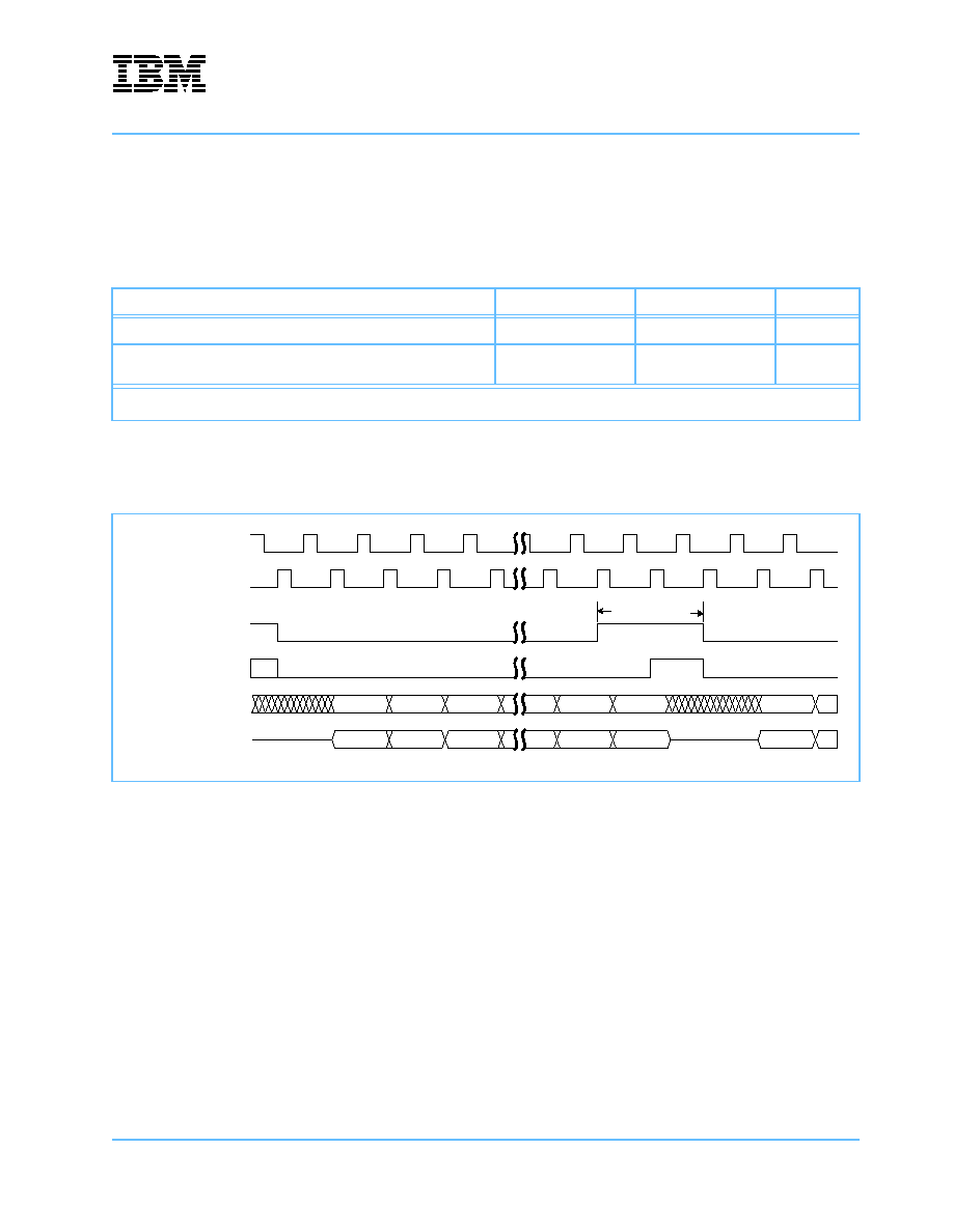
PRS28.4G
IBM Packet Routing Switch
prs28.04.fm
February 6, 2001
I/O Definitions and Timing
Page 105 of 131
7.1 I/O Timing
7.1.1 DASL Signals
The following table provides the skew requirements related to the DASL links.
7.1.2 OCM Interface Signals
Table 24: DASL Interface Skew
Parameter
Rating
Units
Note
Maximum skew between the two lines of a differential pair
� 130
ps
Maximum skew between two 444 Mb/s links of the same port
(This applies also for any two ports in speed expansion)
� 2
clock cycles
1
1. Clock cycle = 9ns (111.1MHz operation) to 10ns (100MHz operation).
Figure 9: OCM Interface Signals Timing Diagram
bit24
bit23
bit22
bit24
bit23
bit22
.....
.....
bit1
bit1
bit0
bit0
LSB
MSB
bit24
bit24
EMB_A_CLK
EMB_B_CLK
NEMB_SELECT
EMB_MODE
EMB_DATA_IN
EMB_DATA_OUT
Pulse > 60 ns

PRS28.4G
IBM Packet Routing Switch
I/O Definitions and Timing
Page 106 of 131
prs28.04.fm
February 6, 2001
7.1.2.1 Timing Window
The sampling window of SND_GRANT(n) is the time window during which the SND_GRANT(n) signal on the
device pin is sampled in order to decide on the transmission of a data or control packet. This window is
defined in relationship with the beginning of transmission of that packet on the chip output pins.
Figure 10: OCM Signal Timing Diagram
Table 25: OCM Signal Timing Values
Symbol
Parameter
Rating
Units
Min.
Max.
t
CYCLE
EMB Clock Cycle Time
16
ns
t
PULSE
EMB Clock Pulse
4
t
NO_LAP
EMB Clock Non Overlap
2
t
IN_SETUP
EMB_Data_In Setup Time
6
t
IN_HOLD
EMB_Data_In Hold Time
0
t
OUT_ARR
EMB_Data_Out Arrival Time
6.5
t
OUT_HOLD
EMB_Data_Out Hold Time
0
t
IN_HOLD
t
IN_SETUP
t
OUT_ARR
t
OUT_HOLD
t
PULSE
t
NO_LAP
t
NO_LAP
EMB_B_CLK
EMB_A_CLK
EMB_DATA_OUT
EMB_DATA_IN
EMB_MODE
nEMB_SELECT
t
CYCLE
t
PULSE
t
PULSE

PRS28.4G
IBM Packet Routing Switch
prs28.04.fm
February 6, 2001
I/O Definitions and Timing
Page 107 of 131
7.1.2.2 RCV_GRANT Sampling Window
The sampling window of RCV_GRANT(n) is the time window during which the RCV_GRANT signals on the
device pins are sampled in order to decide on the reception of a packet for output n. This window is defined in
relationship with the beginning of the packet reception on the chip input pins.
7.1.2.3 Q_FULL, Q_EMPTY and Q_SYNC Bus
(Trb, Tre) and (Tfe, Tfb) defined windows in which the Q_FULL and Q_EMPTY bits will change value for a
new priority, in relation to Q_SYNC rising edge and falling edge respectively.
Figure 11: SND_GRANT(
n
)
Sampling Window in relationship with the packet flow on output
n pins.
Table 26: SND_Grant Sampling Window Timing
Symbol
Parameter
Rating
Note
t
WB
Sampling Window Beginning
(including setup time)
21 ns + 18 byte cycles
1
t
WE
Sampling Window End
(including hold time)
17 ns + 18 byte cycles
1
1. Byte cycle = 9ns (111.1MHz operation) to 10ns (100MHz operation).
Figure 12: RCV_GRANT(
n
)
Sampling Window in relationship with the packet flow on any input.
Table 27: RCV_Grant Sampling Window Timing
Symbol
Parameter
Rating
Note
t
WB
Sampling Window Beginning - (including setup time)
-3 ns + 2 clock cycles
1
t
WE
Sampling Window End -
(including hold time)
14 ns + 5.25 clock cycles
1
1. Clock cycle = 9ns (111.1MHz operation) to 10ns (100MHz operation).
SND_GRANT (n) Sampling Window for packet M
Packet M-1
Packet M
Twe
Twb
Packet Transmission on DASL output pins of port n
RCV_GRANT (n) Sampling Window for packet M
Packet M
Packet M + 1
Twe
Twb
Packet Reception on DASL input pins

PRS28.4G
IBM Packet Routing Switch
I/O Definitions and Timing
Page 108 of 131
prs28.04.fm
February 6, 2001
7.1.3 Master-Slave Speed Expansion Signals
The Master-Slave speed expansion bus (SYS_CLK, MS_SYNC_IN, MS_SYNC_OUT, MS_DASLSYNC_IN,
MS_DASLSYNC_OUT, MS_IN_ADDR, and MS_OUT_ADDR) is synchronous to the internal byte clock of the
devices. They are connected point-to-point between the master and the slave devices. In order to guarantee
the timing on those signals, the wiring is bounded:
Wiring delay on Master-Slave bus: maximum of 1.05 ns, or 15 cm of trace (70 ps/cm for FR4)
Figure 13: Q_FULL, Q_EMPTY, Q_SYNC Timing Diagram
Table 28: Q_FULL, Q_EMPTY, Q_SYNC Timing Values
Symbol
Parameter
Rating
Note
t
CYCLE
Cycle time
NrOfPriorities (1 to 4) x
4 byte cycles
1
t
PULSE
Q_SYNC Pulse
4 byte cycles
1
t
RB
Beginning of Rising Window
0.57ns
t
RE
End of Rising Window
1.05ns
t
FB
Beginning of Falling Window
0.37ns
t
FE
End of Falling Window
1.25ns
1. Byte cycle = 9ns (111.1MHz operation) to 10ns (100MHz operation). Therefore, 4 byte cycles = 36ns (111.1MHz operation) to
40ns (100MHz operation).
t
FE
t
FB
t
RE
t
RB
Q_SYNC
Q_FULL &
t
PULSE
t
CYCLE
(with 4 priorities enabled)
t
PULSE
t
PULSE
t
PULSE

PRS28.4G
IBM Packet Routing Switch
prs28.04.fm
February 6, 2001
Packaging and Pin Information
Page 109 of 131
8. Packaging and Pin Information
Figure 14: Package Physical Dimensions
Ceramic Column Grid Array (CCGA), 32mm x 32mm 624-lead,Dual power supply
AE
AD
AC
AB
AA
0Y
0W
0V
0U
0T
0R
0P
0N
0M
0L
0K
0J
0H
0G
0F
0E
0D
0C
0B
0A
01 02 03 04 05 06 07 08 09 10 11 12 13 14 15 16 17 18 19 20 21 22 23 24 25
30.68 Max
30.28Min
Square
32.48 Max
32.13Min
Square
2.36 Max
2.13 Min
7.51 Max
6.56 Min
87 Mil
1.27
All measurements are millimeters unless otherwise noted

PRS28.4G
IBM Packet Routing Switch
Packaging and Pin Information
Page 110 of 131
prs28.04.fm
February 6, 2001
Table 29: Pin List, Sorted by Pin Name
(Page 1 of 7)
Signal Name
Pin
Signal Name
Pin
Signal Name
Pin
C_CLK_OUTQ
0U05
DATA_IN_03_QN<2>
0H07
DATA_IN_07_QN<2>
0K11
C_CLK_OUTQN
0U03
DATA_IN_03_QN<3>
0B01
DATA_IN_07_QN<3>
0C12
DATA_IN_00_Q<0>
0N05
DATA_IN_04_Q<0>
0A02
DATA_IN_08_Q<0>
0A14
DATA_IN_00_Q<1>
0M02
DATA_IN_04_Q<1>
OE05
DATA_IN_08_Q<1>
0K15
DATA_IN_00_Q<2>
0L10
DATA_IN_04_Q<2>
0E07
DATA_IN_08_Q<2>
0G14
DATA_IN_00_Q<3>
0L02
DATA_IN_04_Q<3>
0H09
DATA_IN_08_Q<3>
0J15
DATA_IN_00_QN<0>
0N04
DATA_IN_04_QN<0>
0B02
DATA_IN_08_QN<0>
0A13
DATA_IN_00_QN<1>
0N02
DATA_IN_04_QN<1>
0D05
DATA_IN_08_QN<1>
0J14
DATA_IN_00_QN<2>
0M09
DATA_IN_04_QN<2>
0E06
DATA_IN_08_QN<2>
0F14
DATA_IN_00_QN<3>
0M01
DATA_IN_04_QN<3>
0G09
DATA_IN_08_QN<3>
0J16
DATA_IN_01_Q<0>
0L06
DATA_IN_05_Q<0>
0A05
DATA_IN_09_Q<0>
0E14
DATA_IN_01_Q<1>
0K02
DATA_IN_05_Q<1>
0D08
DATA_IN_09_Q<1>
0G15
DATA_IN_01_Q<2>
0K03
DATA_IN_05_Q<2>
0F09
DATA_IN_09_Q<2>
0D16
DATA_IN_01_Q<3>
0L04
DATA_IN_05_Q<3>
0B08
DATA_IN_09_Q<3>
0B17
DATA_IN_01_QN<0>
0L07
DATA_IN_05_QN<0>
0A06
DATA_IN_09_QN<0>
0D15
DATA_IN_01_QN<1>
0K01
DATA_IN_05_QN<1>
0E08
DATA_IN_09_QN<1>
0F15
DATA_IN_01_QN<2>
0J02
DATA_IN_05_QN<2>
0G10
DATA_IN_09_QN<2>
0C16
DATA_IN_01_QN<3>
0K05
DATA_IN_05_QN<3>
0B07
DATA_IN_09_QN<3>
0D17
DATA_IN_02_Q<0>
0H03
DATA_IN_06_Q<0>
0B09
DATA_IN_10_Q<0>
0B18
DATA_IN_02_Q<1>
0J06
DATA_IN_06_Q<1>
0C10
DATA_IN_10_Q<1>
0G16
DATA_IN_02_Q<2>
0F01
DATA_IN_06_Q<2>
0F11
DATA_IN_10_Q<2>
OE18
DATA_IN_02_Q<3>
0D01
DATA_IN_06_Q<3>
0B11
DATA_IN_10_Q<3>
0H17
DATA_IN_02_QN<0>
0J04
DATA_IN_06_QN<0>
0A08
DATA_IN_10_QN<0>
0A18
DATA_IN_02_QN<1>
0K07
DATA_IN_06_QN<1>
0D10
DATA_IN_10_QN<1>
0F17
DATA_IN_02_QN<2>
0E02
DATA_IN_06_QN<2>
0G11
DATA_IN_10_QN<2>
0D18
DATA_IN_02_QN<3>
0E01
DATA_IN_06_QN<3>
0D11
DATA_IN_10_QN<3>
0G17
DATA_IN_03_Q<0>
0C01
DATA_IN_07_Q<0>
0J10
DATA_IN_11_Q<0>
0E20
DATA_IN_03_Q<1>
0E03
DATA_IN_07_Q<1>
0F12
DATA_IN_11_Q<1>
0C21
DATA_IN_03_Q<2>
0G06
DATA_IN_07_Q<2>
0J12
DATA_IN_11_Q<2>
0C23
DATA_IN_03_Q<3>
0C02
DATA_IN_07_Q<3>
0B13
DATA_IN_11_Q<3>
0B24
DATA_IN_03_QN<0>
0D02
DATA_IN_07_QN<0>
0J11
DATA_IN_11_QN<0>
0C20
DATA_IN_03_QN<1>
0E04
DATA_IN_07_QN<1>
0G12
DATA_IN_11_QN<1>
0D21

PRS28.4G
IBM Packet Routing Switch
prs28.04.fm
February 6, 2001
Packaging and Pin Information
Page 111 of 131
DATA_IN_11_QN<2>
0C22
DATA_IN_15_QN<2>
0M15
DATA_OUT_03_QN<2>
AC25
DATA_IN_11_QN<3>
0A24
DATA_IN_15_QN<3>
0N18
DATA_OUT_03_QN<3>
AB24
DATA_IN_12_Q<0>
0F21
DATA_OUT_00_Q<0>
0N21
DATA_OUT_04_Q<0>
AD23
DATA_IN_12_Q<1>
0G20
DATA_OUT_00_Q<1>
0N16
DATA_OUT_04_Q<1>
AE22
DATA_IN_12_Q<2>
0E23
DATA_OUT_00_Q<2>
0P15
DATA_OUT_04_Q<2>
AC21
DATA_IN_12_Q<3>
0D24
DATA_OUT_00_Q<3>
0R16
DATA_OUT_04_Q<3>
AE21
DATA_IN_12_QN<0>
0F20
DATA_OUT_00_QN<0>
0N22
DATA_OUT_04_QN<0>
AC23
DATA_IN_12_QN<1>
0G19
DATA_OUT_00_QN<1>
0N17
DATA_OUT_04_QN<1>
AE23
DATA_IN_12_QN<2>
0D23
DATA_OUT_00_QN<2>
0P17
DATA_OUT_04_QN<2>
AB21
DATA_IN_12_QN<3>
0C25
DATA_OUT_00_QN<3>
0R17
DATA_OUT_04_QN<3>
AD21
DATA_IN_13_Q<0>
0J18
DATA_OUT_01_Q<0>
0P25
DATA_OUT_05_Q<0>
AB19
DATA_IN_13_Q<1>
0H19
DATA_OUT_01_Q<1>
0R24
DATA_OUT_05_Q<1>
AC18
DATA_IN_13_Q<2>
OE25
DATA_OUT_01_Q<2>
0R19
DATA_OUT_05_Q<2>
AD17
DATA_IN_13_Q<3>
0H22
DATA_OUT_01_Q<3>
0T25
DATA_OUT_05_Q<3>
AC16
DATA_IN_13_QN<0>
0J19
DATA_OUT_01_QN<0>
0P24
DATA_OUT_05_QN<0>
AC20
DATA_IN_13_QN<1>
0H20
DATA_OUT_01_QN<1>
0R22
DATA_OUT_05_QN<1>
AD19
DATA_IN_13_QN<2>
0D25
DATA_OUT_01_QN<2>
0R20
DATA_OUT_05_QN<2>
AB17
DATA_IN_13_QN<3>
0G22
DATA_OUT_01_QN<3>
0T24
DATA_OUT_05_QN<3>
AB16
DATA_IN_14_Q<0>
0K19
DATA_OUT_02_Q<0>
0T21
DATA_OUT_06_Q<0>
0V15
DATA_IN_14_Q<1>
0K25
DATA_OUT_02_Q<1>
0U22
DATA_OUT_06_Q<1>
AD15
DATA_IN_14_Q<2>
0L19
DATA_OUT_02_Q<2>
0W22
DATA_OUT_06_Q<2>
0U15
DATA_IN_14_Q<3>
0K17
DATA_OUT_02_Q<3>
0U18
DATA_OUT_06_Q<3>
AC14
DATA_IN_14_QN<0>
0J20
DATA_OUT_02_QN<0>
0T23
DATA_OUT_06_QN<0>
0U16
DATA_IN_14_QN<1>
0K24
DATA_OUT_02_QN<1>
0U20
DATA_OUT_06_QN<1>
AB15
DATA_IN_14_QN<2>
0L20
DATA_OUT_02_QN<2>
0W24
DATA_OUT_06_QN<2>
0T15
DATA_IN_14_QN<3>
0L17
DATA_OUT_02_QN<3>
0U19
DATA_OUT_06_QN<3>
AA14
DATA_IN_15_Q<0>
0M24
DATA_OUT_03_Q<0>
AA25
DATA_OUT_07_Q<0>
0W14
DATA_IN_15_Q<1>
0M19
DATA_OUT_03_Q<1>
0W20
DATA_OUT_07_Q<1>
AE13
DATA_IN_15_Q<2>
0L16
DATA_OUT_03_Q<2>
AB25
DATA_OUT_07_Q<2>
0U13
DATA_IN_15_Q<3>
0N20
DATA_OUT_03_Q<3>
AB23
DATA_OUT_07_Q<3>
AA13
DATA_IN_15_QN<0>
0L24
DATA_OUT_03_QN<0>
AA23
DATA_OUT_07_QN<0>
0U14
DATA_IN_15_QN<1>
0M17
DATA_OUT_03_QN<1>
0W21
DATA_OUT_07_QN<1>
AC13
Table 29: Pin List, Sorted by Pin Name
(Page 2 of 7)
Signal Name
Pin
Signal Name
Pin
Signal Name
Pin

PRS28.4G
IBM Packet Routing Switch
Packaging and Pin Information
Page 112 of 131
prs28.04.fm
February 6, 2001
DATA_OUT_07_QN<2>
0T13
DATA_OUT_11_QN<2>
AB05
DATA_OUT_15_QN<2>
0R09
DATA_OUT_07_QN<3>
0Y13
DATA_OUT_11_QN<3>
AE02
DATA_OUT_15_QN<3>
0R10
DATA_OUT_08_Q<0>
AC12
DATA_OUT_12_Q<0>
0Y05
DBG_DATA<0>
OE13
DATA_OUT_08_Q<1>
0T11
DATA_OUT_12_Q<1>
AA03
DBG_DATA<10>
0C05
DATA_OUT_08_Q<2>
0W12
DATA_OUT_12_Q<2>
AA02
DBG_DATA<11>
0B05
DATA_OUT_08_Q<3>
0U11
DATA_OUT_12_Q<3>
0V07
DBG_DATA<12>
0C04
DATA_OUT_08_QN<0>
AD13
DATA_OUT_12_QN<0>
AA05
DBG_DATA<13>
0A04
DATA_OUT_08_QN<1>
0U12
DATA_OUT_12_QN<1>
AB03
DBG_DATA<14>
0B03
DATA_OUT_08_QN<2>
AA12
DATA_OUT_12_QN<2>
AB02
DBG_DATA<15>
0A03
DATA_OUT_08_QN<3>
0U10
DATA_OUT_12_QN<3>
0V06
DBG_DATA<1>
0D13
DATA_OUT_09_Q<0>
0V11
DATA_OUT_13_Q<0>
AA01
DBG_DATA<2>
OE12
DATA_OUT_09_Q<1>
AB10
DATA_OUT_13_Q<1>
0W02
DBG_DATA<3>
0A12
DATA_OUT_09_Q<2>
AD09
DATA_OUT_13_Q<2>
0V04
DBG_DATA<4>
OE10
DATA_OUT_09_Q<3>
AD08
DATA_OUT_13_Q<3>
0U06
DBG_DATA<5>
0A10
DATA_OUT_09_QN<0>
0W11
DATA_OUT_13_QN<0>
0Y01
DBG_DATA<6>
0D09
DATA_OUT_09_QN<1>
AC10
DATA_OUT_13_QN<1>
0W04
DBG_DATA<7>
0C08
DATA_OUT_09_QN<2>
AB09
DATA_OUT_13_QN<2>
0V05
DBG_DATA<8>
0D07
DATA_OUT_09_QN<3>
AE08
DATA_OUT_13_QN<3>
0T07
DBG_DATA<9>
0C06
DATA_OUT_10_Q<0>
AB07
DATA_OUT_14_Q<0>
0T03
DBG_SELECT<0>
0G04
DATA_OUT_10_Q<1>
AA08
DATA_OUT_14_Q<1>
0R07
DBG_SELECT<1>
0G07
DATA_OUT_10_Q<2>
AD05
DATA_OUT_14_Q<2>
0T01
DBG_SELECT<2>
0F03
DATA_OUT_10_Q<3>
0V09
DATA_OUT_14_Q<3>
0R06
DBG_SELECT<3>
0F05
DATA_OUT_10_QN<0>
AC08
DATA_OUT_14_QN<0>
0U04
DBG_SELECT<4>
0D03
DATA_OUT_10_QN<1>
AB08
DATA_OUT_14_QN<1>
0R08
DBG_SELECT<5>
0G08
DATA_OUT_10_QN<2>
AE05
DATA_OUT_14_QN<2>
0T02
DBG_SELECT<6>
0F07
DATA_OUT_10_QN<3>
0W09
DATA_OUT_14_QN<3>
0R04
DBG_SELECT<7>
0C03
DATA_OUT_11_Q<0>
AA06
DATA_OUT_15_Q<0>
0P01
DELAY_OUT
AA11
DATA_OUT_11_Q<1>
AC04
DATA_OUT_15_Q<1>
0U09
EMB_A_CLK
AC07
DATA_OUT_11_Q<2>
AC05
DATA_OUT_15_Q<2>
0P09
EMB_B_CLK
AE07
DATA_OUT_11_Q<3>
AD02
DATA_OUT_15_Q<3>
0P11
EMB_DATA_IN
AD01
DATA_OUT_11_QN<0>
AC06
DATA_OUT_15_QN<0>
0P02
EMB_DATA_OUT
AE03
DATA_OUT_11_QN<1>
AD03
DATA_OUT_15_QN<1>
0T09
EMB_MODE
AE04
Table 29: Pin List, Sorted by Pin Name
(Page 3 of 7)
Signal Name
Pin
Signal Name
Pin
Signal Name
Pin

PRS28.4G
IBM Packet Routing Switch
prs28.04.fm
February 6, 2001
Packaging and Pin Information
Page 113 of 131
IOTEST
0C11
MS_OUT_ADDR<1>
0V19
Q_EMPTY<6>
AE16
LSSD_A_CLK
0J03
MS_OUT_ADDR<2>
0W19
Q_EMPTY<7>
0W15
LSSD_B2_CLK
OE11
MS_OUT_ADDR<3>
AA24
Q_EMPTY<8>
0R14
LSSD_B_CLK
0J05
MS_OUT_ADDR<4>
AA22
Q_EMPTY<9>
AE14
LSSD_C1_CLK
0L01
MS_OUT_ADDR<5>
AA20
Q_FULL<0>
0Y11
LSSD_C2_CLK
0L03
MS_OUT_ADDR<6>
AA19
Q_FULL<10>
0Y06
LSSD_C3_CLK
OE09
MS_OUT_ADDR<7>
AA18
Q_FULL<11>
AC02
LSSD_SCAN_GATE
0L05
MS_OUT_ADDR<8>
AC22
Q_FULL<12>
AA04
LSSD_SCAN_MODE
0G01
MS_OUT_ADDR<9>
AD24
Q_FULL<13>
0U08
LSSD_TAP_C1
0G03
MS_SYNC_IN
0R18
Q_FULL<14>
AB01
LSSD_TAP_C2
0J01
MS_SYNC_OUT
0N24
Q_FULL<15>
0Y03
MEM_GRANT<0>
0B25
NDI1
AE09
Q_FULL<1>
AB11
MEM_GRANT<1>
0C24
NDI2
AC11
Q_FULL<2>
AD11
MEM_GRANT<2>
0B23
NEMB_SELECT
AD07
Q_FULL<3>
0W10
MEM_GRANT<3>
0A23
NEMB_SIGOUT
AC01
Q_FULL<4>
AA10
MS_DASLSYNC_IN<0>
0G24
NRESET
AA09
Q_FULL<5>
AE10
MS_DASLSYNC_IN<1>
0F25
PLL_LOCK
0R01
Q_FULL<6>
0Y09
MS_DASLSYNC_OUT<0>
0M23
PLL_TESTIN
0R05
Q_FULL<7>
AA07
MS_DASLSYNC_OUT<1>
0L22
PLL_TESTOUT
0U01
Q_FULL<8>
0W08
MS_IN_ADDR<0>
0M21
PLL_VDDA
0R03
Q_FULL<9>
0Y07
MS_IN_ADDR<10>
0V21
Q_EMPTY<0>
0L12
Q_FULL_SYNC
AE12
MS_IN_ADDR<1>
0N23
Q_EMPTY<10>
0P13
RAM_BURN_IN
AC09
MS_IN_ADDR<2>
0P23
Q_EMPTY<11>
0N12
RCV_GRANT<0>
0M07
MS_IN_ADDR<3>
0P21
Q_EMPTY<12>
0W13
RCV_GRANT<10>
0U02
MS_IN_ADDR<4>
0P19
Q_EMPTY<13>
0M11
RCV_GRANT<11>
0V03
MS_IN_ADDR<5>
0T19
Q_EMPTY<14>
0R12
RCV_GRANT<12>
0V01
MS_IN_ADDR<6>
0U24
Q_EMPTY<15>
0Y12
RCV_GRANT<13>
0W07
MS_IN_ADDR<7>
0V25
Q_EMPTY<1>
0V17
RCV_GRANT<14>
0W06
MS_IN_ADDR<8>
0V23
Q_EMPTY<2>
AB18
RCV_GRANT<15>
0W05
MS_IN_ADDR<9>
0V22
Q_EMPTY<3>
AE18
RCV_GRANT<1>
0M05
MS_OUT_ADDR<0>
0V20
Q_EMPTY<4>
AD18
RCV_GRANT<2>
0M03
MS_OUT_ADDR<10>
AE20
Q_EMPTY<5>
0U17
RCV_GRANT<3>
0N07
Table 29: Pin List, Sorted by Pin Name
(Page 4 of 7)
Signal Name
Pin
Signal Name
Pin
Signal Name
Pin

PRS28.4G
IBM Packet Routing Switch
Packaging and Pin Information
Page 114 of 131
prs28.04.fm
February 6, 2001
RCV_GRANT<4>
0N01
SCAN_OUT<6>
AE19
VREF_MS_SYNC
0J24
RCV_GRANT<5>
0P07
SCAN_OUT<7>
AC19
WTEST
0R25
RCV_GRANT<6>
0P03
SCAN_OUT<8>
0U21
VDD
0D04
RCV_GRANT<7>
0R02
SCAN_OUT<9>
0R21
VDD
0D12
RCV_GRANT<8>
0T05
SEQ_CLK
0N25
VDD
0D14
RCV_GRANT<9>
0U07
SEQ_CLK_TTL
0N14
VDD
0D22
SCAN_IN<0>
0A15
SIDD
AE11
VDD
0H08
SCAN_IN<10>
0G23
SND_GRANT<0>
0F23
VDD
0H12
SCAN_IN<11>
0J23
SND_GRANT<10>
0B19
VDD
0H14
SCAN_IN<12>
0L23
SND_GRANT<11>
0G18
VDD
0H18
SCAN_IN<13>
0G25
SND_GRANT<12>
0C18
VDD
0L11
SCAN_IN<14>
0J25
SND_GRANT<13>
OE16
VDD
0L15
SCAN_IN<1>
0C15
SND_GRANT<14>
0A16
VDD
0M04
SCAN_IN<2>
OE15
SND_GRANT<15>
0B15
VDD
0M08
SCAN_IN<3>
0A17
SND_GRANT<1>
OE22
VDD
0M12
SCAN_IN<4>
0C17
SND_GRANT<2>
0A22
VDD
0M14
SCAN_IN<5>
OE17
SND_GRANT<3>
0G21
VDD
0M18
SCAN_IN<6>
0A19
SND_GRANT<4>
0B21
VDD
0M22
SCAN_IN<7>
0C19
SND_GRANT<5>
0A21
VDD
0P04
SCAN_IN<8>
0J21
SND_GRANT<6>
0A20
VDD
0P08
SCAN_IN<9>
0L21
SND_GRANT<7>
0F19
VDD
0P12
SCAN_OUT<0>
AE15
SND_GRANT<8>
OE19
VDD
0P14
SCAN_OUT<10>
0W23
SND_GRANT<9>
0D19
VDD
0P18
SCAN_OUT<11>
0U23
SYS_CLKQ
0W03
VDD
0P22
SCAN_OUT<12>
0R23
SYS_CLKQN
0W01
VDD
0R11
SCAN_OUT<13>
0W25
TCK
0C07
VDD
0R15
SCAN_OUT<14>
0U25
TDI
0A09
VDD
0V08
SCAN_OUT<1>
AC15
TDO
0A11
VDD
0V12
SCAN_OUT<2>
AA15
TMS
0A07
VDD
0V14
SCAN_OUT<3>
AE17
TRST
0C09
VDD
0V18
SCAN_OUT<4>
AC17
VREF_MS_IN
0M13
VDD
AB04
SCAN_OUT<5>
AA17
VREF_MS_OUT
0W18
VDD
AB12
Table 29: Pin List, Sorted by Pin Name
(Page 5 of 7)
Signal Name
Pin
Signal Name
Pin
Signal Name
Pin

PRS28.4G
IBM Packet Routing Switch
prs28.04.fm
February 6, 2001
Packaging and Pin Information
Page 115 of 131
VDD
AB14
VDR
0L25
GND
0J07
VDD
AB22
VDR
0N03
GND
0J08
VDD2
0B06
VDR
0N19
GND
0J09
VDD2
0B10
VDR
0V13
GND
0J13
VDD2
0B16
GND
0A25
GND
0J17
VDD2
0B20
GND
0B04
GND
0J22
VDD2
0F02
GND
0B12
GND
0K04
VDD2
0F10
GND
0B14
GND
0K08
VDD2
0F16
GND
0B22
GND
0K09
VDD2
0F24
GND
0C13
GND
0K12
VDD2
0K06
GND
0C14
GND
0K13
VDD2
0K10
GND
0D06
GND
0K14
VDD2
0K16
GND
0D20
GND
0K18
VDD2
0K20
GND
0F04
GND
0K21
VDD2
0L13
GND
0F08
GND
0K22
VDD2
0N11
GND
0F13
GND
0K23
VDD2
0N13
GND
0F18
GND
0L08
VDD2
0N15
GND
0F22
GND
0L09
VDD2
0R13
GND
0G02
GND
0L14
VDD2
0T06
GND
0G13
GND
0L18
VDD2
0T10
GND
0H02
GND
0M06
VDD2
0T16
GND
0H04
GND
0M10
VDD2
0T20
GND
0H05
GND
0M16
VDD2
0Y02
GND
0H06
GND
0M20
VDD2
0Y10
GND
0H10
GND
0N08
VDD2
0Y16
GND
0H11
GND
0N10
VDD2
0Y24
GND
0H15
GND
0P06
VDD2
AD06
GND
0H16
GND
0P10
VDD2
AD10
GND
0H21
GND
0P16
VDD2
AD16
GND
0H23
GND
0P20
VDD2
AD20
GND
0H24
GND
0T04
VDR
0H13
GND
0H25
GND
0T08
Table 29: Pin List, Sorted by Pin Name
(Page 6 of 7)
Signal Name
Pin
Signal Name
Pin
Signal Name
Pin

PRS28.4G
IBM Packet Routing Switch
Packaging and Pin Information
Page 116 of 131
prs28.04.fm
February 6, 2001
GND
0T12
N.C.
0N06
GND
0T14
N.C.
0N09
GND
0T17
N.C.
0P05
GND
0T18
N.C.
0Y14
GND
0T22
N.C.
0Y15
GND
0V02
N.C.
0Y17
GND
0V10
N.C.
0Y19
GND
0V16
N.C.
0Y20
GND
0V24
N.C.
0Y21
GND
0W16
N.C.
0Y23
GND
0W17
N.C.
0Y25
GND
0Y04
N.C.
AA21
GND
0Y08
N.C.
AB13
GND
0Y18
N.C.
AC03
GND
0Y22
N.C.
AD25
GND
AA16
N.C.
AE06
GND
AB06
GND
AB20
GND
AC24
GND
AD04
GND
AD12
GND
AD14
GND
AD22
GND
AE01
GND
AE24
GND
AE25
N.C.
OE21
N.C.
OE24
N.C.
0F06
N.C.
0G05
N.C.
0H01
N.C.
0M25
Table 29: Pin List, Sorted by Pin Name
(Page 7 of 7)
Signal Name
Pin
Signal Name
Pin
Signal Name
Pin

PRS28.4G
IBM Packet Routing Switch
prs28.04.fm
February 6, 2001
Packaging and Pin Information
Page 117 of 131
Table 30: Pin List, Sorted by Pin Number
(Page 1 of 7)
Pin
Signal Name
Pin
Signal Name
Pin
Signal Name
0A02
DATA_IN_04_Q<0>
0B09
DATA_IN_06_Q<0>
0C16
DATA_IN_09_QN<2>
0A03
DBG_DATA<15>
0B10
VDD2
0C17
SCAN_IN<4>
0A04
DBG_DATA<13>
0B11
DATA_IN_06_Q<3>
0C18
SND_GRANT<12>
0A05
DATA_IN_05_Q<0>
0B12
GND
0C19
SCAN_IN<7>
0A06
DATA_IN_05_QN<0>
0B13
DATA_IN_07_Q<3>
0C20
DATA_IN_11_QN<0>
0A07
TMS
0B14
GND
0C21
DATA_IN_11_Q<1>
0A08
DATA_IN_06_QN<0>
0B15
SND_GRANT<15>
0C22
DATA_IN_11_QN<2>
0A09
TDI
0B16
VDD2
0C23
DATA_IN_11_Q<2>
0A10
DBG_DATA<5>
0B17
DATA_IN_09_Q<3>
0C24
MEM_GRANT<1>
0A11
TDO
0B18
DATA_IN_10_Q<0>
0C25
DATA_IN_12_QN<3>
0A12
DBG_DATA<3>
0B19
SND_GRANT<10>
0D01
DATA_IN_02_Q<3>
0A13
DATA_IN_08_QN<0>
0B20
VDD2
0D02
DATA_IN_03_QN<0>
0A14
DATA_IN_08_Q<0>
0B21
SND_GRANT<4>
0D03
DBG_SELECT<4>
0A15
SCAN_IN<0>
0B22
GND
0D04
VDD
0A16
SND_GRANT<14>
0B23
MEM_GRANT<2>
0D05
DATA_IN_04_QN<1>
0A17
SCAN_IN<3>
0B24
DATA_IN_11_Q<3>
0D06
GND
0A18
DATA_IN_10_QN<0>
0B25
MEM_GRANT<0>
0D07
DBG_DATA<8>
0A19
SCAN_IN<6>
0C01
DATA_IN_03_Q<0>
0D08
DATA_IN_05_Q<1>
0A20
SND_GRANT<6>
0C02
DATA_IN_03_Q<3>
0D09
DBG_DATA<6>
0A21
SND_GRANT<5>
0C03
DBG_SELECT<7>
0D10
DATA_IN_06_QN<1>
0A22
SND_GRANT<2>
0C04
DBG_DATA<12>
0D11
DATA_IN_06_QN<3>
0A23
MEM_GRANT<3>
0C05
DBG_DATA<10>
0D12
VDD
0A24
DATA_IN_11_QN<3>
0C06
DBG_DATA<9>
0D13
DBG_DATA<1>
0A25
GND
0C07
TCK
0D14
VDD
0B01
DATA_IN_03_QN<3>
0C08
DBG_DATA<7>
0D15
DATA_IN_09_QN<0>
0B02
DATA_IN_04_QN<0>
0C09
TRST
0D16
DATA_IN_09_Q<2>
0B03
DBG_DATA<14>
0C10
DATA_IN_06_Q<1>
0D17
DATA_IN_09_QN<3>
0B04
GND
0C11
IOTEST
0D18
DATA_IN_10_QN<2>
0B05
DBG_DATA<11>
0C12
DATA_IN_07_QN<3>
0D19
SND_GRANT<9>
0B06
VDD2
0C13
GND
0D20
GND
0B07
DATA_IN_05_QN<3>
0C14
GND
0D21
DATA_IN_11_QN<1>
0B08
DATA_IN_05_Q<3>
0C15
SCAN_IN<1>
0D22
VDD

PRS28.4G
IBM Packet Routing Switch
Packaging and Pin Information
Page 118 of 131
prs28.04.fm
February 6, 2001
0D23
DATA_IN_12_QN<2>
0F05
DBG_SELECT<3>
0G12
DATA_IN_07_QN<1>
0D24
DATA_IN_12_Q<3>
0F06
N.C.
0G13
GND
0D25
DATA_IN_13_QN<2>
0F07
DBG_SELECT<6>
0G14
DATA_IN_08_Q<2>
OE01
DATA_IN_02_QN<3>
0F08
GND
0G15
DATA_IN_09_Q<1>
OE02
DATA_IN_02_QN<2>
0F09
DATA_IN_05_Q<2>
0G16
DATA_IN_10_Q<1>
OE03
DATA_IN_03_Q<1>
0F10
VDD2
0G17
DATA_IN_10_QN<3>
OE04
DATA_IN_03_QN<1>
0F11
DATA_IN_06_Q<2>
0G18
SND_GRANT<11>
OE05
DATA_IN_04_Q<1>
0F12
DATA_IN_07_Q<1>
0G19
DATA_IN_12_QN<1>
OE06
DATA_IN_04_QN<2>
0F13
GND
0G20
DATA_IN_12_Q<1>
OE07
DATA_IN_04_Q<2>
0F14
DATA_IN_08_QN<2>
0G21
SND_GRANT<3>
OE08
DATA_IN_05_QN<1>
0F15
DATA_IN_09_QN<1>
0G22
DATA_IN_13_QN<3>
OE09
LSSD_C3_CLK
0F16
VDD2
0G23
SCAN_IN<10>
OE10
DBG_DATA<4>
0F17
DATA_IN_10_QN<1>
0G24
MS_DASLSYNC_IN<0>
OE11
LSSD_B2_CLK
0F18
GND
0G25
SCAN_IN<13>
OE12
DBG_DATA<2>
0F19
SND_GRANT<7>
0H01
N.C.
OE13
DBG_DATA<0>
0F20
DATA_IN_12_QN<0>
0H02
GND
OE14
DATA_IN_09_Q<0>
0F21
DATA_IN_12_Q<0>
0H03
DATA_IN_02_Q<0>
OE15
SCAN_IN<2>
0F22
GND
0H04
GND
OE16
SND_GRANT<13>
0F23
SND_GRANT<0>
0H05
GND
OE17
SCAN_IN<5>
0F24
VDD2
0H06
GND
OE18
DATA_IN_10_Q<2>
0F25
MS_DASLSYNC_IN<1>
0H07
DATA_IN_03_QN<2>
OE19
SND_GRANT<8>
0G01
LSSD_SCAN_MODE
0H08
VDD
OE20
DATA_IN_11_Q<0>
0G02
GND
0H09
DATA_IN_04_Q<3>
OE21
N.C.
0G03
LSSD_TAP_C1
0H10
GND
OE22
SND_GRANT<1>
0G04
DBG_SELECT<0>
0H11
GND
OE23
DATA_IN_12_Q<2>
0G05
N.C.
0H12
VDD
OE24
N.C.
0G06
DATA_IN_03_Q<2>
0H13
VDR
OE25
DATA_IN_13_Q<2>
0G07
DBG_SELECT<1>
0H14
VDD
0F01
DATA_IN_02_Q<2>
0G08
DBG_SELECT<5>
0H15
GND
0F02
VDD2
0G09
DATA_IN_04_QN<3>
0H16
GND
0F03
DBG_SELECT<2>
0G10
DATA_IN_05_QN<2>
0H17
DATA_IN_10_Q<3>
0F04
GND
0G11
DATA_IN_06_QN<2>
0H18
VDD
Table 30: Pin List, Sorted by Pin Number
(Page 2 of 7)
Pin
Signal Name
Pin
Signal Name
Pin
Signal Name

PRS28.4G
IBM Packet Routing Switch
prs28.04.fm
February 6, 2001
Packaging and Pin Information
Page 119 of 131
0H19
DATA_IN_13_Q<1>
0K01
DATA_IN_01_QN<1>
0L08
GND
0H20
DATA_IN_13_QN<1>
0K02
DATA_IN_01_Q<1>
0L09
GND
0H21
GND
0K03
DATA_IN_01_Q<2>
0L10
DATA_IN_00_Q<2>
0H22
DATA_IN_13_Q<3>
0K04
GND
0L11
VDD
0H23
GND
0K05
DATA_IN_01_QN<3>
0L12
Q_EMPTY<0>
0H24
GND
0K06
VDD2
0L13
VDD2
0H25
GND
0K07
DATA_IN_02_QN<1>
0L14
GND
0J01
LSSD_TAP_C2
0K08
GND
0L15
VDD
0J02
DATA_IN_01_QN<2>
0K09
GND
0L16
DATA_IN_15_Q<2>
0J03
LSSD_A_CLK
0K10
VDD2
0L17
DATA_IN_14_QN<3>
0J04
DATA_IN_02_QN<0>
0K11
DATA_IN_07_QN<2>
0L18
GND
0J05
LSSD_B_CLK
0K12
GND
0L19
DATA_IN_14_Q<2>
0J06
DATA_IN_02_Q<1>
0K13
GND
0L20
DATA_IN_14_QN<2>
0J07
GND
0K14
GND
0L21
SCAN_IN<9>
0J08
GND
0K15
DATA_IN_08_Q<1>
0L22
MS_DASLSYNC_OUT<1>
0J09
GND
0K16
VDD2
0L23
SCAN_IN<12>
0J10
DATA_IN_07_Q<0>
0K17
DATA_IN_14_Q<3>
0L24
DATA_IN_15_QN<0>
0J11
DATA_IN_07_QN<0>
0K18
GND
0L25
VDR
0J12
DATA_IN_07_Q<2>
0K19
DATA_IN_14_Q<0>
0M01
DATA_IN_00_QN<3>
0J13
GND
0K20
VDD2
0M02
DATA_IN_00_Q<1>
0J14
DATA_IN_08_QN<1>
0K21
GND
0M03
RCV_GRANT<2>
0J15
DATA_IN_08_Q<3>
0K22
GND
0M04
VDD
0J16
DATA_IN_08_QN<3>
0K23
GND
0M05
RCV_GRANT<1>
0J17
GND
0K24
DATA_IN_14_QN<1>
0M06
GND
0J18
DATA_IN_13_Q<0>
0K25
DATA_IN_14_Q<1>
0M07
RCV_GRANT<0>
0J19
DATA_IN_13_QN<0>
0L01
LSSD_C1_CLK
0M08
VDD
0J20
DATA_IN_14_QN<0>
0L02
DATA_IN_00_Q<3>
0M09
DATA_IN_00_QN<2>
0J21
SCAN_IN<8>
0L03
LSSD_C2_CLK
0M10
GND
0J22
GND
0L04
DATA_IN_01_Q<3>
0M11
Q_EMPTY<13>
0J23
SCAN_IN<11>
0L05
LSSD_SCAN_GATE
0M12
VDD
0J24
VREF_MS_SYNC
0L06
DATA_IN_01_Q<0>
0M13
VREF_MS_IN
0J25
SCAN_IN<14>
0L07
DATA_IN_01_QN<0>
0M14
VDD
Table 30: Pin List, Sorted by Pin Number
(Page 3 of 7)
Pin
Signal Name
Pin
Signal Name
Pin
Signal Name

PRS28.4G
IBM Packet Routing Switch
Packaging and Pin Information
Page 120 of 131
prs28.04.fm
February 6, 2001
0M15
DATA_IN_15_QN<2>
0N22
DATA_OUT_00_QN<0>
0R04
DATA_OUT_14_QN<3>
0M16
GND
0N23
MS_IN_ADDR<1>
0R05
PLL_TESTIN
0M17
DATA_IN_15_QN<1>
0N24
MS_SYNC_OUT
0R06
DATA_OUT_14_Q<3>
0M18
VDD
0N25
SEQ_CLK
0R07
DATA_OUT_14_Q<1>
0M19
DATA_IN_15_Q<1>
0P01
DATA_OUT_15_Q<0>
0R08
DATA_OUT_14_QN<1>
0M20
GND
0P02
DATA_OUT_15_QN<0>
0R09
DATA_OUT_15_QN<2>
0M21
MS_IN_ADDR<0>
0P03
RCV_GRANT<6>
0R10
DATA_OUT_15_QN<3>
0M22
VDD
0P04
VDD
0R11
VDD
0M23
MS_DASLSYNC_OUT<0>
0P05
N.C.
0R12
Q_EMPTY<14>
0M24
DATA_IN_15_Q<0>
0P06
GND
0R13
VDD2
0M25
N.C.
0P07
RCV_GRANT<5>
0R14
Q_EMPTY<8>
0N01
RCV_GRANT<4>
0P08
VDD
0R15
VDD
0N02
DATA_IN_00_QN<1>
0P09
DATA_OUT_15_Q<2>
0R16
DATA_OUT_00_Q<3>
0N03
VDR
0P10
GND
0R17
DATA_OUT_00_QN<3>
0N04
DATA_IN_00_QN<0>
0P11
DATA_OUT_15_Q<3>
0R18
MS_SYNC_IN
0N05
DATA_IN_00_Q<0>
0P12
VDD
0R19
DATA_OUT_01_Q<2>
0N06
N.C.
0P13
Q_EMPTY<10>
0R20
DATA_OUT_01_QN<2>
0N07
RCV_GRANT<3>
0P14
VDD
0R21
SCAN_OUT<9>
0N08
GND
0P15
DATA_OUT_00_Q<2>
0R22
DATA_OUT_01_QN<1>
0N09
N.C.
0P16
GND
0R23
SCAN_OUT<12>
0N10
GND
0P17
DATA_OUT_00_QN<2>
0R24
DATA_OUT_01_Q<1>
0N11
VDD2
0P18
VDD
0R25
WTEST
0N12
Q_EMPTY<11>
0P19
MS_IN_ADDR<4>
0T01
DATA_OUT_14_Q<2>
0N13
VDD2
0P20
GND
0T02
DATA_OUT_14_QN<2>
0N14
SEQ_CLK_TTL
0P21
MS_IN_ADDR<3>
0T03
DATA_OUT_14_Q<0>
0N15
VDD2
0P22
VDD
0T04
GND
0N16
DATA_OUT_00_Q<1>
0P23
MS_IN_ADDR<2>
0T05
RCV_GRANT<8>
0N17
DATA_OUT_00_QN<1>
0P24
DATA_OUT_01_QN<0>
0T06
VDD2
0N18
DATA_IN_15_QN<3>
0P25
DATA_OUT_01_Q<0>
0T07
DATA_OUT_13_QN<3>
0N19
VDR
0R01
PLL_LOCK
0T08
GND
0N20
DATA_IN_15_Q<3>
0R02
RCV_GRANT<7>
0T09
DATA_OUT_15_QN<1>
0N21
DATA_OUT_00_Q<0>
0R03
PLL_VDDA
0T10
VDD2
Table 30: Pin List, Sorted by Pin Number
(Page 4 of 7)
Pin
Signal Name
Pin
Signal Name
Pin
Signal Name

PRS28.4G
IBM Packet Routing Switch
prs28.04.fm
February 6, 2001
Packaging and Pin Information
Page 121 of 131
0T11
DATA_OUT_08_Q<1>
0U18
DATA_OUT_02_Q<3>
0V25
MS_IN_ADDR<7>
0T12
GND
0U19
DATA_OUT_02_QN<3>
0W01
SYS_CLKQN
0T13
DATA_OUT_07_QN<2>
0U20
DATA_OUT_02_QN<1>
0W02
DATA_OUT_13_Q<1>
0T14
GND
0U21
SCAN_OUT<8>
0W03
SYS_CLKQ
0T15
DATA_OUT_06_QN<2>
0U22
DATA_OUT_02_Q<1>
0W04
DATA_OUT_13_QN<1>
0T16
VDD2
0U23
SCAN_OUT<11>
0W05
RCV_GRANT<15>
0T17
GND
0U24
MS_IN_ADDR<6>
0W06
RCV_GRANT<14>
0T18
GND
0U25
SCAN_OUT<14>
0W07
RCV_GRANT<13>
0T19
MS_IN_ADDR<5>
0V01
RCV_GRANT<12>
0W08
Q_FULL<8>
0T20
VDD2
0V02
GND
0W09
DATA_OUT_10_QN<3>
0T21
DATA_OUT_02_Q<0>
0V03
RCV_GRANT<11>
0W10
Q_FULL<3>
0T22
GND
0V04
DATA_OUT_13_Q<2>
0W11
DATA_OUT_09_QN<0>
0T23
DATA_OUT_02_QN<0>
0V05
DATA_OUT_13_QN<2>
0W12
DATA_OUT_08_Q<2>
0T24
DATA_OUT_01_QN<3>
0V06
DATA_OUT_12_QN<3>
0W13
Q_EMPTY<12>
0T25
DATA_OUT_01_Q<3>
0V07
DATA_OUT_12_Q<3>
0W14
DATA_OUT_07_Q<0>
0U01
PLL_TESTOUT
0V08
VDD
0W15
Q_EMPTY<7>
0U02
RCV_GRANT<10>
0V09
DATA_OUT_10_Q<3>
0W16
GND
0U03
C_CLK_OUTQN
0V10
GND
0W17
GND
0U04
DATA_OUT_14_QN<0>
0V11
DATA_OUT_09_Q<0>
0W18
VREF_MS_OUT
0U05
C_CLK_OUTQ
0V12
VDD
0W19
MS_OUT_ADDR<2>
0U06
DATA_OUT_13_Q<3>
0V13
VDR
0W20
DATA_OUT_03_Q<1>
0U07
RCV_GRANT<9>
0V14
VDD
0W21
DATA_OUT_03_QN<1>
0U08
Q_FULL<13>
0V15
DATA_OUT_06_Q<0>
0W22
DATA_OUT_02_Q<2>
0U09
DATA_OUT_15_Q<1>
0V16
GND
0W23
SCAN_OUT<10>
0U10
DATA_OUT_08_QN<3>
0V17
Q_EMPTY<1>
0W24
DATA_OUT_02_QN<2>
0U11
DATA_OUT_08_Q<3>
0V18
VDD
0W25
SCAN_OUT<13>
0U12
DATA_OUT_08_QN<1>
0V19
MS_OUT_ADDR<1>
0Y01
DATA_OUT_13_QN<0>
0U13
DATA_OUT_07_Q<2>
0V20
MS_OUT_ADDR<0>
0Y02
VDD2
0U14
DATA_OUT_07_QN<0>
0V21
MS_IN_ADDR<10>
0Y03
Q_FULL<15>
0U15
DATA_OUT_06_Q<2>
0V22
MS_IN_ADDR<9>
0Y04
GND
0U16
DATA_OUT_06_QN<0>
0V23
MS_IN_ADDR<8>
0Y05
DATA_OUT_12_Q<0>
0U17
Q_EMPTY<5>
0V24
GND
0Y06
Q_FULL<10>
Table 30: Pin List, Sorted by Pin Number
(Page 5 of 7)
Pin
Signal Name
Pin
Signal Name
Pin
Signal Name

PRS28.4G
IBM Packet Routing Switch
Packaging and Pin Information
Page 122 of 131
prs28.04.fm
February 6, 2001
0Y07
Q_FULL<9>
AA14
DATA_OUT_06_QN<3>
AB21
DATA_OUT_04_QN<2>
0Y08
GND
AA15
SCAN_OUT<2>
AB22
VDD
0Y09
Q_FULL<6>
AA16
GND
AB23
DATA_OUT_03_Q<3>
0Y10
VDD2
AA17
SCAN_OUT<5>
AB24
DATA_OUT_03_QN<3>
0Y11
Q_FULL<0>
AA18
MS_OUT_ADDR<7>
AB25
DATA_OUT_03_Q<2>
0Y12
Q_EMPTY<15>
AA19
MS_OUT_ADDR<6>
AC01
NEMB_SIGOUT
0Y13
DATA_OUT_07_QN<3>
AA20
MS_OUT_ADDR<5>
AC02
Q_FULL<11>
0Y14
N.C.
AA21
N.C.
AC03
N.C.
0Y15
N.C.
AA22
MS_OUT_ADDR<4>
AC04
DATA_OUT_11_Q<1>
0Y16
VDD2
AA23
DATA_OUT_03_QN<0>
AC05
DATA_OUT_11_Q<2>
0Y17
N.C.
AA24
MS_OUT_ADDR<3>
AC06
DATA_OUT_11_QN<0>
0Y18
GND
AA25
DATA_OUT_03_Q<0>
AC07
EMB_A_CLK
0Y19
N.C.
AB01
Q_FULL<14>
AC08
DATA_OUT_10_QN<0>
0Y20
N.C.
AB02
DATA_OUT_12_QN<2>
AC09
RAM_BURN_IN
0Y21
N.C.
AB03
DATA_OUT_12_QN<1>
AC10
DATA_OUT_09_QN<1>
0Y22
GND
AB04
VDD
AC11
NDI2
0Y23
N.C.
AB05
DATA_OUT_11_QN<2>
AC12
DATA_OUT_08_Q<0>
0Y24
VDD2
AB06
GND
AC13
DATA_OUT_07_QN<1>
0Y25
N.C.
AB07
DATA_OUT_10_Q<0>
AC14
DATA_OUT_06_Q<3>
AA01
DATA_OUT_13_Q<0>
AB08
DATA_OUT_10_QN<1>
AC15
SCAN_OUT<1>
AA02
DATA_OUT_12_Q<2>
AB09
DATA_OUT_09_QN<2>
AC16
DATA_OUT_05_Q<3>
AA03
DATA_OUT_12_Q<1>
AB10
DATA_OUT_09_Q<1>
AC17
SCAN_OUT<4>
AA04
Q_FULL<12>
AB11
Q_FULL<1>
AC18
DATA_OUT_05_Q<1>
AA05
DATA_OUT_12_QN<0>
AB12
VDD
AC19
SCAN_OUT<7>
AA06
DATA_OUT_11_Q<0>
AB13
N.C.
AC20
DATA_OUT_05_QN<0>
AA07
Q_FULL<7>
AB14
VDD
AC21
DATA_OUT_04_Q<2>
AA08
DATA_OUT_10_Q<1>
AB15
DATA_OUT_06_QN<1>
AC22
MS_OUT_ADDR<8>
AA09
NRESET
AB16
DATA_OUT_05_QN<3>
AC23
DATA_OUT_04_QN<0>
AA10
Q_FULL<4>
AB17
DATA_OUT_05_QN<2>
AC24
GND
AA11
DELAY_OUT
AB18
Q_EMPTY<2>
AC25
DATA_OUT_03_QN<2>
AA12
DATA_OUT_08_QN<2>
AB19
DATA_OUT_05_Q<0>
AD01
EMB_DATA_IN
AA13
DATA_OUT_07_Q<3>
AB20
GND
AD02
DATA_OUT_11_Q<3>
Table 30: Pin List, Sorted by Pin Number
(Page 6 of 7)
Pin
Signal Name
Pin
Signal Name
Pin
Signal Name

PRS28.4G
IBM Packet Routing Switch
prs28.04.fm
February 6, 2001
Packaging and Pin Information
Page 123 of 131
AD03
DATA_OUT_11_QN<1>
AE10
Q_FULL<5>
AD04
GND
AE11
SIDD
AD05
DATA_OUT_10_Q<2>
AE12
Q_FULL_SYNC
AD06
VDD2
AE13
DATA_OUT_07_Q<1>
AD07
NEMB_SELECT
AE14
Q_EMPTY<9>
AD08
DATA_OUT_09_Q<3>
AE15
SCAN_OUT<0>
AD09
DATA_OUT_09_Q<2>
AE16
Q_EMPTY<6>
AD10
VDD2
AE17
SCAN_OUT<3>
AD11
Q_FULL<2>
AE18
Q_EMPTY<3>
AD12
GND
AE19
SCAN_OUT<6>
AD13
DATA_OUT_08_QN<0>
AE20
MS_OUT_ADDR<10>
AD14
GND
AE21
DATA_OUT_04_Q<3>
AD15
DATA_OUT_06_Q<1>
AE22
DATA_OUT_04_Q<1>
AD16
VDD2
AE23
DATA_OUT_04_QN<1>
AD17
DATA_OUT_05_Q<2>
AE24
GND
AD18
Q_EMPTY<4>
AE25
GND
AD19
DATA_OUT_05_QN<1>
AD20
VDD2
AD21
DATA_OUT_04_QN<3>
AD22
GND
AD23
DATA_OUT_04_Q<0>
AD24
MS_OUT_ADDR<9>
AD25
N.C.
AE01
GND
AE02
DATA_OUT_11_QN<3>
AE03
EMB_DATA_OUT
AE04
EMB_MODE
AE05
DATA_OUT_10_QN<2>
AE06
N.C.
AE07
EMB_B_CLK
AE08
DATA_OUT_09_QN<3>
AE09
NDI1
Table 30: Pin List, Sorted by Pin Number
(Page 7 of 7)
Pin
Signal Name
Pin
Signal Name
Pin
Signal Name

PRS28.4G
IBM Packet Routing Switch
DASL Specification and Pico-Processor
Page 124 of 131
prs28.04.fm
February 6, 2001
9. DASL Specification and Pico-Processor
The DASL interface is composed of four 444 Mb/s HSTL differential pairs, compliant with EIA/JEDEC JESD8-
6 standard.
The data synchronization (bit-phase alignment and packet alignment) is performed by an internal pico-
processor (M3) which acts as a shared controller for all DASL interfaces. This synchronization is performed
when transmitting Sync packets and placing the shared controller in a Hunt state via the Sync Hunt register
(see DASL Initialization and Operation section).
The DASL synchronization algorithm allows for temperature tracking and dynamic phase alignment. This
algorithm will operate without lost of data in the following temperature range:
The operation of the shared controller requires first the programming of the -processor instruction memory.
The instruction code is provided along with the PRS28.4G module.
Access to the instruction memory is provided via the Processor Address and Data registers, and the
Processor Commands in the Command register (see Application Registers section). The table below shows
the range addresses of the instruction memory in the pico-processor address space.
Loading of the instruction memory has to start at the lowest address, 0x'800', and the instructions have to be
continuous in the address space. Note that the Processor Address only has to be set once, since its value will
auto-increment after every memory access.
Finally, access to the instruction memory (read or write) has to be performed by first activating the M3_Reset
bit in the Mode register and keeping it active until all memory accesses are completed. The M3_Reset keeps
the pico-processor in its reset state. Once the M3_Reset is cleared, the pico-processor will start execution
from address 0x'800'.
Table 31: DASL Temperature Range
Junction Temperature
0
o
C to 100
o
C
Table 32: Instruction Memory in Processor Address Space
Instruction Memory Lowest Address
x'800'
Instruction Memory Highest Address
x'FFF'

PRS28.4G
IBM Packet Routing Switch
prs28.04.fm
February 6, 2001
Electrical Characteristics
Page 125 of 131
10. Electrical Characteristics
Table 33: Absolute Maximum Ratings
Symbol
Parameter
Min
Typ
Max
Units
Notes
V
DD
Supply Voltage
-0.5
3.6
V
1
V
IN
Input Voltage
-0.5
V
DD
+0.4
V
1
V
OUT
Output Voltage
-0.5
V
DD
+0.5
V
1
Thermal impedance junction to ambient package
Airflow = 0
11.8
�
C/W
1
Thermal impedance junction to ambient package
Airflow = 100 FPM
10.5
�
C/W
1
Thermal impedance junction to ambient package
Airflow = 100 FPM w/heat sink
3.6
�
C/W
1
Thermal impedance junction to case package
0.35
�
C/W
1
T
S
Storage Temperature
-55
150
�
C
1
T
A
Operating Junction Temperature Range
0
100
�
C
1
Electrostatic Discharge
-3000
6000
3000
V
1
1. Permanent device damage might occur if the above absolute maximum ratings are exceeded. Functional operation should be
restricted to the conditions as detailed in the operational section of this data sheet. Exposure to absolute maximum rating condi-
tions for extended periods may affect device reliability.

PRS28.4G
IBM Packet Routing Switch
Electrical Characteristics
Page 126 of 131
prs28.04.fm
February 6, 2001
Table 34: Recommended Operating Conditions
Symbol
Parameter
(for TTL compatible I/Os)
Min
Typ
Max
Units
Notes
V
DD
Supply Voltage
3
3.3
3.6
V
1, 2
V
DD2
Supply Voltage
1.46
1.5
1.54
V
1, 2
V
IH
Input Up Level
1.4
2
V
V
IL
Input Down Level
0.8
1.4
V
V
OH
High Level Output Voltage (V
DD
=min, I
OH
=-4mA)
2.4
2.7
V
DD
V
V
OL
Low Level Output Voltage (V
DD
=min, I
OL
=6mA)
GND
0.25
0.4
V
5
Low Level Output Voltage (V
DD
=min, I
OL
=8mA)
6
I
OZH
High Level Off State Output Current (V
DD
=max,
V
O
=V
DD
(max))
0.1
10
�
A
I
OZL
Low Level Off State Output Current (V
DD
=max, V
O
=GND)
0.1
10
�
A
I
I
Maximum Input Current (V
DD
=max, VI=V
DD
(max))
0.1
10
�
A
I
IH
High Level Input Current (V
DD
=max, VI=V
DD
(max))
10
0.1
�
A
3
40
69
113
�
A
7
80
133
217
�
A
8
750
1250
220
�
A
9
I
IL
Low Level Input Current (V
DD
=nom, V
O
=GND)
-10
-0.1
�
A
3
-72
-47
-29
�
A
4
-139
-93
-58
�
A
5
-1927
-1285
-810
�
A
6
I
OSH
Output Circuit Shorted High Current (V
DD
=nom,
V
O
=GND)
39
63
105
mA
7
83
135
224
mA
8
I
OSL
Output Circuit Shorted Low Current (V
DD
=nom, V
O
=GND)
-90
-50
-29
mA
10
-127
-71
-42
mA
11
C
I
Input Capacitance (V
DD
=nom)
5
pF
1. For power up, the +3.3 V supply must be activated, either prior to the +1.5 Volt supply, or concurrently with the +1.5 V supply. The
device might be damaged if the 1.5 V supply is activated for an extended period of time while the 3.3 V supply remains at 0 V level.
2. For power down, the +3.3 V supply must be deactivated either after the +1.5 V supply, or concurrently with the +1.5 V supply. The
device might be damaged if the 1.5 V supply is activated for an extended period of time while the 3.3 V supply remains at 0 V level.
3. Applies to receivers/bidi's without pullup or pulldown resistors
4. Applies to all receivers with pullup resistor and BHC=D
5. Applies to all receivers with pullup resistor and BHC=E
6. Applies to all receivers with pullup resistor and BHC=F
7. Applies to all receivers with pulldown resistor and BHC=D
8. Applies to all receivers with pulldown resistor and BHC=E
9. Applies to all receivers with pulldown resistor and BHC=F
10. Applies to all 6mA TS and bidi drivers
11. Applies to all 8mA TS and bidi drivers

PRS28.4G
IBM Packet Routing Switch
prs28.04.fm
February 6, 2001
Electrical Characteristics
Page 127 of 131
Table 35: Electrical Characteristics for DASL I/Os
Parameter
Ref Signal
Min
Typ
Max
Units
Notes
Rising Transition Rate of the Output
DASL Driver
0.14
0.21
0.38
ns
1
Falling Transition Rate of the Output
DASL Driver
0.19
0.28
0.33
ns
Max Input Pin Cap
DASL Receiver
2.5
pF
1. The DASL I/Os are compatible with high speed transceiver logic (HSTL) differential interface standard defined in EIA/JEDEC Stan-
dard High Speed Transceiver Logic (HSTL) A 1.5V output Buffer Supply Voltage Based Interface Standard for Digital Integrated
Circuits EIA/JESD8-6 August 1995 [3]
Table 36: Clocks
Parameter
Min
Max
Units
Notes
Internal Clock Frequency
100
111.1
MHz
SYS_CLOCK
Internal PLL
50
55.5
1, 3
External PLL
25
27.75
1, 2, 3
1. The SYS_CLK input must have a tolerance of
�100
ppm
(0.01%),
a duty cycle of 40 - 60% and a phase jitter:
�
150 ps (cycle to
cycle) maximum.
2. When an external PLL is used, the duty cycle has to be 50%.
3. The skew between Master and Slave SYS_CLK is
�
250 ps maximum.
PRS28.4G
IBM Packet Routing Switch
Line Termination
Page 128 of 131
prs28.04.fm
February 6, 2001
11. Line Termination
11.1 HSTL
The master-slave speed expansion bus, composed of SEQ_CLK, MS_SYNC, MS_DASLSYNC,
MS_IN_ADDR and MS_OUT_ADDR, used HSTL EIA/JEDEC (EIA/JESD8-6) standard compliant IO books.
The following figure gives the recommended termination of those receiver lines.
Note: The termination network has to be placed within 5 cm from the receiver device.
11.2 DASL and SYS_CLK
The DASL data inputs (DATA_IN_
nn
_Q(
i
) and DATA_IN_
nn
_QN(
i
)) and the clock reference (SYS_CLK_Q
and SYS_CLK_QN) used differential HSTL EIA/JEDEC (EIA/JESD8-6) standard compliant IO books. The
following figure gives the recommended termination for those receiver lines.
The termination network has to be placed within 2.5 cm from the receiver device.
There must not be additional via besides the ones required for the chip soldering, the 51 ohms network and
the backplane connector. An artwork is available.
Figure 15: HSTL Termination
Figure 16: DASL Termination for Slave LUs
V
DDQ
= 1.5V
100
�
5%
GND
100
�
5%
DVR
51
�
5%
51
�
5%
10 nF
GND
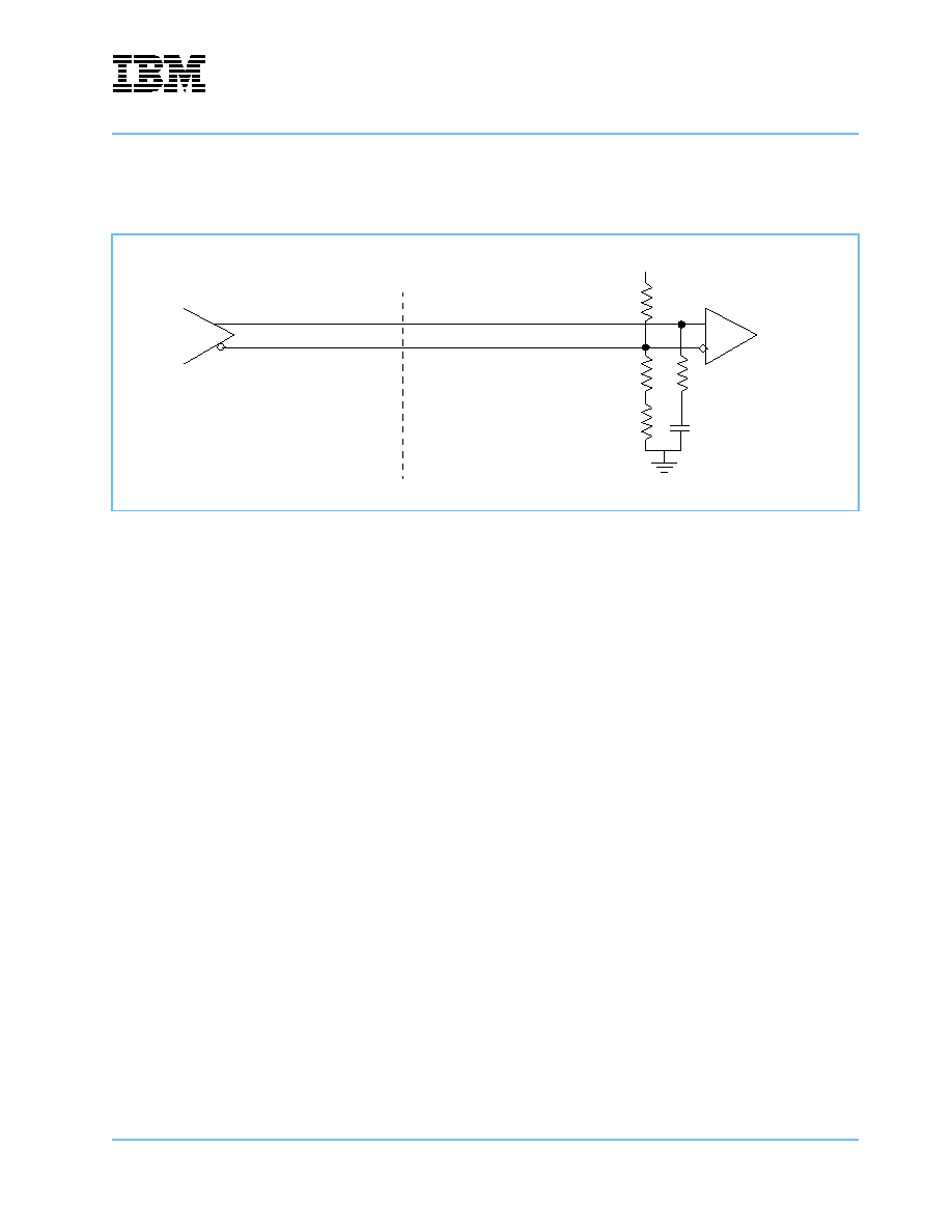
PRS28.4G
IBM Packet Routing Switch
prs28.04.fm
February 6, 2001
Line Termination
Page 129 of 131
Note: for the SYS_CLK_Q/QN differential pair, both termination resistors can be directly connected to GND,
without the use of the capacitor.
Figure 17: DASL Termination for Master LUs, Bits 2 and 3
DVR
51
�
5%
51
�
5%
10 nF
GND
V
DD
1.5K
�
5%
1
00 �
5%
Board Boundary

PRS28.4G
IBM Packet Routing Switch
Internal RAM ABIST
Page 130 of 131
prs28.04.fm
February 6, 2001
12. Internal RAM ABIST
The Array Built In Self Test (ABIST) is directly controllable from the OCM interface. When running ABIST, all
internal RAMs are tested. The test completes when all RAMs have been tested. Furthermore, the ABIST
Pass/Fail is a logical OR of the Fail Pass/Fail status of all individual RAM tests. In order to run ABIST, the
following sequence must be performed:
1. Perform chip reset (Power-On-Reset or Soft-Reset)
2. Issue the ABIST Start Command via the Command Register
3. Perform OCM Status Register Read commands. Bit 14 of the Status register is set to `1'b as long as the
ABIST is running. A `0'b at that position indicated the ABIST completed
4. Read the Miscellaneous Status Register. Bit 0 of that register indicates if the ABIST passed (`0'b) or failed
(`1'b).
The ABIST takes 1ms to complete.

PRS28.4G
IBM Packet Routing Switch
prs28.04.fm
February 6, 2001
References
Page 131 of 131
13. References
1. IEEE 1491.1 Specification "IEEE Standard Test Access Port and Boundary Scan Architecture"
2. CMOS5S6 Semi-Custom User's Guide. IBM Document Number PL-SC-C56, October 30, 1998
3. EIA/JEDEC Standard High Speed Transceiver Logic (HSTL) A 1.5V output Buffer Supply Voltage Based
Interface Standard for Digital Integrated Circuits EIA/JESD8-6 August 1995
Revision Log
Revision Date
Contents of Modification
August 25, 1999
Initial release (revision 00).
June 23, 2000
First revision (01). Added numbering to headings, tables, and figures.
July 10, 2000
Second revision (02). Added new Table of Contents, List of Figures, and List of Tables.
August 31, 2000
Third release (03).
Changed document title from IBM 28.4G Packet Routing Switch to IBM Packet Routing Switch PRS28.4G.
Changed reference to document type from Databook to Datasheet.
Changed page header labels from IBM 28.4G Packet Routing Switch to IBM Packet Routing Switch and from
IBM3209K4060 to PRS28.4G.
Changed references to IBM 28.4G Packet Routing Switch to IBM Packet Routing Switch PRS28.4G or
PRS28.4G as appropriate.
February 6, 2001
Fourth release (04).
Changed product number from IBM3209K4060 to IBM3221L0572.