ETIC
RESERVES THE RIGHT TO MAKE CHANGES AT ANY TIME TO IMPROVE THE DESIGN AND TO SUPPLY THE BEST PRODUCT.
© 2000, Rev A1
iC-Haus GmbH
Tel +49-6135-9292-0
Integrated Circuits
Fax +49-6135-9292-192
Am Kuemmerling 18, D-55294 Bodenheim
http://www.ichaus.com
Page 1 of 2
FEATURES
∑
Supply Voltage Range 4.5V to 30V
∑
Designed for phototransistor inputs
∑
Ungated index channel
∑
Current sink for LED drive (see application note
APP-D2)
∑
Outputs short circuit protected
∑
25mA peak drive current
3 CHANNEL DIFFERENTIAL
AMPLIFIER-COMPARATOR
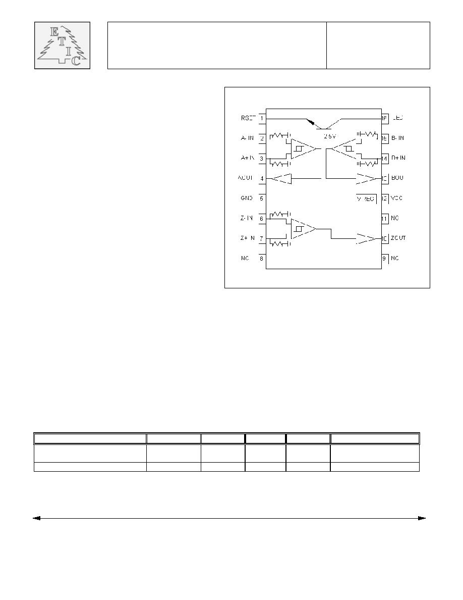
Phototransistor input version of the standard ET9560
ET9561
DESCRIPTION
These devices are specifically designed as receiver circuits for the phototransistor signals available in some optical
encoders. Connect the emitters of the phototransistors to the input pins, with the collectors connected to Vcc. The
inputs have 330 ohm resistors to terminate the phototransistors in an emitter follower mode. Differential inputs
enhance noise rejection and performance over temperature. Care should be taken to use phototransistors on
differential input pairs which have similar values of DC leakage current, as large differences in this charactersitic will
affect waveform symmetry.
APPLICATIONS
∑
Optical Encoders
∑
Industrial Controls
ABSOLUTE MAXIMUM RATINGS
Parameter
Symbol
Min.
Max.
Units
Ref.
Operating Temperature
Range
T
A
-40
125
∞C
Note 1
Supply Voltage Range
V
CC
4.5
30
V
ETIC
RESERVES THE RIGHT TO MAKE CHANGES AT ANY TIME TO IMPROVE THE DESIGN AND TO SUPPLY THE BEST PRODUCT.
© 2000, Rev A1
iC-Haus GmbH
Tel +49-6135-9292-0
Integrated Circuits
Fax +49-6135-9292-192
Am Kuemmerling 18, D-55294 Bodenheim
http://www.ichaus.com
Page 2 of 2
ELECTRICAL CHARACTERISTICS
Unless otherwise specified, typical values given at V
CC
=12V, T
A
= 25∞C, with LED and RSET open.
Parameters
Symbol
Min.
Typ.
Max.
Units
Test Conditions
High Level Supply Current
I
CCH
1
I
CCH
2
4.0
4.5
6.7
7.5
11.0
12.0
mA
Vcc = 4.5 V
Vcc = 30.0V
Peak Photocurrent Input
I
IP
0.3
0.5
15
mA
Note 2
Dark Cell Level
I
ID
0.0
0.05
7.5
mA
Photocurrent Contrast Ratio
I
R
2:1
-
-
Peak:Dark Cell
Hysteresis at Comparator Inputs
I
H
6
11
20
mV
Output High Level Voltage
V
OH
2.5
28.0
3.0
28.5
V
I
OH
= -4mA,V
CC
= 4.5V
I
OH
= -4mA,V
CC
= 30V
Output Low Level Voltage
V
OL
199
400
mV
V
CC
= 4.5V-30V
I
OL
= 8mA
Output Short-Circuit Current
Driving High (All Outputs)
I
OS
15
25
50
mA
V
CC
= 5V, V
OUT
= 0V
Output Short-Circuit Current
Driving Low (All Outputs)
I
OS
30
70
120
mA
V
CC
= 5V, V
OUT
= 5V
RSET Voltage
V
RSET
1.3
1.7
2.1
V
R = 180 ohms
AC SWITCHING CHARACTERISTICS
Values given at V
CC
= 5V, T
A
= 25∞C,
C
L
= 15pF on all outputs.
Parameters
Symbol
Min.
Typ.
Max
.
Units
Test Conditions
Propagation delay from Comparator
Input to Output
T
PD
850
ns
Output Rise Time
T
R
100
ns
Output Fall Time
T
F
20
ns
NOTES:
1. This is not a test parameter, but for information
only.
2. Higher signal levels can be handled by adding
resistors from the inputs to ground.
PACKAGE
SUFFIX
Chip Only
-C
16 Lead SOIC
-SOP