iC-JRX
µP INTERFACE WITH 2◊4 24V HIGH-SIDE DRIVERS
Rev A1, Page 1/23
PLCC44
VB -5.8V
-
IO0
IN
IL0
IL1
IL1
IL0
D
D
Q
VT
&
&
&
Toff1
Toff2
3.8V
+
D3
D4
D5
D6
D7
A0
A1
A2
A3
A4
D0
D1
D2
E/A LOGIK
iC-JRX
E/A LOGIK
E/A LOGIK
E/A LOGIK
E/A LOGIK
E/A LOGIK
E/A LOGIK
E/A LOGIK
Q
RESN
GNDD
RDN
WRN
CSN
VCCD
VCCA
NIOL
IO0
SC0
PSEL0
PEN0
OUT0
INTN
BLFQ
CLK
TEST
POE
GNDA
PGND
IO7
IO6
IO5
VB67
IO4
VB45
IO3
IO2
IO1
VB23
IO0
VB01
EIN-/AUSGANG STUFE 0
EIN-/AUSGANG STUFE 1
EIN-/AUSGANG STUFE 2
EIN-/AUSGANG STUFE 3
EIN-/AUSGANG STUFE 4
EIN-/AUSGANG STUFE 5
EIN-/AUSGANG STUFE 6
EIN-/AUSGANG STUFE 7
NIOL
PSEL0
SC0
OUT
POE
NTC
0µA
200µA
0µA
200µA
600µA
2.0mA
IH1
IH0
NIOH
30
34
1
2
3
39
40
41
42
43
38
8
37
9
36
10
35
11
12
7
6
4
5
15
31
16
23
17
19
18
20
22
21
24
26
25
27
29
28
UNTERSPANNUNGS-
ERKENNUNG VCCA
FEATURES
APPLICATIONS
À
2 ◊ 4 bidirectional input/output stages at 24 V
À
Input/output mode programmable in 4-bit blocks
À
Guaranteed high-side driving capability of 100 mA
dc
and
500 mA
peak
for pulse load
À
Short-circuit-proof drivers with high dielectric strength
À
Low saturation voltage of 0.6 V at 100 mA and 2 V at 500 mA
À
Integrated flyback circuits
À
PWM function with programmable duty cycle
À
Flash mode for the outputs
À
Power outputs can be disabled together
À
Programmable current sources define logic levels and allow
load monitoring
À
Digital input filters with externally adjustable filtering times
À
Can be bus operated due to the high-speed µP interface
À
Programmable interrupt output
À
Voltage and two-stage temperature monitoring
À
Dual quad high-side driver as a
bidirectional µP interface with
digital filtering in industrial 24 V
applications
PACKAGES
BLOCK DIAGRAM
Copyright © 2003, iC-Haus
www.ichaus.com
iC-JRX
µP INTERFACE WITH 2◊4 24V HIGH-SIDE DRIVERS
Rev A1, Page 2/23
LA2
LA3
REL1
S2
S1
µP
S4
S3
LA1
D0..D7
A0..A7
ADRESS-
DEKODIERER
RESET
CONTROLLER
8
5
8
RD
RES
INT
WR
VB45
21
18
VB67
VCCA
30
34
VCCD
WRN
2
IO4
20
IO5
IO6
19
IO7
17
PGND
23
3
RDN
7
RESN
28
VB01
VB23
25
16
GNDA
GNDD
12
INTN
6
IO0
29
IO1
27
26
IO2
IO3
24
22
1
D0
38
8
D1
D2
36
9
D3
D4
36
10
D5
35
D6
11
D7
39
A0
40
A1
A2
41
A3
42
43
A4
4
BLFQ
5
CLK
CSN
5 V
5 V
5 V
5 V
24 V
5 V
24 V
HIGHER
NIBBLE
NIBBLE
KONTROLL-
REGISTER
LOWER
PLCC44
iC-JRX
1.25 MHz
C1
100 nF
TEST
15
POE
31
C3 100 nF
C4 100 nF
C5 100 nF
C6 100 nF
C2
3.3 ... 10 uF
DESCRIPTION
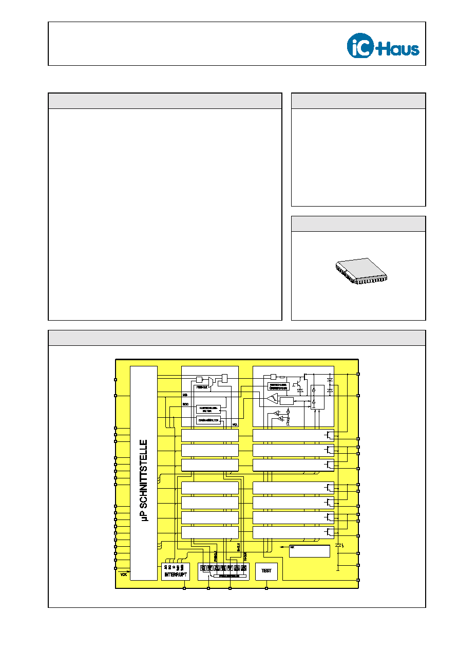
iC-JRX is an 8-fold high-side driver with integrated control logic, internally divided into two independent blocks
(nibbles). Both blocks can be individually set to input or output. The µP interface is made up of eight data, five
address and three control pins. Two further clock inputs control internal sequences (input filter, pulse
operation of the outputs). Starting with reset state, various register partitionings dependent on the selected
operating mode are possible.
Input mode is used to log logic levels at 24 V. An interrupt message can be generated when a signal at the
inputs changes. Spurious signals are rejected by the device's adjustable digital filters. When the inputs are
open the programmable pull-down current sets defined levels and acts as the bias current for switching
contacts.
In output mode the power output stages can drive any desired load to GND (e.g. lamps, long cables or relays)
at a continuous current of 100 mA or 500 mA in pulse operation. Spikes and flyback currents are discharged
through the integrated flyback circuits. All output stages are short-circuit-proof and two-stage temperature
monitoring (with interrupt messages) protects against thermal damage caused by large power dissipation. A
short circuit at one of the outputs can cause an interrupt; the current short circuit status can be scanned via
the µP interface. Pulse mode can be selected for each output, such as for indicator lamps in plugboards, in
order to offload the control software used. The actual switching level of the output can be read out via the µP
interface and be used to check for cable fractures with the pull-up currents. A PWM signal can also be
switched to any selected output. All outputs can be switched off via a mutual disable input e.g. by a processor-
independent watchdog circuit.
An interrupt pipeline which prevents the loss of interrupts allows reliable processing of interrupts using the
applied control software.
With low voltage the voltage monitor resets all registers and in doing so switches off the power output stages.
Diodes protect all inputs and outputs against ESD. The device is also immune to burst transients according
to IEC 1000-4-4 (4 kV; previously IEC 801-4).
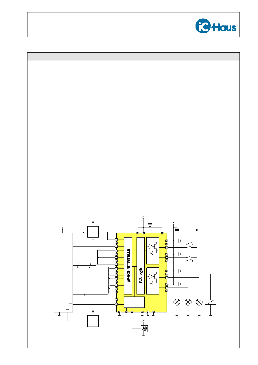
Typical application circuit
iC-JRX
µP INTERFACE WITH 2◊4 24V HIGH-SIDE DRIVERS
Rev A1, Page 3/23
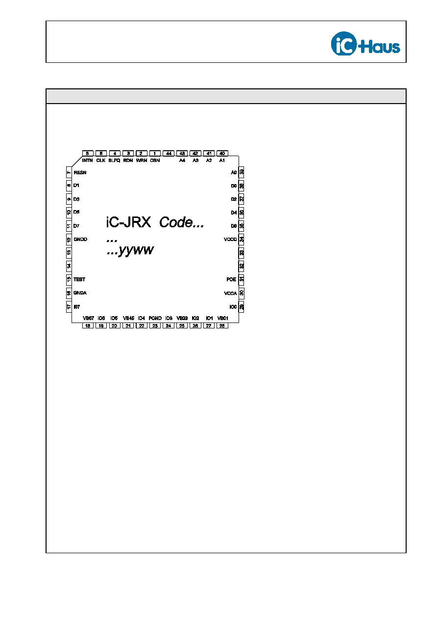
PACKAGES PLCC44 to JEDEC Standard
PIN CONFIGURATION PLCC44
(top view)
PIN FUNCTIONS PLCC44
No. Name
Fct.
Description No. Name
Fct.
Description
1
CSN
I
Chip Select, active low
23
PGND
Ground (ESD protection circuitry)
2
WRN
I
Write Enable, active low
24
IO3
B
I/O Stage 3
3
RDN
I
Read Enable, active low
25
VB23
Power Supply Driver Stage 2+3
4
BLFQ
I
Clock Flash Mode
26
IO2
B
I/O Stage 2
5
CLK
I
Clock Filter and PWM Function
27
IO1
B
I/O Stage 1
6
INTN
O
Interrupt Message, active low
28
VB01
Power Supply Driver Stage 0+1
7
RESN
I
Reset, active low
29
IO0
B
I/O Stage 0
8
D1
B
Data Bus Bit 1
30
VCCA
+5 V Supply Voltage (analog section)
9
D3
B
Data Bus Bit 3
31
POE
I
Power Output Enable
10
D5
B
Data Bus Bit 5
32
n.c.
11
D7
B
Data Bus Bit 7
33
n.c.
12
GNDD
Ground (digital section)
34
VCCD
+5 V Supply Voltage (digital section)
13
n.c.
35
D6
B
Data Bus Bit 6
14
n.c.
36
D4
B
Data Bus Bit 4
15
TEST
B
Test Pin
37
D2
B
Data Bus Bit 2
16
GNDA
Ground (analog section)
38
D0
B
Data Bus Bit 0
17
IO7
B
I/O Stage 7
39
A0
I
Address Bus Bit 0
18
VB67
Power Supply Driver Stage 6+7
40
A1
I
Address Bus Bit 1
19
IO6
B
I/O Stage 6
41
A2
I
Address Bus Bit 2
20
IO5
B
I/O Stage 5
42
A3
I
Address Bus Bit 3
21
VB45
Power Supply Driver Stage 4+5
43
A4
I
Address Bus Bit 4
22
IO4
B
I/O Stage 4
44
n.c.
Functions: I = Input, O = Output, B = bidirectional
External wiring VCCA, VCCD to +5 V and GNDA, GNDD, PGND to 0 V required.
iC-JRX
µP INTERFACE WITH 2◊4 24V HIGH-SIDE DRIVERS
Rev A1, Page 4/23
PROGRAMMING
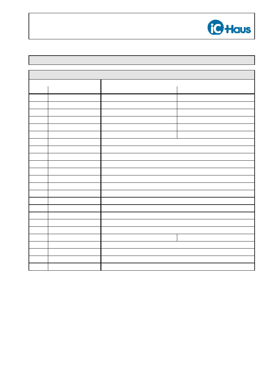
Register Overview
Address
A(4..0)d A4 A3 A2 A1 A0 Write
Read
0
0
0
0
0
0
-
Input Register
1
1
0
0
0
0
1
-
Change-of-input Message
2
2
0
0
0
1
0
-
Interrupt Status Register
3
0
0
0
1
1
-
Overcurrent Message
3
4
0
0
1
0
0
-
Overcurrent Status
5
0
0
1
0
1
-
Device ID
6
0
0
1
1
0
Output Register
7
0
0
1
1
1
Flash Pulse Enable
8
0
1
0
0
0
Change-of-input Interrupt Enable
4
9
0
1
0
0
1
Overcurrent Interrupt Enable
10
0
1
0
1
0
Control Word 1 (I/O filters)
11
0
1
0
1
1
Control Word 2 (I/O pin functions)
12
0
1
1
0
0
Control Word 3 (flash pulse settings)
13
0
1
1
0
1
Control World 4 (filter settings for overcurrent message)
14
0
1
1
1
0
Control Word 5 (PWM enable and pin selection)
15
0
1
1
1
1
PWM Register
16
1
0
0
0
0
-
...
...
...
...
...
...
-
26
1
1
0
1
0
-
27
1
1
0
1
1
-
A/D Interface
28
1
1
1
0
0
Test Register 1
29
1
1
1
0
1
Test Register 2
30
1
1
1
1
0
Test Register 3
31
1
1
1
1
1
Test Control Register
1
) Reads the inputs or reads back the outputs, depending on I/O pin mode
2
) For I/O pins in input mode (register is `0' in output mode)
3
) For I/O pins in output mode (register is `0' in input mode)
4
) Only writable in input mode
iC-JRX
µP INTERFACE WITH 2◊4 24V HIGH-SIDE DRIVERS
Rev A1, Page 5/23
Control Word 1 (I/O filters)
Add.: 10
reset entry: 00h
higher nibble
lower nibble
Bit
Name
7
BYPH
6
-
5
FH1
4
FH0
3
BYPL
2
-
1
FL1
0
FL0
higher nibble
Bit 7
BYPH
0
1
I/O filters active
(r)
Bypass for I/O filters: the I/O signals are reprocessed in their unfiltered state.
Bit 5..4
FH1..0
FH1
FH0
Filter times
0
0
1
1
0
1
0
1
14.5 ◊ tc(CLK)
± 1 ◊ tc(CLK)
896.5 ◊ tc(CLK)
± 64 ◊ tc(CLK)
3584.5 ◊ tc(CLK)
± 256 ◊ tc(CLK)
7168.5 ◊ tc(CLK)
± 512 ◊ tc(CLK)
lower nibble
Bit 3
BYPL
0
1
I/O filters active
(r)
Bypass for I/O filters: the I/O signals are reprocessed in their unfiltered state.
Bit 1..0
FL1..0
FL1
FL0
Filter times
0
0
1
1
0
1
0
1
14.5 ◊ tc(CLK)
± 1 ◊ tc(CLK)
(r)
896.5 ◊ tc(CLK)
± 64 ◊ tc(CLK)
3584.5 ◊ tc(CLK)
± 256 ◊ tc(CLK)
7168.5 ◊ tc(CLK)
± 512 ◊ tc(CLK)
'-'
Free memory location without a function. Status after a reset is `0'
'xx'h Indicates hexadecimal data for logic states. `x' indicates binary data
(r)
Status after a reset