 | –≠–ª–µ–∫—Ç—Ä–æ–Ω–Ω—ã–π –∫–æ–º–ø–æ–Ω–µ–Ω—Ç: iC-NQ | –°–∫–∞—á–∞—Ç—å:  PDF PDF  ZIP ZIP |

iC-NQ
13-Bit Sin/D CONVERTER WITH CALIBRATION
Rev A3, Page 1/15
TSSOP20
FEATURES
APPLICATIONS
À
Resolution of up to 8192 angle steps per sine/cosine period
À
Binary and decimal resolution settings, e.g. 500, 512, 1000,
1024; programmable angle hysteresis
À
Conversion time of just 250ns including amplifier settling
À
Count-safe vector follower principle, realtime system with
50MHz sampling rate
À
Direct sensor connection; selectable input gain
À
Front-end signal conditioning features offset (8 bit),
amplitude ratio (5 bit) and phase (6 bit) calibration
À
250kHz input frequency
À
Parameterization and absolute angle output via bidirectional
high-speed synchronous-serial BiSS interface
À
A QUAD B incremental outputs with selectable minimum
transition distance (e.g. 0.125µs for 2MHz at A)
À
Index signal processing adjustable in position and width
À
Fault monitoring: frequency, amplitude, configuration (CRC)
À
Fast 24-bit on-chip multiturn counter
À
Fully re-programmable by BiSS interface with access to
serial EEPROM to store setup and customer data
À
ESD protection and TTL-/CMOS-compatible outputs
À
Interpolator IC for position data
acquisition from analog
sine/cosine sensors
À
Optical linear/rotary encoders
À
MR sensor systems
PACKAGES
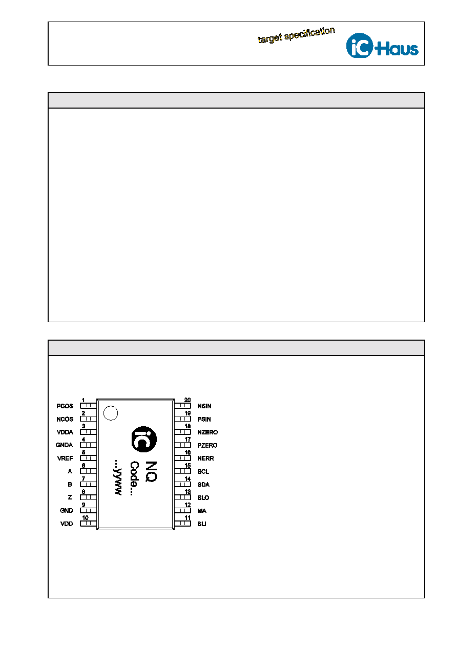
BLOCK DIAGRAM
© 2003
iC-Haus GmbH
Tel. +49-6135-9292-0
Integrated Circuits
Fax +49-6135-9292-192
Am Kuemmerling 18, D-55294 Bodenheim
http://www.ichaus.com
-
+
-
+
INPUT SIN
Sin/D CONVERSION
E2PROM
INTERFACE
BiSS
INTERFACE
INCREMENTAL
OUTPUT
CORRECTION
CONTROL LOGIC
ARCTAN
COS
-
+
-
+
SIN
VDDA
VREF
+
-
INPUT ZERO
RAM
COUNTER
24-BIT COUNTER
iC-NQ
INPUT COS
Z
SLO
VDD
VDDA
VREF
PCOS
PSIN
PZERO
SCL
SDA
SLI
MA
NCOS
NERR
NSIN
NZERO
A
B
GND
GNDA
PHASE
iC-NQ
13-Bit Sin/D CONVERTER WITH CALIBRATION
Rev A3, Page 2/15
DESCRIPTION
iC-NQ is a monolithic A/D converter which, by applying a count-safe vector follower principle, converts
sine/cosine sensor signals with a selectable resolution and hysteresis into angle position data. This absolute
value is output via a high-speed synchronous-serial BiSS interface and trails a master clock rate of up to 10
Mbit/s, or, alternatively, can be set so that it is compatible with SSI. A 24-bit period counter which can be read
using BiSS multicycle data (MCD) supplements the position data with a multiturn count.
At the same time any changes in output data are converted into incremental A QUAD B encoder signals.
Here, the minimum transition distance can be adapted to suit the system on hand (cable length, external
counter). A synchronized zero index is generated and output to Z if enabled by the PZERO/NZERO inputs.
The front-end amplifiers are configured as instrumentation amplifiers, permitting sensor bridges to be directly
connected without the need for external resistors. Various programmable D/A converters are available for the
conditioning of sine/cosine sensor signals with regard to offset, amplitude ratio and phase errors. Front-end
gain can be set in stages graded to suit all common differential sensor signals from approximately 20mVpp
to 1.5Vpp, and also single-ended sensor signals from 40mVpp to 3Vpp respectively.
Two serial interfaces have been included to permit configuration of the device, connection of an EEPROM or
synchronous-serial data transfer (BiSS). Both interfaces are bidirectional and enable the complete
configuration of the device including the transfer of setup and system data to the EEPROM for permanent
storage.
If the memory is detected following a power-down reset, the chip setup is read in and automatically repeated
if a CRC error occurs.
PACKAGE TSSOP20 to JEDEC Standard
PIN CONFIGURATION TSSOP20 4.4mm
PIN FUNCTIONS
(top view)
No. Name Function
1
PCOS
Input Cosine %
2
NCOS
Input Cosine &
3
VDDA
+5V Supply Voltage (analog)
4
GNDA
Ground (analog)
5
VREF
Reference Voltage
6
A
Incremental Output A
7
B
Incremental Output B
8
Z
Output Index Z
9
GND
Ground
10 VDD
+5V Supply Voltage (digital)
11 SLI
BiSS interface, data input
12 MA
BiSS interface, clock line
13 SLO
BiSS interface, data output
14 SDA
EEPROM interface, data line
15 SCL
EEPROM interface, clock line
16 NERR
Error output, active low
17 PZERO Input Zero Signal %
18 NZERO Input Zero Signal &
19 PSIN Input
Sine
%
20 NSIN
Input Sine &
External connections linking VDDA to VDD and
GND to GNDA are required.
iC-NQ
13-Bit Sin/D CONVERTER WITH CALIBRATION
Rev A3, Page 3/15
All voltages are referenced to ground unless otherwise noted.
All currents into the device pins are positive; all currents out of the device pins are negative.
ABSOLUTE MAXIMUM RATINGS
Values beyond which damage may occur; device operation is not guaranteed.
Item Symbol
Parameter
Conditions
Fig.
Unit
Min.
Max.
G001 VDDA
Analog Supply Voltage
-0.3
6
V
G002 VDD
Digital Supply Voltage
-0.3
6
V
G003 V()
Voltage at
PSIN, NSIN, PCOS, NCOS, PZERO,
NZERO, VREF, NERR, SCL,
SDA, MA, SLI, SLO, A, B, Z
V() < VDDA+0.3V
V() < VDD+0.3V
-0.3
6
V
G004 Imx(VDDA) Current in VDDA
-50
50
mA
G005 Imx(GNDA) Current in GNDA
-50
50
mA
G006 Imx(VDD)
Current in VDD
-50
50
mA
G007 Imx(GND) Current in GND
-50
50
mA
G008 Imx()
Current in
PSIN, NSIN, PCOS, NCOS, PZERO,
NZERO, VREF, NERR, SCL,
SDA, MA, SLI, SLO, A, B, Z
-10
10
mA
G009 Ilu()
Pulse Current in all pins
(Latch-up Strength)
pulse duration < 10ms
-100
100
mA
EG1 Vd()
ESD Susceptibility
at all pins
MIL-STD-883, Method 3015, HBM
100pF discharged through 1.5k
2
kV
TG1 Tj
Operating Junction Temperature
-40
150
∞C
TG2 Tj
Storage Temperature Range
-40
150
∞C
THERMAL DATA
Operating Conditions: VDDA= VDD= 5V ±10%
Item Symbol
Parameter
Conditions
Fig.
Unit
Min.
Typ.
Max.
T1
Ta
Operating Ambient Temperature Range
(extended range on request)
-20
85
∞C

iC-NQ
13-Bit Sin/D CONVERTER WITH CALIBRATION
Rev A3, Page 4/15
ELECTRICAL CHARACTERISTICS
Operating Conditions: VDDA= VDD= 5V ±10%, Tj= -40..125∞C, unless otherwise noted
Item
Symbol
Parameter
Conditions
Tj
Fig.
Unit
∞C
Min.
Typ.
Max.
Total Device
001 VDDA,
VDD
Permissible Supply Voltage
4.5
5.5
V
002 I(VDDA) Supply Current in VDDA
fin()= 200kHz; A, B, Z open
15
mA
003 I(VDD)
Supply Current in VDD
fin()= 200kHz; A, B, Z open
5
mA
004 Von
Turn-on Threshold VDDA, VDD
-40
27
85
125
2.2
2.0
3.7
3.3
2.8
2.7
4.4
V
V
V
V
005 Vc()hi
Clamp Voltage hi at
PSIN, NSIN, PCOS, NCOS,
PZERO, NZERO, VREF
Vc()hi= V() -VDDA;
I()= 1mA, other pins open
0.3
1.6
V
006 Vc()lo
Clamp Voltage lo at
PSIN, NSIN, PCOS, NCOS,
PZERO, NZERO, VREF, NERR,
SCL, SDA, MA, SLI, SLO, A, B, Z
I()= -1mA, other pins open
-1.5
-0.3
V
007 Vc()hi
Clamp Voltage hi at
NERR, SCL, SDA, MA,
SLI, SLO, A, B, Z
Vc()hi= V()-VDD;
I()= 1mA, other pins open
0.3
1.6
V
Input Amplifiers PSIN, NSIN, PCOS, NCOS
101 Vos()
Input Offset Voltage
Vin() and G() in accordance with
Gain Select table; G
$20
G <20
-10
-15
10
15
mV
mV
102 TCos
Input Offset Voltage
Temperature Drift
see 101
mV/K
103 Iin()
Input Current
V()= 0V.. VDDA
-50
50
nA
104 GA
Gain Accuracy
G() in accord. with Gain Sel. table
95
102
%
105 GArel
Gain SIN/COS Ratio Accuracy
G() in accord. with Gain Sel. table
97
103
%
106 fhc
Cut-off Frequency
G= 80
G= 2.667
250
700
kHz
kHz
107 SR
Slew Rate
G= 80
G= 2.667
4.5
10
V/µs
V/µs
Sin/D Conversion: Accuracy
201 AAabs
Absolute Angle Accuracy
referred to 360∞ input signal,
G= 2.667, Vin= 1.5Vpp
-1.0
1.0
DEG
202 AArel
Relative Angle Accuracy
referred to period of A output sig-
nal, G= 2.667, Vin= 1.5Vpp,
SELRES= 1024
-10
10
%
Reference Voltage VREF
801 VREF
Reference Voltage
I(VREF)= -1mA..+1mA
48
52
%
VDDA
Oscillator
A01 f(OSC)
Oscillator Frequency
presented at SCL with subdivision
of 2048;
VDDA= VDD= 5V ±10%
VDDA= VDD= 5V
27
52
62
69
82
76
MHz
MHz
A02 TC(OSC) Oscillator Frequency
Temperature Drift
VDDA= VDD= 5V
-0.1
%/K
A03 VC(OSC) Oscillator Frequency Power
Supply Dependance
+10.6
%/V

iC-NQ
13-Bit Sin/D CONVERTER WITH CALIBRATION
Rev A3, Page 5/15
ELECTRICAL CHARACTERISTICS
Operating Conditions: VDDA= VDD= 5V ±10%, Tj= -40..125∞C, unless otherwise noted
Item
Symbol
Parameter
Conditions
Tj
Fig.
Unit
∞C
Min.
Typ.
Max.
Zero Comparator
E01 Vos()
Input Offset Voltage
V()= Vcm()
-20
20
mV
E02 Iin()
Input Current
V()= 0V.. VDDA
-50
50
nA
E03 Vcm()
Common-Mode Input Voltage
Range
1.4
VDDA-
1.5
V
E04 Vdm()
Differential Input Voltage Range
0
VDDA
V
Incremental Interface, BiSS Interface: Outputs A, B, Z, SLO
D01 Vs()hi
Saturation Voltage hi
Vs()hi= VDD-V(); I()= -4mA
0.4
V
D02 Vs()lo
Saturation Voltage lo
I()= 4mA
0.4
V
D03 tr()
Rise Time
CL()= 50pF
60
ns
D04 tf()
Fall Time
CL()= 50pF
60
ns
BiSS Interface: Inputs MA, SLI
D05 Vt()hi
Threshold Voltage hi
2
V
D06 Vt()lo
Threshold Voltage lo
0.8
V
D07 Vt()hys
Hysteresis
Vt()hys= Vt()hi-Vt()lo
300
mV
D08 Ipu(MA)
Pull-up Current in MA
V()= 0..VDD-1V
-240
-120
-25
µA
D09 Ipd(SLI)
Pull-down Current in SLI
V()= 1..VDD
20
120
300
µA
D10 CLK(MA) Permis. Clock Frequency at MA
sensor mode
register mode
10
250
MHz
kHz
EEPROM Interface, Control Logic: Inputs SDA, NERR
D11 Vt()hi
Threshold Voltage hi
2
V
D12 Vt()lo
Threshold Voltage lo
0.8
V
D13 Vt()hys
Hysteresis
Vt()hys= Vt()hi-Vt()lo
300
mV
EEPROM Interface, Control Logic: Outputs SDA, SCL, NERR
D14 Vs()lo
Saturation Voltage lo
I()= 4mA
0.4
V
D15 Ipu()
Pull-up Current
V()= 0..VDD-1V
-600
-300
-75
µA
D16 tf()
Fall Time
CL()= 50pF
60
ns
D17 tmin()lo
Error Signal Minimal Duration
at NERR
10
ms
D18 Tpwm()
Error Signal PWM Cycle Duration
at NERR
f(OSC) subdivided by 2
22
61.7
ms